Strong pinning in high temperature superconducting films
Abstract
Detailed measurements of the critical current density of YBa2Cu3O7-δ films grown by pulsed laser deposition reveal the increase of as function of the film thickness. Both this thickness dependence and the field dependence of the critical current are consistently described using a generalization of the theory of strong pinning of Ovchinnikov and Ivlev [Phys. Rev. B 43, 8024 (1991)]. From the model, we deduce values of the defect density () and the elementary pinning force, which are in good agreement with the generally accepted values for Y2O3–inclusions. In the absence of clear evidence that the critical current is determined by linear defects or modulations of the film thickness, our model provides an alternative explanation for the rather universal field dependence of the critical current density found in YBa2Cu3O7-δ films deposited by different methods.
pacs:
74.60.Ec,74.40.Jg,74.60.GeI Introduction
High vortex pinning forces leading to high critical currents are an indispensable prerequisite for superconducting thin films if these are to be used in electronic and power applications. The “volume” pinning force exerted by material impurities on flux vortices opposes their motion, which is at the origin of flux noise and dissipation. Strong vortex pinning decreases noise in electronic and superconducting quantum interference devices (SQUID’s) and leads to high quality factors necessary for the correct operation of radio-frequency and microwave filters and cavities. Present-day films of the high temperature superconductor YBa2Cu3O7-δ combine high critical current density [1] with a high critical temperature and are thus ideal candidates for widespread application. The optimization of the critical current through identification and tailoring of defect microstructures which lead to high pinning and reduced vortex creep has therefore attracted a lot of interest in the High Temperature Superconductor (HTC) community.
Several types of pinning defects have been suggested as being responsible for the large ’s in HTC films. Foremost are the oxygen vacancies in the strongly superconducting CuO2 layers of these materials. Due to the small coherence length and the large condensation energy of the cuprates, such vacancies are potentially very effective pinning centers; their effect may in principle explain the high critical currents encountered in YBa2Cu3O7-δ films.[2, 3] Vortex pinning by these dense defects of typical diameter is best described by the theory of weak collective flux pinning,[2, 4, 5] in which a net force on the vortex lattice exists only as a result of fluctuations in the defect density ( is the effective defect density and is the anisotropy parameter of the superconductor, for YBa2Cu3O7). The volume pinning force is obtained from , where the pinning strength , is the elementary force exerted by one defect on a vortex line, and the averaging is carried out over a unit cell of the vortex lattice. The correlated volume , where the correlation lengths and are the distances, respectively parallel and perpendicular to the magnetic induction, at which the relative displacements due to pinning and are equal to .
The very high measured values Am-2 (see below) imply, however, that does not, under usual experimental conditions, exceed the vortex spacing . [6] In other words, the small scale displacements of neighboring vortices are independent. An estimate of the longitudinal correlation length (or “Larkin length”) under the condition ,
| (1) |
shows that nm, much less than usual film thicknesses nm. Here is the depairing current density, is the typical vortex energy scale, is the flux quantum, is the penetration depth for supercurrents flowing in the CuO2–layers, and . Contrary to the case of weakly pinning films in the two–dimensional limit, in which ,[7] the critical current density
| (2) |
is field– and thickness–independent. Using the explicit form for oxygen vacancies, where is the oxygen ion radius, one has
| (3) |
Note, however, that underdoped twin-free YBa2Cu3O7-δ single crystals, in which the increase of the sustainable current density due to an increasing density of oxygen vacancies in the CuO2–layers as one underdopes the material is consistent with a concomitant decrease of ,[8] show an exponential temperature dependence of the current density that is not observed in thin films.
YBa2Cu3O7-δ films typically form through two-dimensional nucleation and island growth,[9, 10] with lateral island sizes that increase with growth temperature and film thickness.[11, 12] The significant thickness modulations related to the presence of the islands and the associated variations of the vortex line energy as function of the position, lead to pinning of vortices in the thinnest portions of the film. The maximum pinning force will be close to that needed to drive a single vortex line out of such a trough. If this mechanism is dominant, the experimentally measured critical current density is expected to follow
| (4) |
with the average island diameter.[2] In their detailed study of the relation between film roughness and the current density, Jooss et al. suggested that this is indeed the case.[13] However, the magnitude of the critical current density and its increase as function of the film thickness for films thinner than could only be explained by these authors by invoking the lowered vortex line tension in such thin films, in which the effective penetration depth is equal to , and by assuming an unidentified supplementary bulk pinning mechanism. Furthermore, the study[13] restricted itself to fields T and K.
The discovery of growth spirals with a central screw dislocation in sputtered or metal-organic chemical vapor deposited (MO-CVD) YBa2Cu3O7-δ films [9, 10] immediately lead to the suggestion that extended defects rather than microscopic point defects are the main pinning centers.[2] The growth spirals appear in laser-ablated films only when the substrate is heated above 850 ∘C during deposition in an oxygen pressure exceeding 50 Pa, while below this temperature, the films are formed through island growth.[12] In the latter case, screw– and edge dislocations are to be expected only in the troughs between islands, effectively halting easy vortex motion along these. Recent experiments by Dam et al. [14] showed that a “characteristic field” (or vortex density) beyond which the critical current density of YBa2Cu3O7-δ films decreases, is correlated with the surface density of screw dislocations . Sequential etching showed the screw dislocations to extend throughout the film thickness, allowing for the possibility that the vortices are pinned along their entire length on the non-superconducting dislocation core of radius .[14] The smallness of means that unlike amorphous columnar defects, to which the dislocation cores are often compared,[15] pinning is more likely to be due to the core-induced variation of the mean free path in the vicinity of the dislocation (–mechanism). Supposing that the pinning of an individual vortex line on a dislocation core leads to a critical current density , the critical current density at higher fields will be equal to times the fraction of pinned vortices . The latter is determined by the probability that a given vortex encounters at least one dislocation core in an allowed area determined by equating to the loss of elastic energy due to the deformation of the vortex lattice,[16, 17, 18] so that
| (5) | |||||
| (6) |
A similar formula was used by Dam et al. to deduce the value of the “characteristic field” . Due to the non-homogeneous current distribution in superconductors, depinning from the linear defects would be initiated by the nucleation at the film surface of vortex kinks joining two dislocation cores.[19] As a result, the experimentally measured low–field “critical” current should be rather smaller than the critical current density in the absence of flux creep and decay rapidly with time. The time decay will be even more rapid when the applied magnetic field and the vortices are not aligned along the dislocation cores. Hence, in analogy to the case of heavy-ion irradiation–induced amorphous tracks, pinning by extended linear screw dislocation cores should lead to a sharp cusp-like maximum in the field orientation–angle dependence of the experimentally measured critical current.[20, 21]
It should be remarked that both in the case of pinning by thickness variations and pinning by screw dislocations, the low–field critical current flows only at the film surface. Hence, the total screening current as well as the characteristic field of flux penetration in a magnetic experiment (see below) is independent of the film thickness , and the apparent current density decreases inversely proportional to .
In what follows, we present a detailed study of the critical current density of YBa2Cu3O7-δ films grown by pulsed laser deposition as function of film thickness, field magnitude and orientation, and temperature. It turns out that the field orientation– and thickness dependence of do not provide any evidence for pinning by screw dislocations or other correlated disorder in our films. Yet, the temperature and field dependence of is entirely comparable to that measured in films which contain these defects.[10, 14]
To explain our results, we propose that the relevant pinning centers in our films are sparse insulating or normal metallic second-phase inclusions. These are known to exist in sputter-deposited YBa2Cu3O7-δ films as platelet-like Y2O3 inclusions of size nm3, with typical densities .[22, 23] Other authors have reported the presence of Y2O3 inclusions in laser–ablated films as well, with typical densities m-3 for inclusions of diameter — 5 nm, and m-3 for 10 – 20 nm.[24, 25] Pinning by such large defects turns out to be conveniently described using an extension of the theory of strong pinning of Ovchinnikov and Ivlev [26], which we shall develop below (II). Our model is, to our knowledge, the only that consistently describes both the field- and thickness dependence of the critical current density in YBa2Cu3O7-δ films.
II Strong pinning by sparse large point pins
A General formulation
Strong pinning by large point defects has been described by simple substitution of the elementary pinning force of a large void into the collective pinning expression (2).[6] This procedure makes the implicit assumption that there are many inclusions in a region of volume . A comparison of the longitudinal correlation length, nm, which follows from a collective-pinning analysis of experimental critical current density–data, with the expected mean distance between large defects, nm, shows that this approach is inappropriate.
In order to obtain the critical current density for sparse pins, one should not start from the statistical average of the pinning forces of the different defects, but, rather, evaluate the probability that a vortex line will be pinned at all. A nearby defect will be able to trap a vortex line if the gain in pinning energy is sufficient to outweigh the elastic energy loss due to the vortex lattice deformation caused by displacing the vortex line onto the defect. The maximum allowed lateral displacement of the vortex determines the “trapping area” within which a large defect is an effective pinning site. The bulk (volume) pinning force is given by the direct sum of the elementary forces of the individual defects that can effectively pin a single vortex, i.e. those that lie within of the vortex lattice position, normalised by the volume available to the vortex. Any vortex line will be pinned on average by defects, where is the average distance between such “effective” pinning centers, so that
| (8) |
The probability to encounter a second effective defect at distance from a first defect located at is given by the product of the probability to encounter none in the interval and the probability to find at least one at . In the case of layered superconductors considered in Ref. [26], where the only effective defects are those situated in the CuO2 layers, this yields
| (9) | |||||
| (10) |
and . Here is the areal density of defects in the CuO2 layers and is the distance between layers. This result has the same “two–dimensional” form as the result ( LABEL:eq:SD-high-field ) for linear defects extending throughout the thickness of the film. For continuous[5] superconductors
| (11) |
which gives [26]
| (12) |
In the case of real samples (of finite thickness in the field direction), and especially for thin films, the derivation (11) becomes inappropriate in the limit , in which not every vortex line can find a defect. For such small defect densities or sample thicknesses, one should evaluate the probability that a vortex line encounters at least one defect in the volume . However, the same condition implies ; Hence, the critical current density has the same form as Eq. (12). We shall, therefore, assume that Eq. (12), valid for both and , is applicable irrespective of the defect density and the film thickness.[27]
B The trapping area
1 Pin Breaking
The trapping area and can be obtained using two different approaches, corresponding to the different mechanisms by which a vortex can be liberated from a defect: pin-breaking and plastic depinning.[28] The most obvious possibility is “pin-breaking”, in which the applied force must exceed the attractive force exerted by a defect on a vortex line. Plastic depinning only occurs if the pins can be considered as “infinitely strong”, i.e. , which is not the case in what follows. Exploiting the similarity of pinning by extended pointlike defects with pinning by amorphous columnar defects,[21] the elementary pinning force of an inclusion of extent (perpendicular to the field direction) can be estimated as the product of the fraction of the vortex core volume occupied by the defect and the condensation energy . Following Ref. [5], the resulting pinning force can be approximated by the interpolation
| (13) | |||||
| (14) |
where is the extent of the defect along the field direction. Note that the above expression corresponds to “–pinning”;[5] pinning by the variation of the mean-free path in the vicinity of the defect is relatively unimportant, because the quasiparticle scattering probability in the layer of thickness surrounding the defect is negligible as compared to the total scattering cross-section of the inclusion ( is the BCS coherence length).
The maximum allowed vortex displacement is obtained by balancing the elastic energy loss with the pinning energy gain . Taking explicitly into account the range of the pinning potential , Ovchinnikov and Ivlev obtained [26]
| (15) |
Here we have approximated the vortex lattice shear modulus and the nonlocal tilt modulus . Note that for fields in excess of the maximum allowed vortex excursion becomes comparable to , and .
| (16) | |||||
| (17) |
The above expression can be compared to the result of a simpler estimate, which follows from an approach initially suggested by Vinokur et al. to describe pinning by dense point pins and vortex wandering in layered superconductors.[29] The energy of elastic deformation of a representative vortex segment of length in its lattice cell is . Minimization with respect to yields the optimum length over which a vortex segment can fluctuate independently from its neighbors. Note that is equal to on condition that exactly. The distance , to which a vortex may wander, is obtained by equating the pinning energy gain to ; this gives
| (18) |
The critical current density
| (19) | |||||
| (20) |
with .
2 Low fields - single vortex limit
A glance at Eqs. (15)–(20) shows that at low fields the trapping area and hence the critical current have an unphysical divergence. The correct low–field limit of the trapping area is obtained by starting from the line tension of a single vortex line . Balancing the energy of elastic deformation of a single line with the pinning energy, , one has and
| (21) | |||||
| (22) |
The trapping area becomes and
| (23) | |||||
| (24) |
The single vortex limit is realized for fields such that , i.e. .
3 Very thin films
A second limit, in which the results of Section II B 1 do not hold is that of very thin films of thickness . Note that this condition is also violated at very low fields . In YBa2Cu3O7-δ we have ( mT) nm, which is comparable to typical film thicknesses. Under these conditions, the probability for a vortex to be trapped by an inclusion is determined by its ability to bend sufficiently within the film thickness, i.e. the tilt contribution dominates the elastic energy. We thus need to repeat our considerations for , which will minimize the elastic energy in this case. The total energy of a vortex in the cage of dimensions is given by
| (25) |
Equating this to zero yields , and the critical current density
| (26) |
Thus, for very thin films, the critical current density should be field-independent and increase linearly with film thickness.
Under the condition that , the crossover from the “thick thin film” single vortex limit [section (II B 2)] and the “thin thin film” limit occurs when the thickness is reduced below the crossover value
| (27) |
determined from the equation of the trapping areas in either limit.
III Experimental details
Thin films of YBa2Cu3O7-δ were deposited on 1.21.5 mm2 LaAlO3 substrates by KrF laser ablation from a stoichiometric target. The deposition was carried out onto substrates heated to 785∘ C at 280 mTorr (36.7 Pa) oxygen pressure, in the so-called “off-axis” geometry, i.e. the substrate surface was oriented parallel to the plasma plume axis. From previous experiments, we know this geometry to produce films featuring homogeneous flux penetration (on a m scale). We have prepared different series of films of seven different thicknesses, from 100 to 500 nm, using exactly the same deposition procedure. After deposition, the film edge was etched away to produce 0.90.9mm2 YBa2Cu3O7-δ squares used for further investigations.
The obtained films were characterized using X-ray diffraction with CrKα radiation and Atomic Force Microscopy (AFM). The diffraction experiments revealed
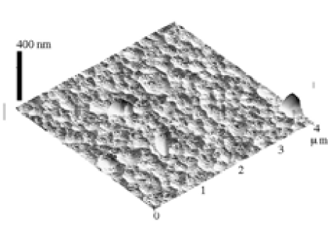
the existence (5 atomic % ) of a second (cubic) phase. In AFM experiments we observed a surface morphology characteristic of island growth, with occasional outgrowths (see Fig.1). The growth islands had a typical lateral size of about 300 nm. This is very similar to the results found by other authors under the same deposition conditions.[12, 14] We do not find the spiral growth mechanism to be relevant to our samples – a comparison with the deposition conditions of Ref. [12] indicates that growth spirals are not to be expected.
All films were characterized using the magneto-optical technique for flux visualization.[31] A ferrimagnetic garnet film with in-plane anisotropy is placed directly on top of the superconducting film. The garnet is observed using a polarized light microscope with nearly crossed polarizers. In this configuration, the reflected light intensity is proportional to the local magnetic induction perpendicular to the garnet, allowing the direct observation of flux penetration into the YBa2Cu3O7-δ film. The “critical” screening current density can be obtained directly from the distance between the flux front and the film edge at a given applied magnetic field and temperature, , where is half the film width and the “characteristic field” for flux penetration.[34] Alternatively, one can fit the position of the flux front as function of the applied field ,
| (28) |
to obtain the low-field limit of the current density . [13]
The magneto-optical imaging of the films was used not only to obtain current densities at fields smaller than 300 G, but also to select the most homogeneous films for magnetometry experiments using the Local Hall Probe Magnetometer.[32] A commercial miniature GaAs
Hall probe, placed in the center of the film surface, is used to measure the local induction as function of the applied magnetic field. The result is converted into the so-called “self–field” of the sample, , created by the circulating screening current. The latter was determined from the width of the hysteresis loop of at constant and calibrated using the values obtained from the magneto-optic experiments. In this way, the temperature– and field dependences of the screening current were measured in fields of up to 2 T and temperatures between 30 and 85 K. In order to obtain results in the temperature range close to , measurements in AC mode were carried out by applying a 1.5 Oe AC field of frequency 7.75 Hz. The AC Hall voltage , measured using a dual-reference lock-in amplifier, was converted to the in-phase fundamental transmittivity of the sample, .[33] Using this technique, the critical temperature of all films was found to be similar, ranging between 88.8 and 91.7 K.
IV Results
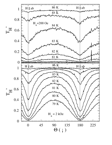
Transmittivity experiments as function of DC field orientation performed at different temperatures and field magnitudes do not reveal any cusp in the angular dependence of the transmittivity when is oriented along the film normal (Fig. 2). This indicates that it is unlikely that directional pinning by correlated disorder determines the critical current density. If such pinning is due to the dislocations cores, it is masked by another mechanism of strong pinning, which remains to be identified.
In order to evaluate the thickness dependence of the critical current density without ambiguities in the conversion of magnetic moment to current density, we turn
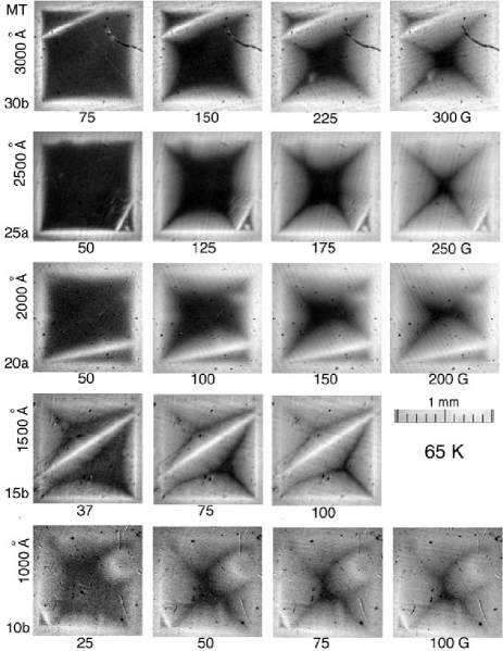
to magneto-optical imaging of the flux penetration. Fig. 3 shows the flux penetration into five films of thicknesses nm, at K. Nearly all films of this batch show at least one weak link, possibly due to the presence of a grain boundary in the substrate. These are easily rendered visible due to the preferential flux penetration along them. Nevertheless, the remaining areas feature homogeneous flux penetration and are sufficiently large to obtain reliable results for the flux front position and the screening current density. The image frames are chosen so that the vertical sequences have constant, a procedure that should yield similar flux penetration if the screening current would be the same for all films. It is clearly seen, however, that for constant flux penetration is easier in the thinner films. The effect is quantified by measuring the position of the flux-front relative to the film edge and converting
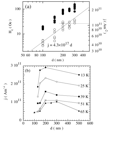
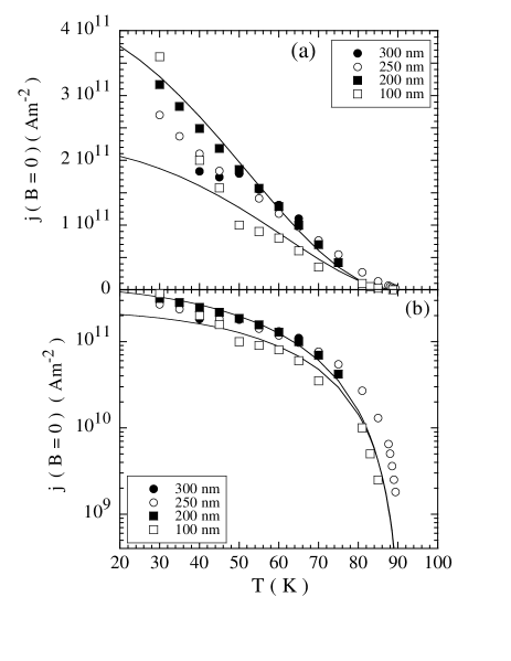
this to the characteristic field and screening current density using Eq. (28). The result of this procedure is plotted in Fig. 4(a). We find that manifestly increases before reaching a plateau for nm. This increase and the subsequent plateau is in contradiction both with the constant predicted for weak collective pinning (Eq. (2)), and with the constant and expected for pinning by linear defects or by thickness variations (Eq. (4)). However, it is in agreement with Eqs. (24) and (26) derived for sparse inclusions or large point pins, which predict that the sustainable current should increase with thickness before reaching a plateau for . The experimental data show a slope , which can be compared to the theoretical value predicted by Eq. (26). This yields, at 65 K, a defect density m-3, if we use Eq. (14) for the pinning force, nm and nm from TEM experiments, [22] Jm-1, nm, and K. The obtained defect density corresponds to a crossover thickness nm at 65 K, comparable to the experimental data.
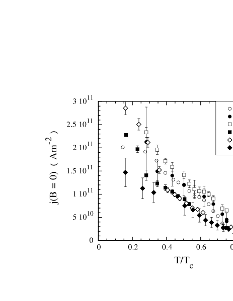
In order to check the plausibility of the above results, we have prepared two other series of YBa2Cu3O7-δ thin films using the same nominal deposition conditions. All films in these batches were homogeneous without grain boundaries. Magneto-optical measurements confirm the thickness dependence of the critical current density, as depicted in Figs. 4(b) and 5. For small film thicknesses, increases with , reaching a plateau for nm. The current density decreases again for the 500 nm–thick film, perhaps due to the deteriorating epitaxy as one increases the film thickness too much. The increase of the critical current density with the film thickness is observed at all temperatures. The only exception are the data for
the 150–nm thick films, for which tends to the values measured in thicker films at ( open diamonds in Fig. 5). A similar low–temperature behavior can be noted in Fig. 1 of Ref. [3]. This may either indicate that a background pinning by other types of defects such as dislocations or oxygen vacancies starts to play a role for K, or that the crossover thickness decreases with decreasing temperature, a behavior that may be expected from Eqs. (14) and (27).
The temperature dependence of the low–field critical current density can be rather well described using Eq. (26) and the same parameter values as above, as indicated by the lower continuous lines in Fig. 6 (a,b) (for nm). Fits using Eq. (24) for larger film thicknesses are equally successful [upper lines in Fig. 6(a,b)], although m-3 instead of m-3 should be used.
We now turn to the field dependence of the screening current. Typical results are depicted in Fig. 7,
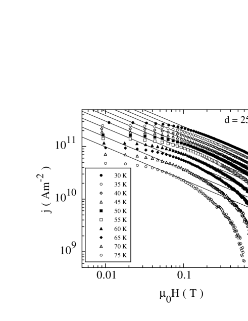
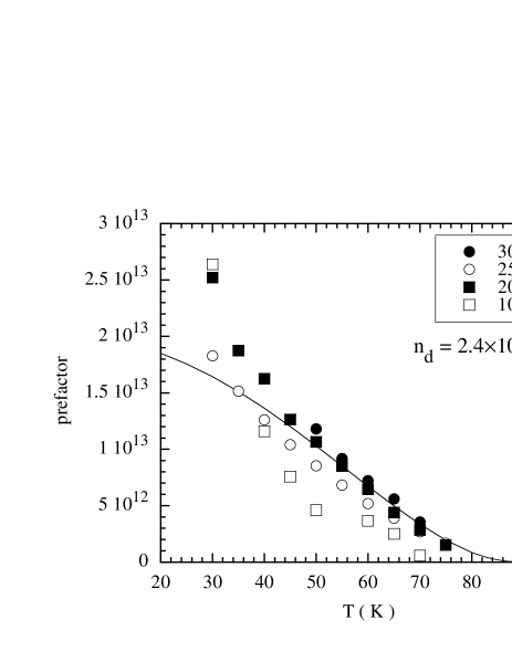
which shows data for the 250 nm–thick film. These are in every aspect representative of the data for all other films, and very similar to those found previously.[6, 10, 14] The sustainable current density shows a low–field plateau of constant current, followed by a smooth decrease of for fields higher than a given threshold. This decrease was recently interpreted in terms of creep of unpinned vortices through the forest of vortices presumably trapped on screw dislocation cores, a mechanism that ought to lead to a –dependence of the screening current density. However, the same field dependence is easily explained in terms of strong pinning, see Eqs. (16) and (19). The straight lines in Fig. 7 show fits to the –dependence predicted by Ovchinnikov and Ivlev; the power–law prefactors are given in Fig. 8. Adapting the same parameter values as for the fits to the zero-field current density, one sees that the temperature dependence of the prefactor withstands the comparison with the prediction (16) rather well. Again using the same parameters for the YBa2Cu3O7-δ material and the size of the Y2O3 inclusions, we obtain the drawn line of Fig. 8 for m-3, very close to the previously obtained values. While the temperature dependence predicted by Eq. (16) well matches the data at higher temperatures, it fails at temperatures below K, again indicating that pinning by other mechanisms may become important there.
Note that the field dependence of the sustainable current density does not follow a pure power law by any means, but gradually bends over from a –behavior to a dependence. This dependence is again in agreement with the strong pinning scenario: at high fields the vortex displacements due to pinning become comparable to the vortex spacing and the critical current density
starts do decrease more rapidly, as (Eq. (17)). The magnitude of the field at which this effect is expected is typically of the order 1 T.
V Discussion
The above results show that, even if perfect agreement is not found, strong pinning by Y2O3 inclusions can very well explain the large magnitude, as well as the temperature, field, and thickness dependence of the critical current density in laser ablated YBa2Cu3O7-δ films. The primary indication for this is the observed dependence on film thickness of the screening current density: first increases as function of film thickness before saturating at nm, and eventually slowly falling off again. This dependence is very similar to that measured by Jooss et al..[13] Other authors also report the increase of as function of film thickness , but with a maximum at nm followed by a much more rapid drop of .[15, 36, 37] Proposed explanations[15, 13] have been the increase of the effective penetration depth from towards for films thinner than ,[38] a bad film morphology and ill-connected islands for nm,[36] and differences in defect structure between the thinner and the thicker films.[37] We note that the fact that films from different sources display maximum for widely different film thicknesses, 100 nm and 250 nm respectively, exclude that the relative magnitude of and is at the origin of the increase of . However, our model explains this difference quite naturally in terms of Eq. (27) and the different density of second-phase inclusions in different films. An effective penetration depth would modify the current density obtained from pinning by thickness variations, but not the pinning force in the case of core pinning, for instance, by extended point defects or linear defects. The differences in optimal thickness also seem to exclude bad film morphology as an explanation: while such an effect may be likely for very thin films of thickness much less than 100 nm, it cannot explain an increase of up to nm. Finally, the role of deep trenches that modify the total current circulating in thin films[37] is excluded by the magneto-optical observations, which show homogeneous, featureless flux penetration. Thus, we conclude that the observed thickness dependence is in agreement with the scenario of strong pinning by extended point defects only.
Further evidence is the the lack of a cusp–like angular dependence of the critical current density for field aligned close to the film normal, which argues against a predominant role of extended line-like defects such as screw dislocation cores. The large difference between the algebraic temperature dependence of with the exponential dependence observed in clean YBa2Cu3O7-δ single crystals renders the relevance of weak collective pinning by oxygen vacancies unlikely. These observations gain in importance if we note that the field and temperature dependences reported here are observed in YBa2Cu3O7-δ films quite irrespective of the deposition method and conditions. While generally neglected, small Y2O3 inclusions are ubiquitous in YBa2Cu3O7-δ films deposited by different methods and may provide an explanation for both the magnitude and behavior of and the generality of this behavior. In our case, the defect density needed to explain the experimentally observed , m-3 means that the precipitates occupy between and of the sample volume. The of secondary phase material found in the X-ray analysis would be present as larger CuO2 outgrowths which do not pin vortices efficiently.
Strong pinning by larger point–like inclusions dominates over collective pinning by oxygen vacancies because thermal fluctuations in high temperature superconductors efficiently smear out the pinning potential of the vacancies.[35] Even at zero temperature it is energetically more favorable to pin a vortex on rather large inclusions than to have it lower its energy by wandering through the weak collective pinning landscape. Restricting ourselves to the single vortex limit, pinning on a large inclusion yields an energy gain ; this should be compared to the potential energy gain due to pinning by oxygen vacancies in the volume . Strong pinning by Y2O3 inclusions is more favorable if
| (29) |
where is the pinning energy gained in a correlation volume due to weak collective pinning by the oxygen vacancies and is the wandering exponent.[5] Substituting from Eq. (22), assuming for –pinning (pinning by mean free path fluctuations), and the oxygen ion radius m, we find that for physically allowable oxygen vacancy densities strong pinning by Y2O3 inclusions is always more favorable.
In the above, we have disregarded the effects of flux creep. While this can more or less be justified at low temperatures where creep rates are small, at higher temperatures flux creep certainly determines the observed sustainable current density. Experiments by Klaassen et al. [39] show that in the low–field regime of constant current density the activation energy for flux creep is of the order of 600 K; the activation barrier rapidly decreases and becomes constant at fields where decreases as function of . This low value of , much lower than the value predicted by nucleation-type creep models for depinning from linear extended defects,[20, 21] could be explained by the fact that vortices are held not by extended defects but by second-phase inclusions of much shorter longitudinal dimensions. The rapid decrease of the activation energy with magnetic field would be due to the decrease in the average number of defects, by which any given vortex line is effectively pinned (i.e. becomes of the order of the film thickness). The high–field regime of constant activation barrier can be explained if one assumes that there is less than one effective pin per vortex line; Our experimental result m-3 implies a distance between defects of the order 100 nm, comparable to both the smallest film thicknesses and the vortex spacing at T. So, indeed, in the field regime of decreasing , there is less than one effective defect per vortex, and the flux creep activation energy should be given by the energy barrier needed to break free a line from one defect. The power-law field dependence implies that the fraction of vortices pinned in this way suffices to keep the whole vortex lattice at rest; at the threshold (critical) current density, the entire vortex lattice depins until a vortex line is trapped by the next defect. Only at higher fields, where the experimental –data significantly deviate from a power–law, do we expect creep effects, vortex lattice shear, and plastic deformations of the vortex lattice to become important.
VI Conclusions
We have measured the dependence of the sustainable current density in pulsed-laser deposited YBa2Cu3O7-δ thin films on film thickness, field orientation and magnitude, and temperature. While the field and temperature dependence of the current density show the qualitative behavior often reported in literature for laser ablated, sputtered, and MO-CVD thin films, the film thickness dependence is consistent only with strong pinning by sparse large second phase inclusions (such as Y2O3). A model description of such pinning in different limits of flux line density and film thickness is consistent with the experimentally found behavior, if one assumes the inclusions to have the typical size nm3 obtained from previous TEM studies, [22, 25], with a defect density m-3. Such a defect density suggests in turn that at high fields, only a fraction of the vortices are pinned; these suffice to hold the entire lattice at rest until the critical current density is reached.
VII Acknowledgements
This work was partially supported by Polish Government grant No.” PBZ-KBN/013/T08/19. Support from French - Polish Programme “Polonium” and ESF “VORTEX programme is also gratefully acknowledged.
REFERENCES
- [1] B. Roas, L. Schultz, and G. Saemann-Ischenko , Phys. Rev. Lett.64, 479 (1990).
- [2] P.H. Kes, in Phenomenology and Applications of High Temperature Superconductors, Ed. K. Bedell et al., (Addison-Wesley, New York 1992).
- [3] R. Griessen, Wen Hai-hu, A.J.J. van Dalen, B. Dam, J. Rector, H.G. Schnack, S. Libbrecht, E. Osquiguil, and Y. Bruynseraede, Phys. Rev. Lett. 72, 1910 (1994).
- [4] A.I. Larkin and Yu. Ovchinnikov, Journ. Low Temp. Physics (1979)
- [5] G. Blatter, M.V. Feigel’man, V.B. Geshkenbein, A.I. Larkin, and V.M.Vinokur, Rev. Mod. Phys. 66, 1125 (1994).
- [6] H.R.A. Douwes, Ph.D. thesis, Leiden University, the Netherlands (1994).
- [7] P.H. Kes and C.C. Tsuei, Phys. Rev. Lett. 47, 1930 (1981). ibid. Phys Rev. B 28, 5126 (1983).
- [8] S. Kokkaliaris, A.A. Zhukov, P.A.J. de Groot, R. Gagnon, L. Taillefer, and T. Wolf, Phys. Rev. B 61, 3655 (2000).
- [9] M. Hawley, I.D. Raistrick, J.C. Beery, and R.J. Houlton, Science 251, 1587 (1991).
- [10] Ch. Gerber, D. Anselmetti, J.G. Bednorz, J. Mannhart, and D.G. Schlom, Nature 350, 280 (1991).
- [11] I.D. Raistrick and M. Hawley, in Interfaces in High Tc Superconductors, Springer (1993).
- [12] B. Dam et al., Physica C 296, 179 (1998); B. Dam, J.H. Rector, J.M. Huijbregtse, and R. Griessen, Physica C 305, 1 (1998).
- [13] Ch. Jooss, A. Forkl, R. Warthmann, H.-U. Habermeier, B. Leibold, and H. Kronmüller, Physica (Amsterdam) C 266, 235 (1996).
- [14] B. Dam, J.M. Huijbregtse, F.C. Klaassen, R.C.F. van der Geest, G. Doornbos, J.H. Rector, A.M. Testa, S. Freisem, J.C. Martinez, B.Staüble-Pümpin, and R. Griessen, Nature 399, 439 (1999).
- [15] F.C. Klaassen, Ph.D. thesis, Vrije Universiteit, Amsterdam (2002). F. C. Klaassen, G. Doornbos, J. M. Huijbregtse, R. C. F. van der Geest, B. Dam, and R. Griessen, Phys. Rev. B 64, 184523 (2001).
- [16] A. Wahl, V. Hardy, J. Provost, C. Simon, and A. Buzdin, Physica C 250, 163 (1995).
- [17] V. Hardy, S. Hébert, M. Hervieu, Ch. Simon, J. Provost, A. Wahl, and A. Ruyter, Phys. Rev. B 58, 15218 (1998).
- [18] C.J. van der Beek, M. Konczykowski, R.J. Drost, P.H. Kes, N. Chikumoto, and S. Bouffard, Phys. Rev. B 61, 4259 (2000).
- [19] R. Prozorov, E.B. Sonin, E. Sheriff, A. Shaulov, and Y. Yeshurun, Phys. Rev. B 57, 13845 (1998).
- [20] D.R. Nelson and V.M. Vinokur, Phys. Rev. Lett. 68, 2398 (1992).
- [21] D.R. Nelson and V.M. Vinokur, Phys. Rev. B 48, 13060 (1993).
- [22] T.I. Selinder, U. Helmersson, Z. Han, J.-E. Sundgren, H. Sjöström, and L.R. Wallenberg, Physica (Amsterdam) C 202, 69 (1992).
- [23] A. Catana, R.F. Broom, J.G. Bednorz, J. Mannhart, and D.G. Schlom, Appl. Phys. Lett. 60, 1016 (1992).
- [24] G. Kästner, D. Hesse, R. Scholz, H. Koch, F. Ludwig, M. Lorenz, and H. Kittel, Physica (Amsterdam) C 243, 281 (1995).
- [25] K. Verbist, A. Kühle, and A. Vassiliev, Physica (Amsterdam) C 269, 131 (1996).
- [26] Yu. N. Ovchinnikov and B.I. Ivlev, Phys. Rev. B 43, 8024 (1991).
- [27] In fact, evaluating the probability that a vortex line will encounter at least one defect overestimates the resulting critical current density . The real critical current lies between this and the product , where is the probability to encounter one pinning center only. This may explain why the experimental deviates downwards from a power-law behavior at high fields. An (incorrect) formula for that attempts to take this into account can be found in I. Abalosheva et al., Proceedings of the Second Euroconference on Vortex Matter in Superconductors , Physica (Amsterdam) C 369, 240 (2002).
- [28] A. Schönenberger, A. Larkin, E. Heeb, V. Geshkenbein, and G. Blatter, Phys. Rev. Lett. 77, 4636 (1996).
- [29] V.M. Vinokur, B. Khaykovich, E. Zeldov, M. Konczykowski, R.A. Doyle, and P.H. Kes, Physica C 295, 209 (1998).
- [30] M.V. Feigel’man and V.M. Vinokur, Phys. Rev. B 41, 8986 (1990).
- [31] L.A. Dorosinskiĭ, M.V.Indenbom, V.I. Nikitenko, Yu.A. Ossip’yan, A.A. Polyanskii, and V.K. Vlasko-Vlasov, Physica (Amsterdam) C 203, 149 (1992).
- [32] M. Konczykowski, F. Holtzberg, and P. Lejay, Superc. Sci. Tech. 4, S331 (1991).
- [33] J. Gilchrist and M. Konczykowski, Physica (Amsterdam) C 212, 43 (1993).
- [34] E.H. Brandt, M.V. Indenbom and A. Forkl, Europhys.Lett. 22, 735 (1993).
- [35] M.V. Feigel’man and V.M. Vinokur, Phys. Rev. B 41, 8986 (1990).
- [36] C.J. Liu, C. Schlenker, J. Schubert, and B. Stritzker, Phys. Rev. B 48, 13911 (1993).
- [37] E. Sheriff, R. Prozorov, Y. Yeshurun, A. Shaulov, G. Koren, and C. Chabaud-Villard, J. Appl. Phys. 82, 4417 (1997).
- [38] J. Pearl, Appl. Phys. Lett. 5, 65 (1964).
- [39] F.C. Klaassen, G. Doornbos, J.M. Huijbregtse, B. Dam, and R. Griessen, Physica (Amsterdam) C 341–348, 1463 (2000).