In-plane Tunneling Spectrum into a [110]-Oriented High- Superconductor in the Pseudogap Regime
Abstract
Both the differential tunneling conductance and the surface local density of states (LDOS) of a [110]-oriented high-temperature superconductor in the pseudogap (PG) regime are studied theoretically. As a competing candidate for the mechanism of PG state, the charge-density wave (CDW), spin-density wave (SDW), -density wave (DDW), and -wave superconducting (DSC) orderings show distinct features in the tunneling conductance. For the CDW, SDW, and DSC orderings, the tunneling conductance approaches the surface LDOS as the barrier potential is increased. For the DDW ordering, we show for the first time that there exist midgap states at the [110] surface, manifesting themselves as a sharp zero-energy peak in the LDOS, as in the case of DSC ordering. However, due to the particle-hole pair nature of the DDW state, these states do not carry current, and consequently the one-to-one correspondence between the tunneling conductance and the surface LDOS is absent.
pacs:
74.25.Jb, 74.50.+r, 74.20.MnOne of the most intriguing properties of high temperature superconductors is that, in the underdoped regime, the density of low-lying excitations is suppressed below a characteristic temperature , which could be well above the superconducting transition temperature Timusk99 . The origin for this so called pseudogap (PG) phenomenon remains unsettled. The existing scenarios for the mechanism of PG state include: the preformed pair model, where the Cooper pairs are formed above but either the phase associated with them fluctuates so strongly Emery95 or the coherence length (essentially the size of a Cooper pair) is so small Chen98 that the superconducting transition temperature is reduced from to ; stripes Zaanen89 ; Poilblanc89 ; Machida89 ; Emery90 ; Martin00 ; Castellani00 or antiferromagnetic fluctuations Pines97 , relying on the spin and/or charge fluctuations; spin-charge separation Lee99 , where the PG comes from the spinon sector; quantum criticality Sachdev99 , of which the -density wave (DDW) ordering breaking both time-reversal and translational symmetry Chakravarty01 and the circulating currents breaking time-reversal but preserving translational symmetry Varma99 , are the most representative models. Recently, several tunneling experiments have been proposed for both the preformed pair Choi00 ; Sheehy00 and antiferromagnetic correlation scenarios Bang00 . In this paper, based on a lattice model, we calculate the tunneling conductance, within the framework of a scattering approach, of a [110]-oriented normal-metal/underdoped high- superconductor junction. We typically consider the possible orderings: (i) the charge-density wave (CDW) to model the charge stripes; (ii) the spin-density wave (SDW) to model the spin stripes or antiferromagnetic correlations; (iii) the DDW state; (iv) the -wave superconducting (DSC) state. The exposure of distinct features among these orderings may help us pin down the mechanism for the PG. On the other hand, it has been predicted Hu94 that a sizable areal density of midgap states (i.e., states with essentially zero energy relative to the Fermi surface) exists on the [110]-oriented surface of a -wave superconductor. These states gives rise to a narrow surface local density of states (LDOS) peak at the Fermi energy, where the bulk density of states dips to zero. One of the consequences of these midgap states is a sharp zero bias conductance peak in single particle tunneling Tanaka95 ; Xu96 , which has been confirmed by several carefully controlled experiments Covington97 ; Alff97 ; Sinha98 ; Wei98 . A question arises naturally: Whether such kind of midgap states also exist in those normal-state orderings, and if so, how to distinguish them from those in the DSC ordering. This question constitutes another motivation for the present work. In light of this, we also calculate the LDOS near the [110]-oriented surface of the superconductor with all orderings listed above. We choose the [110] orientation, where the crystalline axis of the superconductor has a angle with respect to the direction normal to the surface, because the surface sensitivity of the electronic structure of some (e.g., the DDW and DSC) orderings can be manifested most pronouncedly in this setup.
The equation of motion for quasiparticles in a superconductor with a variety of orderings can be described in a unified manner by the generalized Bogoliubov-de Gennes equations defined in a two-dimensional tight-binding model:
| (1) |
Here the quasiparticle wavefunction comprises the electrons at energy with spin coupled with the holes of the same energy but opposite spin ; are the lattice indices in the coordinate system defined by the crystalline and axes (Hereafter the lattice constant is chosen to be unity); the single particle Hamiltonian , where is the nearest-neighbor hopping integral and or represent the relative position of those sites nearest neighboring to the th site; for the conventional CDW ordering while for the DDW ordering, represents the SDW order parameter; is the scattering potential to model the impurities, surface or interface. The quantity for the -wave superconducting order parameter while for the DSC order parameter. We note that the CDW, SDW, and DDW fields participate in the diagonal elements of the BdG matrix equations in spin space while the superconducting order parameter appears as off-diagonal elements. Of most interest to us in the present work, as explained above, we consider the tunnel junction comprising a normal metal on the left hand side and a superconductor on right hand side with a [110] oriented surface. We choose that the interface runs along the direction while the normal to the interface is parallel to the direction, along which the transport takes place. The insulating barrier at the interface is modeled by a scattering potential, . In addition, we assume that the order parameter is identically zero in the normal metal and constant in the superconductor. In general, due to the proximity effect, the order parameter is degraded when the interface is approached from the interface within a characteristic length. However, the discontinuity of the pair field remains at the interface and the physics discussed here is not changed qualitatively. By using the translation invariance of the system along the specular interface with spacing , the differential conductance (in units of the conductance quantum ) is calculated within the framework of the Blonder-Tinkham-Klapwijk (BTK) BTK82 theory:
| (2) |
where is the linear dimension of the junction along the direction, and are respectively the normal and Andreev reflection amplitude for a beam of electrons with spin incident from the normal metal at a fixed energy and the transverse wavevector with . We determine the values of and by matching the wavefunction. Away from the interface, the solution to the BdG equations consists of the incoming electron, reflected and transmitted electron and hole waves. The normalized zero-temperature tunneling conductance is defined as: , where with is the tunneling conductance through a normal junction of the identical interface condition. We remark that the BTK formula can be considered as an extended version of the Landauer-Büttiker Landauer70 formula for normal metal/superconductor junctions. The latter has found spectacular success in the description of quantum coherent transport in mesoscopic normal conductors. At the same time, we exactly diagonalize Eq. (1) to calculate the LDOS for a [110]-oriented surface of the superconductor, which is defined as:
| (3) |
where for a fixed value of , the summation is over the complete set of eigenstates.
Tunneling into CDW. In the case of normal-metal/CDW junction, the reflection amplitudes are obtained as:
| (4a) | |||||
| (4b) | |||||
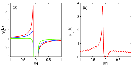
Notice that for the CDW, SDW, and DDW orderings (as considered below), the electron correlation is through the particle-hole channel so that the charge is conserved and the Andreev reflection process is absent. In Fig. 1(a), we show the tunneling conductance as a function of energy for various strength of the tunneling barrier. The surface LDOS is displayed in Fig. 1(b). As shown in Fig. 1, both the tunnel conductance and the LDOS vanish when the energy is below the energy gap . As the tunnel barrier becomes more opaque, the profile of the energy dependence of the tunneling conductance resembles that of the surface LDOS. Both and differ dramatically from those of a normal-metal/-wave superconductor junction BTK82 , by exhibiting no coherent peak at one of the gap edges. They are also asymmetric with respect to the Fermi energy . We also find the property that and , which show the strong dependence of both the tunneling conductance and LDOS on the macroscopic phase of the CDW.
Tunneling into SDW. In the case of normal-metal/SDW junction, we arrive at the reflection amplitudes as:
| (5a) | |||||
| (5b) | |||||
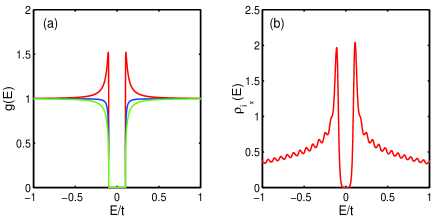
In contrary to the CDW case, where the spin is degenerate for the tunnel conductance, the reflection amplitude for the SDW is spin dependent. In particular, there holds the following symmetry property of the tunneling conductance between different spin bands: . It follows immediately that the total tunneling conductance is symmetric with respect to the Fermi energy, i.e., . As shown in Fig. 2, both the tunneling conductance and the LDOS vanishes when the energy below the energy gap . The profile of also resembles to that of as the strength of the tunnel barrier is increased. In addition, the coherent peak shows up at the gap edge in both and . Therefore, the overall behavior of the tunneling conductance of the N/SDW junction is qualitatively similar to the normal-metal/-wave superconductor junction.
Tunneling into DDW. In the case of normal-metal/DDW junction, the reflection amplitudes are obtained as:
| (6a) | |||||
| (6b) | |||||
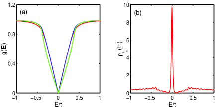
where . The energy gap for both the CDW and SDW ordering, as discussed above, is constant on the Fermi surface in the momentum space. The bulk energy gap of the DDW ordering is momentum-dependent, and of the form , which shows clearly that the DDW energy is closed along the nodal directions on the Fermi surface. In Fig. 3, we show the tunneling conductance of the N/DDW junction and the surface LDOS of the superconductor at the DDW state. Noticeably, a sharp peak appears at in the surface LDOS, which indicates the existence of the midgap states at the [110]-oriented surface of the DDW ordering. However, the tunnel conductance exhibits a V-shaped feature, which persists even when the tunnel barrier is opaque. The V-shape originates from the momentum dependence of the energy gap of the DDW ordering. In particular, the tunneling conductance does not show a zero-bias anomaly, it instead dips to zero. It can also be seen clearly that when , , which gives , regardless of the strength of the tunnel barrier. Therefore, in the tunneling limit, the profile of the conductance is strikingly different from the surface LDOS. Physically, the energy gap of the DDW ordering comes from the particle-hole pairs. In contrast to the superconducting state, there exists no Andreev reflection process to convert, at the interface, the single particle current into the supercurrent through the condensate, so that all quasiparticles with energy below the momentum-dependent DDW gap are completely reflected. Consequently, although there exist midgap states at the [110]-oriented surface of the superconductor in the DDW ordering, these states do not carry charge. However, as in the DSC case Zhu00 , the midgap states in the DDW state can also lead to a giant magnetic moment when a strong in-plane magnetic field is applied, the study of which is beyond the scope of current work. At this stage, we can conclude that no midgap states exist at the surface of the superconductor with either CDW or SDW ordering, but they really show up in the DDW ordering.
Tunneling into DSC. The tunneling conductance of normal-metal/DSC junctions, has been studied very intensively in the continuum model. Considering that the Andreev reflection process should take place even above in the preformed pair scenario, or in the spin-charge separation picture (where the spinons form -wave resonant-valence-bond state), we believe it is still helpful to present, within the lattice model, the results for the DSC case. We arrive at the reflection amplitudes:
| (7a) | |||||
| (7b) | |||||
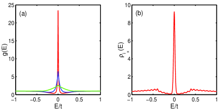
where . As shown in Fig. 4, the conductance at zero energy does not vanish. In particular, when the strength of the tunneling barrier is increased, a sharp peak occurs at zero energy in the conductance. In the opaque limit of the tunneling barrier, the profile of the conductance resembles that of the surface LDOS, which also exhibits a zero-energy peak, indicating the existence of midgap states. As we have emphasized above, the superconducting energy gap originates from the formation of Cooper pairs due to the electronic correlation in the particle-particle channel. Therefore, the charge is not conserved in a superconductor, and the Andreev reflection can happen in the interface between the normal metal and superconductor. It can be found from Eq. (7) that, at , and , regardless of the strength of the tunneling barrier. Therefore, the existence of the midgap states in the superconducting state corresponds to the perfect Andreev reflection process. In the phase fluctuation scenario, the long-range phase coherence is absent but the short-range correlation is still retained, the localized nature of the midgap states should be robust against the phase fluctuations. Therefore, if the phase fluctuation is the mechanism for the PG, we expect that the zero-bias conductance anomaly is still observable.
In summary, we have studied the tunneling conductance and the surface LDOS of a [110]-oriented high- superconductor in the underdoped regime. The distinct features among the different kinds of ordering—CDW, SDW, DDW, and DSC, are investigated. We have shown, in the opaque limit of the tunneling barrier, that: (i) for the CDW ordering, asymmetric tunneling conductance and surface LDOS with vanishing intensity within the gap; (ii) for the SDW ordering, symmetric tunneling conductance and surface LDOS with vanishing intensity within the gap; (iii) for the DDW ordering, V-shaped tunneling conductance but zero-energy-peaked surface LDOS; (iv) for the DSC ordering, zero-energy peaked tunneling conductance and surface LDOS. These different features can serve to distinguish the competing scenarios for the mechanism of the PG. We have also found the existence of surface midgap states in the DDW ordering, which is, to best of our knowledge, the first example occurring in a gapped normal system. Also in this case, the correspondence between the tunneling conductance and the surface LDOS is broken down.
Acknowledgments: The author thanks S. A. Trugman for helpful discussions. This work was supported by the Department of Energy through the Los Alamos National Laboratory.
References
- (1) For a review see, T. Timusk and B. Statt, Rep. Prog. Phys. 62, 61 (1999); B. Batlogg and C. M. Varma, Phys. World, February, 33 (2000).
- (2) V. J. Emery and S. A. Kivelson, Nature 374, 434 (1995).
- (3) Q. Chen, I. Kosztin, B. Janko, and K. Levin, Phys. Rev. Lett. 81, 4708 (1998); M. Randeria, cond-mat/9710223.
- (4) J. Zaanen and O. Gunnarsson, Phys. Rev. B 40, 7391 (1989).
- (5) D. Poilblanc and T. M. Rice, Phys. Rev. B 39, 9749 (1989).
- (6) K. Machida, Physica (Amsterdam) 158C, 192 (1989).
- (7) V. J. Emery, S. Kivelson, and H. Lin, Phys. Rev. Lett. 64, 475 (1990); V. J. Emery and S. Kivelson, Physica (Amsterdam) 209C, 597 (1993); V. J. Emery, S. Kivelson, and O. Zachar, Phys. Rev. B 56, 6120 (1997).
- (8) I. Martin, G. Ortiz, A. V. Balatsky, and A. R. Bishop, Int. J. Mod. Phys. B 14, 3567 (2000).
- (9) C. Castellani, C. DiCastro, M. Grilli, and A. Perali, cond-mat/0001231 (unpublished); R. S. Gonnelli, V. A. Stepanov, A. Morello, G. A. Ummarino, D. Daghero, L. Natale, F. Licci, and G. Ubertalli, cond-mat/0003100.
- (10) D. Pines, Physica (Amsterdam) 282-287C, 273 (1997).
- (11) For a review see, P. A. Lee, Physica (Amsterdam) 317-318C, 194 (1999).
- (12) S. Sachdev, Phys. World, April, 33 (1999).
- (13) S. Chakravarty, R. B. Laughlin, D. K. Morr, and C. Nayak, Phys. Rev. B 63, 094503 (2001).
- (14) C. M. Varma, Phys. Rev. Lett. 83, 3538 (1999).
- (15) H.-Y. Choi, Y. Bang, and D. K. Campbell, Phys. Rev. B 61, 9748 (2000).
- (16) D. E. Sheehy, P. M. Goldbart, J. Schmalian, A. Yazdani, cond-mat/0001039; D. E. Sheehy, I. Adagideli, P. M. Goldbart, and A. Yazdani, cond-mat/01060626.
- (17) Y. Bang and H.-Y. Choi, Phys. Rev. B 62, 11763 (2000).
- (18) C.-R. Hu, Phys. Rev. Lett. 72, 1526 (1994); Phys. Rev. B 57, 1266 (1998).
- (19) Y. Tanaka and S. Washiwaya, Phys. Rev. Lett. 74, 3451 (1995); S. Kashiwaya, Y. Tanaka, M. Koyanagi, and K. Kajimura, Phys. Rev. B 53, 2667 (1996).
- (20) J. H. Xu, J. H. Miller, Jr., and C. S. Ting, Phys. Rev. B 53, 3604 (1996).
- (21) M. Covington, M. Aprili, E. Paraoanu, L. H. Greene, F. Xu, J. Zhu, and C. A. Mirkin, Phys. Rev. Lett. 79, 277 (1997).
- (22) L. Alff, H. Takashima, S. Kashiwaya, N. Terada, H. Ihara, Y. Tanaka, M. Koyanagi, and K. Kajimura, Phys. Rev. B 55, 14757 (1997).
- (23) S. Sinha and K.-W. Ng, Phys. Rev. Lett. 80, 1296 (1998).
- (24) J. Y. T. Wei, N.-C. Yeh, D. F. Garrigus, and M. Strasik, Phys. Rev. Lett. 81, 2542 (1998).
- (25) G. E. Blonder, M. Tinkham, T. M. Klapwijk, Phys. Rev. B 25, 4515 (1982).
- (26) R. Landauer, Philos. Mag. 21, 863 (1970); M. Büttiker, Phys. Rev. Lett. 57, 1761 (1986).
- (27) Jian-Xin Zhu and C. S. Ting, Phys. Rev. B 61, 1456 (2000).