Electron Spin Injection at a Schottky Contact
Abstract
We investigate theoretically electrical spin injection at a Schottky contact between a spin-polarized electrode and a non-magnetic semiconductor. Current and electron density spin-polarizations are discussed as functions of barrier energy and semiconductor doping density. The effect of a spin-dependent interface resistance that results from a tunneling region at the contact/semiconductor interface is described. The model can serve as a guide for designing spin-injection experiments with regard to the interface properties and device structure.
pacs:
73.50.-h, 73.40.Qv, 73.30.+ySemiconductor device concepts that exploit the electron spin degree of freedom require an electrical means of injecting spin-polarized currents into a semiconductor. The two main experimental structures for meeting this requirement use injection from a ferromagnetic metal or from a spin-polarized semiconductor contact into a non-magnetic semiconductor. Such contacts are being studied both for their fundamental physics properties as well as for a range of technological possibilities reviewart . Measurements of spin-polarized electron injection are often made using a spin-LED configuration. In these experiments, electrons are injected into an n-type semiconductor from a polarized contact and are transported to a region in space, typically a quantum well, where they recombine with nominally unpolarized holes transported from an adjacent p-type doped region. The relative intensity of right- and left- circularly polarized light emitted from the quantum well gives a measure of the spin-polarization of the electron density in the recombination region. Recent measurements using injection from ferromagnetic contacts ploogmetal ; crowell ; jonkermetal and from spin polarized diluted magnetic semiconductors contacts jonkerhet ; molenhet have been reported.
Theoretical discussion of spin injection has centered around a conductivity mismatch between the contact and the semiconductor that can limit polarization of the injected carriers. These considerations were presented by Schmidt and coworkers schmidt . Smith and Silver smithsilver subsequently included the possibility of a spin selective interface resistance that results from tunneling and can improve spin injection. Rashba formulated the problem in terms of an injection coefficient in which currents dominated by tunneling at the interface can overcome the limitations of a conductivity mismatch rashba . These existing theories treat the contact and semiconductor simply as uniform conductive media and do not address critical issues of the real structures used in experiments which typically consist of a Schottky contact with band bending in a depletion region.
Here, we present a model of spin-polarized electron injection from a reverse-biased Schottky contact. We analytically solve spin-dependent continuity and drift-diffusion equations in the depletion region and examine the influence of the interface and the depletion region on the spin-polarized current and carrier densities in the semiconductor. We include the possibility of a spin selective interface resistance that results from tunneling processes at a ferromagnetic contact tunnel . We emphasize the important distinction between spin-polarization of the injected electron current and of the electron density. Even if an injected current is highly polarized it can result in small changes in the spin population of conduction electrons if the electron gas into which injection occurs has a high density or the magnitude of the injection current is small.
An energy diagram for a Schottky barrier, which includes the possibility of a narrow tunneling region near the interface, is shown in Fig. 1. A heavily
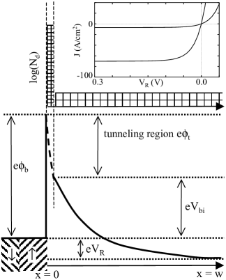
doped region near the interface, as illustrated by the doping profile in the upper panel of Fig. 1, can be designed to form a sharp potential profile through which electrons tunnel. The heavily doped region reduces the effective Schottky energy barrier that determines the properties of the depletion region sze . The total barrier e is divided into two parts, a tunneling region with barrier height e and an effective Schottky barrier height . The potential drop in the depletion region consists of the effective Schottky barrier height plus the applied reverse bias . Two parameters of the tunneling region, its tunneling resistance and the magnitude of the reduction of the effective Schottky barrier, can be separately controlled by the parameters of the doping profile, for example the height and width of the heavily doped region. The inset of Fig. 1 shows calculated current-voltage characteristics for two Schottky contacts with different bulk doping levels. Spin injection experiments are typically performed in reverse bias in which electrons are transported from the contact to the semiconductor.
The calculation decouples into a part for charge currents and densities and a part for spin currents and densities. The calculation for charge currents and densities is standard. We use a depletion approximation for the electrostatics and the diffusion/thermionic emission model for the electron current and density sze2 . We treat the spin current components using drift-diffusion equations
| (1) |
where is the current density, is the conductivity, and is the electrochemical potential for electrons of spin type ,. In the depletion region the conductivity varies with the local electron concentration . The contact and bulk semiconductor outside the depletion region are taken to be uniformly conducting and the electrochemical potentials relax to equilibrium in these extended regions according to where and is the spin-diffusion length in the contact or semiconductor. Because of the large electric field and rapidly varying electron density in the depletion region, a spin diffusion equation is not valid and we use spin-dependent continuity equations. Taking the difference in the continuity equations for the two spin types gives,
| (2) |
where is the spin lifetime in the semiconductor, is the intrinsic carrier density, and . The spin lifetime and spin diffusion length are related by . The electron mobility is and the appears because of particle conservation. Taking the difference in the drift-diffusion equations for the two spin types gives
| (3) |
Given that the electrostatic potential in the depletion region is quadratic, Eqs. 2 and 3 can be combined to give an equation of the form limitcase
| (4) |
where and are known constants that follow from the electrostatic solution in the depletion region. Eq. 4 can be transformed to a confluent hypergeometric equation by a change of variables and thus solved analytically in terms of two matching coefficients trans . These coefficients are determined by matching to the solutions for in the contact and in the charge-neutral region outside of the depletion region. Once the matching coefficients are known, the spin polarized currents and electron densities can be calculated. A spin-dependent interface resistance is incorporated to describe tunneling as in Ref. [smithsilver, ].
The model can be applied both to metal / semiconductor contacts and to heterojunction contacts with injection from a heavily doped, spin-polarized semiconductor into a less heavily doped unpolarized semiconductor with a higher energy conduction band awschalom . We first consider parameters appropriate to the heterostructure case. In Fig. 2 we show the calculated
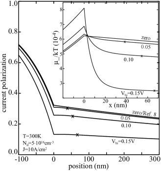
spin current polarization, , as a function of position for a series of structures with different barrier heights (negligibly small, 0.05, 0.1 and 0.15 eV), an injection current density of Acm-2, and a bulk doping of cm-3. The zero of position is the interface and the contact (semiconductor) at negative (positive) values of . The symbol x on the curves indicates the edge of the depletion region. Results from Ref. [smithsilver, ] for the same parameters are also shown. The contact is taken to be 95% spin polarized and with a conductivity twice that of the collecting semiconductor. It is assumed that the contact has a lower mobility but is more heavily doped than the collecting semiconductor so that depletion occurs in the collecting semiconductor. The interface resistance is zero. A mobility of =5000cm2/Vs, a spin diffusion length of 1m for the collecting semiconductor, and a spin diffusion length of 100nm in the contact at T=300K are used throughout the paper. The top two curves, which are indistinguishable, show the calculation for negligible barrier height and for the constant conductivity model of Ref. [smithsilver, ] which does not have a depletion region. In the limit of small energy barrier we recover the results of the constant conductivity model. There is a strong decrease in spin injection with increasing barrier height for fixed doping. The inset of Fig. 2 shows the difference in electrochemical potentials for spin-up and spin-down electrons, , as a function of position. As the barrier height increases there is a rapid drop in the difference in electrochemical potentials for spin-up and spin-down electrons across the depletion region. This rapid drop in across the depletion region is the cause of the decreased spin injection with increasing barrier height seen in the upper panel of Fig. 2. The drop results because the depletion region has a low and rapidly varying electron density.
The heterostructure situation depicted in Fig. 2 is somewhat idealized in the sense that spin polarized n-type semiconductor injectors that do not require high magnetic fields and low temperatures are still being sought. However, it is feasible to grow ferromagnetic metals on semiconductors, for example, epitaxial films of Fe on GaAs. In Fig. 3 we show the calculated
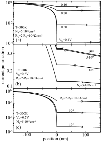
current spin-polarization as a function of position from a metallic contact (contact resistivity equal to 10-5cm). We have, for comparison purposes, computed all curves for 90% of the reverse saturation current density (which, of course, varies with barrier energy and bulk doping). In Fig. 3a we show, for fixed bulk doping (cm-3), current polarization curves corresponding to different effective barrier heights (0.1, 0.2, 0.3, and 0.4eV) and a spin-selective resistance at the interface of 10-3cm2 for spin-down current and half this value for spin-up current intres . A typical energy barrier for Fe/GaAs is e0.7eV and we have assumed a barrier lowering due to a heavily doped region near the interface. Fig. 3b shows an analogous series of curves for a fixed energy barrier (0.2eV) and different bulk doping densities (, , , and cm-3) with the same interface resistance. Fig. 3c shows a series of curves in which the barrier height (0.2 eV) and bulk doping (cm-3) are held fixed and the interface resistance is varied (, , cm2). From the results presented in Fig. 3, one sees that a depletion region is highly undesirable for spin injection. For efficient spin injection, the effective barrier height should not exceed about 0.2eV. Increasing the bulk doping improves the current spin-polarization because it reduces the width of the depletion region. It is also important to have a significant spin-dependent interface resistance. Spin injection is sensitive to the doping profile. To maximize spin injection, a heavily doped region near the interface should be used to reduce the effective energy barrier and form a spin-selective tunnel barrier to a ferromagnetic contact.
Current polarization is not the only important issue for spin injection experiments. A distinction should be made between the injected current polarization and the polarization of the electron density. In the spin-LED configuration, the observed degree of circularly polarized light is related to the spin-polarization of the electron density at the region in space where optical recombination occurs, typically in a quantum well. In Fig. 4a
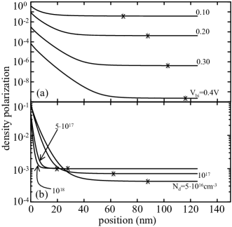
we show, for the device parameters used in Fig. 3a, the electron density spin-polarization as a function of position in the semiconductor for a series of barrier heights at fixed doping. Only for the smallest effective Schottky barrier is there a significant density polarization persisting tens of nm into the semiconductor. This is the region of interest for measurements of circularly polarized emission in the spin-LED configuration. Fig. 4b shows the effect of varying bulk doping on the density spin-polarization (parameters as for Fig. 3b). Even though both the injection current density and the current polarization efficiency increase with increased bulk doping concentrations, the higher density electron gas becomes more difficult to polarize. There is a point of diminishing returns on heavy bulk doping. To achieve significant electron density polarization in the optical recombination region, the density there should be as low as possible consistent with a small depletion region to ensure good spin injection efficiency and large injection currents.
We have presented a model for electrical spin injection at a Schottky contact between a spin-polarized electrode and a non-magnetic semiconductor. We have found that a significant depletion region at a Schottky contact is highly undesirable for spin injection. Design of the doping profile is very important to maximize spin injection. A heavily doped region near the interface can be used to form a sharp potential profile through which electrons tunnel and which also reduces the effective Schottky energy barrier that determines the properties of the depletion region. The doping profile should be chosen so that the potential drop in the depletion region is as small as possible, but the tunneling region must also have a significant interface resistance (of order 10-3cm2). Spin injection measurements using a spin-LED configuration are sensitive to the electron density polarization in the optical recombination region. The electron density in this recombination region should be as low as possible, consistent with a small depletion region, so that it can be more easily spin polarized.
Acknowledgment: We thank F. X. Bronold and I. Martin for helpful discussions. This work was supported by the SPINs program of the Defense Advanced Research Projects Agency.
References
- (1) See, e.g., S. A. Wolf, D. D. Awschalom, R. A. Buhrman, J. M. Daughton, S. von Molnár, M. L. Roukes, A. Y. Chtchelkanova, and D. M. Treger, Science 294, 1488 (2001) and references therein.
- (2) H. J. Zhu, M. Ramsteiner, H. Kostial, M. Wassermeier, H.-P. Schönherr, and K. H. Ploog, Phys. Rev. Lett. 87, 016601 (2001).
- (3) A. F. Isakovic, D. M. Carr, J. Strand, B. D. Schultz, C. J. Palmstrom, and P. A. Crowell, Phys. Rev. B 64, 016304 (2001).
- (4) A. T. Hanbicki, B. T. Jonker, G. Itskos, G. Kioseoglou, and A. Petrou, cond-mat/0110059.
- (5) B. T. Jonker, Y. D. Park, B. R. Bennett, H.-D. Cheong, G. Kioseoglou, and A. Petrou, Phys. Rev. B 62, 8180 (2000).
- (6) R. Fiederling, M. Keim, G. Reuscher, W. Ossau, G. Schmidt, A. Waag, and L. W. Molenkamp, Nature (London) 402, 787 (1999).
- (7) G. Schmidt, D. Ferrand, L. W. Molenkamp, A. T. Filip, and B. J. van Wees, Phys. Rev. B 62, 4790 (2000).
- (8) D. L. Smith and R. N. Silver, Phys. Rev. B 64, 045323 (2001).
- (9) E. I. Rashba, Phys. Rev. B 62, 16267 (2000).
- (10) See, for example, Y. Qi, Y. Xing, and J. Dong, Phys. Rev. B 58, 2783 (1998).
- (11) S. M. Sze, Physics of Semiconductor Devices, second edition (John Wiley & Sons, New York, 1981), p. 294.
- (12) See, e.g., Ref. [sze, ], pp. 248-260.
- (13) Eq. 4 can be shown to reduce to a spin diffusion equation in the limit of uniform carrier density, small electric field, and .
- (14) Let where . Then satisfies a confluent hypergeometic equation (CHE) and has a solution of the form where and are matching coefficients and and are independent solutions to the CHE.
- (15) Transport of electrons from a spin-polarized semiconductor into a larger bandgap semiconductor was reported by I. Malajovich, J. J. Berry, N. Samarth, D. D. Awschalom, Nature (London) 411, 770 (2001).
- (16) The interface resistance is small enough that it does not significantly effect the reverse bias current-voltage characteristics.