Nonlinear spin-polarized transport through a ferromagnetic domain wall
Abstract
A domain wall separating two oppositely magnetized regions in a ferromagnetic semiconductor exhibits, under appropriate conditions, strongly non linear I-V characteristics similar to those of a - diode. We study these characteristics as functions of wall width and temperature. As the width increases or the temperature decreases, direct tunneling between the majority spin bands reduces the effectiveness of the diode. This has important implications for the zero-field quenched resistance of magnetic semiconductors and for the design of a recently proposed spin transistor.
It has recently been reported that some doped semiconductors, such as Ga1-xMnxAs OhnoRTD and Ti1-xCoxO2 Matsumoto , undergo ferromagnetic transitions at temperatures as high as K and K respectively, while others (-doped Zn1-xMnxSe BeMnZnSe ) are almost completely spin polarized by the application of a relatively modest magnetic field. These findings have raised hopes for the realization of semiconductor-based magnetoelectronic devices review .
In a ferromagnetic semiconductor, the up- and down- spin components of just one carrier type are quite analogous to majority and minority carriers in ordinary doped semiconductors. Accordingly, a domain wall separating two ferromagnetic regions with opposite magnetizations is the analogue of a - junction, while two consecutive domain walls correspond to a -- transistor. In a recent paper FV we have exploited this analogy to show that nonlinear amplification of a spin-polarized charge current is indeed possible in the “--” configuration, and can be controlled by a magnetic field or a voltage applied to the “base” region between the two domain walls. However, the analysis of Ref. FV was based on the assumption that the probability of a carrier flipping its spin while crossing the domain wall is negligible. This corresponds to assuming the resistivity of the domain wall is large compared to that of the bulk material.
The resistance of a domain wall between ferromagnetic materials has been examined several times from different perspectives since the pioneering work of Cabrera and Falicov Falicov . These authors found that the resistance was very small, and later calculations Zhang ; Simanek have supported that result for metallic magnets. A far different regime is possible, however, when the spin polarization is or approaches . For example, experimental and theoretical resultsMathur indicate that domain walls in La0.7Ca0.3MnO3 may dominate the resistance in thin films. Magnetic semiconductor systems, due to their very small bandwidths, are also likely to be spin polarized, and thus their domain walls should be highly resistive in the absence of spin-flip transport processes across them.
A key question that has not been addressed so far is how the nonlinear current-voltage (I-V) characteristics of the domain wall are affected by spin-flip processes as the width of the domain wall increases. Note that the width of a domain wall can now be directly measured magneticSTM and, in principle, geometrically controlled Bruno . Our analytical theory of transport across the domain wall should therefore be useful in designing devices with optimal values of the controllable parameters. Certainly such a theory would be crucial to understanding the zero-field quenched resistance and the low-field magnetoresistance of magnetic semiconductors as well as to the realization of the “unipolar spin transistor” proposed in FV .
Here we present a quantitative study of the nonlinear I-V characteristics of a magnetic domain wall. The main issue is the competition between minority spin injection, which is responsible for the nonlinear spin-diode behavior, and majority spin transmission, which tends to suppress it. We shall show that the latter dominates when either the temperature is low, or the domain wall is thick. Assuming that the motion of carriers through the domain wall is ballistic, we derive analytic expressions for the charge and spin currents as functions of applied voltage, width of the domain wall, and temperature. We further identify a new transport regime for intermediate wall thicknesses, in which carriers are ballistically transported across the domain wall (characterized by nonlinear charge currents), but most spin polarization is lost.
Our model is schematically depicted in Fig. 1(a). The two ferromagnetic regions and are connected by a domain wall region of width , . The exchange field has the form
| (1) |
where , are unit vectors in the direction of and , and the angle varies linearly from in to in footnote1 .
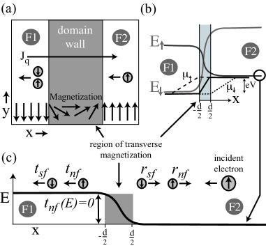
We assume that , while possibly large in comparison to a typical carrier wavelength, is smaller than the mean free path and the spin diffusion length , which is in turn smaller than the geometric size of the system. A charge current is injected from the left: our objective is to calculate the voltage that develops across the domain wall and the spin current due to the flow.
Let and be the quasi-chemical potentials, which control the nonequilibrium densities of majority and minority spin carriers respectively footnote2 . Far from the wall we have and the carrier densities have the equilibrium values and , with . Density variations from equilibrium are related to the difference of the quasichemical potentials near the domain wall. Since, by charge neutrality, we see that the relative change in the minority spin density is always much larger than the corresponding relative change in the majority spin density. This implies that is essentially pinned to its bulk value, while varies significantly in a region of length on either side of the domain wall. We can therefore set throughout and throughout , where is the electrostatic potential of relative to (see Fig. 1(b)) and the carriers are assumed to be electrons. The density variations are
| (2) |
where is the Boltzmann constant and is the temperature.
The charge currents for majority and minority spin orientations must satisfy the condition where the total charge current is independent of position. In addition, the minority carrier current is almost entirely a diffusion current, and is given by the classical relation , where is the diffusion constant. Because the spin density relaxes to equilibrium exponentially on the scale of ( i.e., where the lower sign holds in and the upper sign in ), the minority carrier current at can be written as , or, with the help of Eq. (2),
| (3) |
It will be argued below that for nondegenerate carriers the quasi-chemical potential of minority spin electrons on each side of the domain wall adjusts to the quasichemical potential of majority spin electrons on the opposite side, so that , (see Fig. 1(b)), and
| (4) |
Under the same assumption of nondegeneracy, it will also be shown that the matching condition for the spin current is
| (5) |
where , and and are population-averaged transmission coefficients, with and without spin flip (see Fig. 1(c)), which will be defined more precisely below. Thus, the spin current is conserved across a sharp domain wall (), but reverses its sign across a smooth one ().
Combining Eqs. (3-5), and using current conservation we arrive at our main results. First
| (6) |
where . For this reduces to the equation Streetman derived in (FV ), while for we get as expected for a ballistic conductor. In the linear regime this formula leads to the well-known interfacial resistance of Fert and Valet Fert . Second, in the immediate vicinity of the domain wall the spin current is given by
| (7) |
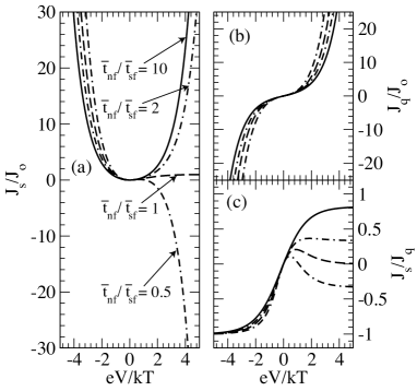
where the upper sign holds in and the lower sign in . We see that spin-flip processes cause the appearance of an odd-in-voltage component of the spin-current, whereas, for , the spin-current is an even function of FV . Shown in Fig. 2 is (a) the spin current in , (b) the charge current, and (c) the ratio of the two. The curves correspond to several different values of . The trends for the spin and charge current described above are evident in Fig. 2; specifically the charge current is always odd in whereas the spin current is even in the absence of spin-flip. When spin-flip dominates the spin current becomes odd as well. The spin current in is related to that in according to the following relation: . As becomes smaller, the “leakage current” between the two majority bands becomes significant, and the odd in term in the spin current begins to dominate. Over the entire range shown of the relationship between and is highly nonlinear indicating ballistic transport. Thus ballistic transport itself is not a sufficient condition for maintaining spin polarization in transport across a domain wall.
Assuming ballistic transport in the wall region, we calculate the transmission/reflection coefficients from the exact numerical solution of the Schrödinger equation
| (8) |
where is the exchange spin-splitting. The technique of solution is the same as used in Ref. Zhang . Sample results are shown in Fig. 3(a)-(c) for three different values of the dimensionless parameter , , and , corresponding to sharp, intermediate, and smooth domain walls respectively. smooth domain walls respectively. Recent experiments magneticSTM suggest the width of domain walls in artificial nanostructures can be as small as nm, giving for an effective mass equal to the electron mass and a spin splitting . Domain walls thinner than nm have already been inferred in thin GaMnAs layersSchiffer .
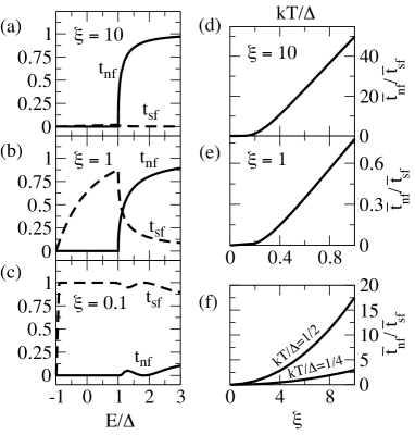
Fig. 3(d)-(f) shows the behavior of the key ratio as a function of temperature and thickness. As expected vanishes at low temperature, because, in this limit, there are no incident states above the exchange barrier to provide minority spin-injection. The spin diode is a thermally-activated device (as a - diode is), thus higher temperature is favorable to its performance. Fig. 3(d,e) supports this view by showing that minority spin injection only dominates above a certain temperature (depending on domain wall thickness). However the condition must be respected if the system is to be nearly spin-polarized. The conclusion is that there is a range in which unipolar spin diodes and transistors are expected to be operational.
We now come to the justification of the matching condition (5) and the calculation of the quasi-chemical potential offset. We begin with the former. In the spirit of the Landauer-Büttiker formalism we treat the ferromagnetic regions and as two reservoirs of spin polarized electrons at chemical potentials and which inject up- and down-spin electrons, respectively, in the domain wall region. The small density of minority spin carriers is neglected in the following argument. The components of the current due to electrons with energies in the range on the two sides of the domain wall are given (in units of ) by
| (9) |
where and are the non spin-flip and spin-flip reflection probabilities, related to and by the unitarity condition , and , are shorthands for the equilibrium distributions of majority spin carriers in and respectively. Note that, for nondegenerate carriers . We find that the spin-flip reflection coefficient is extremely small at all energies and thicknesses, and can therefore be safely neglected. With this approximation, combined with the unitarity condition, it is easy to show that the energy-resolved currents are given by . Noting that and integrating over energy we see that the total current is equal to where the average transmission coefficients are defined as
| (10) |
and is a constant. Similarly . The ratio is thus given by Eq. (5).
To justify the quasi-chemical potential offset condition, Eq. (4) we notice that the quasi-chemical potential of minority spin electrons near the left hand side of the domain wall is an average of the quasi-chemical potentials of right (+) and left (-) moving electrons : . (A similar relation holds for the quasi-chemical potential of minority spin electrons near the right hand side of the domain wall). The quasi-chemical potentials for right and left movers on either side are determined by the conditions of continuity
where and are the relative probabilities of transmission with and without spin flip respectively. The first of these equations, for example, says that the density of right-moving up-spin electrons of energy on the right hand side of the domain wall is equal to the density of right-moving down-spin electrons of the same energy which enter from the left and flip their spin, plus the density of right-moving up-spin electrons which enter from the left and do not flip their spin. Because the quasi-chemical potentials of the majority spin carriers are essentially pinned to their bulk values, we can set and . Integrating Eqs. (Nonlinear spin-polarized transport through a ferromagnetic domain wall) over energy, and making use of , we easily get and , as indicated in Fig. 1(b).
In summary, we have shown that both the thickness and the temperature have a profound influence on the nonlinear transport properties of a ferromagnetic domain wall. We have derived analytical formulas, Eqs. (6) and (7), for the charge and spin currents of this “magnetic junction” under physical assumptions similar to the ones from which the Shockley equations of a classical - junction are derived. These formulae indicate a new transport regime, where charge transport is ballistic, but spin polarization is lost. Equations (6) and (7), together with microscopic calculation of the population-averaged transmission coefficients, can be used to assess the effectiveness of unipolar spin-diode devices in realistic circumstances.
We gratefully acknowledge support from NSF grants No. DMR-0074959 and from DARPA/ARO DAAD19-01-1-0490.
References
- (1) H. Ohno et al., Appl. Phys. Lett. 73, 363 (1998); H. Ohno, Science 281, 951 (1998).
- (2) Y. Matsumoto et al., Science 291, 854 (2001).
- (3) B. Königet al. , Phys. Rev. B 60, 2653 (1999).
- (4) For a recent review of semiconductor spintronics see S. A. Wolf et al., Science 294, 1488 (2001) and references therein.
- (5) M. E. Flatté and G. Vignale, App. Phys. Lett. 78, 1273 (2001).
- (6) G. G. Cabrera and L. M. Falicov, Phys. Status Solidi B 61, 539 (1974); 62, 217 (1974).
- (7) P. Levy and S. Zhang, Phys. Rev. Lett. 79, 5110 (1997).
- (8) E. Simanek, Phys. Rev. B 63, 224412-1 (2001).
- (9) N. D. Mathur et al., J. Appl. Physics 86, 6287 (1999).
- (10) O. Pietzsch, A. Kubetzka, M. Bode, and R. Wiesendanger, Science 292, 2053 (2001); M. Pratzer et al., Phys. Rev. Lett. 87, 127201 (2001).
- (11) P. Bruno, Phys. Rev. Lett. 83, 2425 (1999).
- (12) This model describes a Neél wall in a ferromagnetic film in the x-y plane. With the slight change the model also describes a Bloch wall.
- (13) The exact electronic states are, strictly speaking, neither “up” nor “down” with respect to the local magnetization, but superpositions of the two orientations. However, the relative phase of the up and down components of the wave function has a rapid spatial variation — typically on the scale of the electronic wavelength . Therefore transverse spin coherence disappears on a scale larger than , and the carriers’ spin can be safely assumed to be either parallel or antiparallel to the local magnetization.
- (14) B. G. Streetman and S. Banerjee, Solid State Electronic Devices (Prentice Hall, 2000), Chapters 5,7.
- (15) T. Valet and A. Fert, Phys. Rev. B 48, 7099 (1993).
- (16) S. J. Potashnik, K. C. Ku, R. Mahendiran, S. H. Chun, R. F. Wang, N. Samarth, P. Schiffer, and M. Jaime, unpublished.