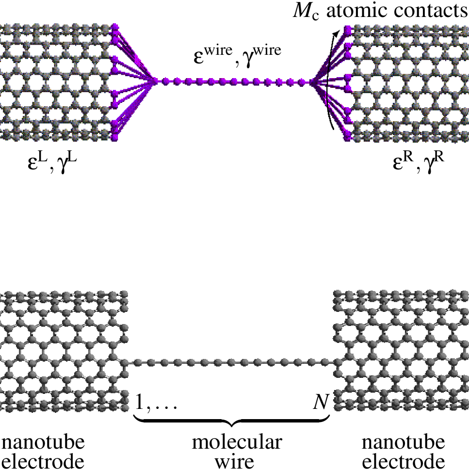
Molecular wire-nanotube interfacial effects on electron transport
Abstract
We discuss the conductance of a molecular bridge between mesoscopic electrodes supporting low-dimensional transport and bearing an internal structure. As an example for such nanoelectrodes we assume semi-infinite (carbon) nanotubes. In the Landauer scattering matrix approach, we show that the conductance of this hybrid is very sensitive to the geometry of the contact unlike the usual behaviour in the presence of bulk electrodes.
pacs:
PACS numbers: 73.50.-h, 73.61.Wp 85.65.+h2
The urge for smaller, faster, and cheaper electronic devices drives a race of increasing pace for the miniaturisation of transistors. Such an activity has provided an interplay between fundamental and applied research giving rise to the fields of mesoscopic and nano physics. The principal ideas are based on the ‘top-down’ miniaturisation of electronic devices to micro- or nanometre-size and the exploitation of nontrivial quantum effects in solid state physics at these length scales. An arena closely related to mesoscopics is molecular electronics [1]. As in mesoscopic systems, quantum mechanical methods need to be accommodated as compared to the conventional description of electronic devices. In addition, a detailed microscopic analysis of the physical objects involved should be included since part of the challenge is to use individual molecules or supramolecular structures as (reproducible) circuit elements. This is the ‘bottom-up’ manufacture philosophy.
Since the original proposal of a molecular rectifier [2] significant progress on transport across a single molecule has been demonstrated experimentally only in recent years. This owes to the advances in self-assembly techniques, end-group modifications, scanning probe and break-junction techniques, which allow atomic-scale control and positioning of single molecules and their assemblies. As a result, a series of electron transport measurements through molecular complexes between metallic pads has been reported [3, 4].
Such experiments complemented by theoretical efforts have pointed out a number of factors that determine the conductance in such structures [3, 4, 5, 6, 7, 8, 9]. The most important include the molecular electronic structure related to the resonant spectrum and the distribution of the wavefunction along the bridge, the location of the electrodes equilibrium Fermi energy with respect to the molecular electronic spectrum, charging effects, the electron-phonon coupling in wires of low conduction, and the interface between electrodes and molecular complexes. Many of these effects are inter-related but the classification helps in understanding the basic underlying transport mechanisms.
In this paper, we focus on the effect of the molecular wire-electrode interface on electron transport. In a typical experimental setup a molecular bridge connects two electrodes acting as electron donor and acceptor reservoirs. Despite this conceptual separation of the molecular device into its constituents what is measured is the conductance across the whole system. This implies that besides the intrinsic molecular ability to convey charge the coupling of the molecular complex to the environment is significant. This argument is supported by theoretical work which shows the need for an atomistic description [8, 9].
Moreover, in theoretical studies one usually assumes the molecular wire attached to one dimensional or bulky electrodes [5, 6, 7, 8, 9]. Both are described by a smooth local density of states, whereas, the latter bear also a continuum of possible conducting channels. But none of these conditions may hold in general. For example such a description is inadequate for experiments employing scanning tunnelling microscope tips where interface-induced effects have been found to strongly influence the measured conductance [10]. The tip electronic structure, which is determined by either structural formation or adsorbates, gives rise to characteristic signatures. To account for such effects one may study the conductance across a cluster which includes the molecule and the tip [8]. In contrast to previous studies we assume carbon nanotubes which exemplify the contrary of both aforementioned features. Apart from being an ideal example, carbon tubules are also promoted as electrodes with lateral dimensions comparable to the size of the molecular connector. Our final aim is to both point out the basic issues and understand how to manipulate the contact in order to achieve control over electron transport.
Carbon nanotubes support up to two channels for electrons with energy around the equilibrium Fermi energy and have a complex topology. They are known to exhibit a wealth of properties depending on their diameter (), chirality (orientation of graphite sheet roll up), and whether they consist of a single cylindrical surface (single-wall) or more (multi-wall) [11]. Carbon tubules are defined by a pair of integers denoting the chiral vector. First experiments to build nanotube-supramolecule-nanotube hybrids have been attempted [12]. Furthermore, carbon nanotubes are already utilised as scanning probe tips to study molecular structures [13].
In what follows, we show that electron transport shares distinct properties depending on the number of atomic contacts at the interface between the molecular bridge and the electrodes. It also depends on the symmetry of the channel wavefunctions transverse to the transport direction. We demonstrate that single-atom contacts give rise to complex conductance spectra exhibiting quantum features of both the molecule and the electrodes. These are attributed to the electronic structure of the molecular wire and to the local density of states of the leads, respectively. Multiple contacts provide a mechanism for transport channel selection, leading to a scaling law for the conductance and allowing for its control. Channel selection also highlights the role of molecular resonant states by suppressing details assigned to the electrodes.
We first give specific details of the system we study. The electrodes are open-ended single-wall carbon nanotubes taken as either armchair or zigzag type. The latter are defined by the and chiral vectors, respectively. For the description of the electronic spectrum we use a parametrised tight-binding Hamiltonian with a -electron per atom [11]. This ignores curvature induced effects but takes into account all qualitative features. Reflecting our aim to provide a qualitative understanding of the phenomenology of the physical problem, the molecular wire is also modelled at the tight-binding level by taking a dimerised chain of atomic sites [7]. This is represented by an alternating nearest-neighbour interaction between subsequent pair of atoms. The ratio of the coupling strengths determines the dimerisation parameter. Such a system bears two electronic bands, whereas the width of the bands and the corresponding gap are determined by the hopping terms.
The electronic Hamiltonian of the system, including the left (L) and right (R) tube (see Fig. 1), reads
| (1) | |||||
| (2) | |||||
| (3) | |||||
| (4) |
Here, ( eV), (), and denote nearest-neighbour hopping terms between atoms of the left or right carbon tubule leads, molecular bridge, and the bridge/lead interface, respectively. We shall leave unspecified for it does not influence the qualitative behaviour we point out below. Effects related to the exact magnitude of the interfacial coupling strength have been described elsewhere [14]. Note that the dimerisation parameter of the wire which is defined as the absolute value of the difference between the alternating bonds over the average coupling strength has been fixed to around . Our parametrisation sets the band gap and each bandwidth of the molecular wire to 2 and 3 eV, respectively. For simplicity, all on-site energies have been fixed to zero implying that the symmetric band structures of both the carbon nanotubes and the dimerised chain are centred at zero. In Eq. (1), is a two-dimensional coordinate spanning the tube lattice. Summations over and run over interfacial end-atoms of the leads. In general, there are such atomic positions, depending on the perimeter of the tubes, and a number of hybridisation contacts ranging from a single contact (SC), to multiple contacts (MC).
We also use a square lattice model of mesoscopic electrodes with nearest-neighbour interactions (eV) and periodic boundary conditions on the longitudinal cuts parallel to the lattice bonds. Although this model may be unphysical or at least very difficult to realise experimentally [15], it is instructive upon comparison and delivers additional analytic insight [16].
For solving the transport problem we use the Landauer theory [17] which relates the conductance of a system to the electron transmission probability in the single-particle approximation [18]. This approach successfully accounts for unique quantum effects in mesoscopic systems [19]. The electron wavefunction is assumed to extend coherently across the device and the two-terminal, linear-response conductance at zero temperature reads
| (5) |
The factor accounts for spin degeneracy, and is the energy-dependent total transmittance for injected electrons with Fermi energy . The transmission function is given by , where are quantum numbers labelling open channels for transport which belong to mutually exclusive leads. In our case these are the two semi-infinite perfect nanotubes. The attached molecular system defines a scattering problem, and is the corresponding quantum-mechanical scattering matrix.
We determine the central quantity, , numerically by employing an efficient algorithm for calculating the Green function for arbitrary tight-binding Hamiltonians. The -matrix is computed from the Green function via the Fisher-Lee relation [19]. This general scattering technique has been recently formulated for studies of the giant magnetoresistance and is described in detail in Ref. [20]. It was later applied to a number of problems including the electric conductance in multi-wall carbon nanotubes [21]. The computational scheme proceeds at three stages: a) the calculation of an effective (renormalised) interaction between the electrodes by projecting out the degrees of freedom of the scatterer, b) the computation of the Green function in the absence of the scatterer, and c) the use of the Dyson equation to express the required Green function of the composite system (leads plus scatterer).
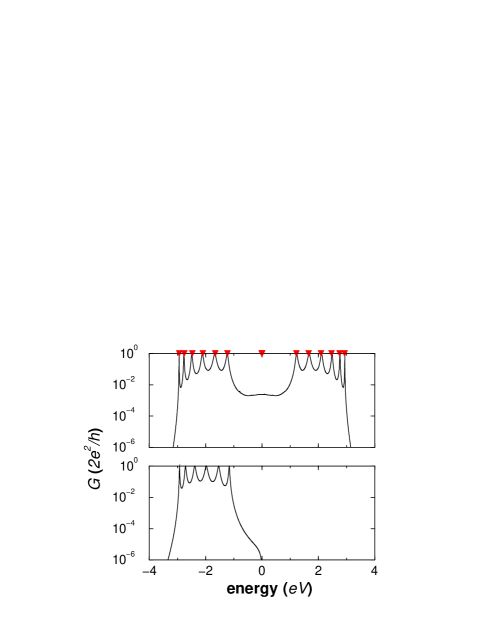
Typical conductance spectra for the two extreme examples of a single interfacial atomic contact and multiple contacts are shown in the left and right panel of Fig. 2, respectively. One observes the general resonant character of transport typical of mesoscopic systems. In particular, the conductance shows resonances of quantum unit () height at eigenenergies close to that of the energy spectrum of the isolated molecular chain which is indicated by symbols [22]. They arise because of back reflections at the molecular wire-electrode interface. In the SC-scenario all open channels contribute to the transmission, i.e. is non-zero for any . For carbon tubule leads (upper right panel of Fig. 2) we observe additional structure in the conductance spectra. Additional results show that distinctive features such as antiresonances reflect the local density of states of the carbon nanotubes and are signatures of van Hove singularities in the carbon tubules band structure [23]. Due to the simplicity of our model no antiresonances from the electronic molecular structure can occur [24].
The MC-configuration exhibits a profoundly different behaviour. The conductance vanishes for part of the spectrum for both square lattice tubes and carbon tubules as shown in the lower panels of Fig. 2. In addition, the quantum features associated to the carbon nanotube structure disappear. The complicated conductance spectrum appears now as a series of resonant peaks. Detailed analysis of the -matrix elements revealed that only wavefunctions of the tubes without modulation along the cross-section circumference allow for transport, thereby, yielding the zero conductance when such channels are not available. Evidently, this leads to asymmetric conductance spectra in general. We may say that the MC-configuration acts as a channel filter. The selection is a consequence of a sum rule that determines the transmission of each open channel and is related to the spectral density [9]. It may be viewed as the wavefunction overlap (see Eq. (1), due to the nature of coupling only the transverse profile is important) and, hence, from symmetry considerations it is clear that the channel selection is a generic feature of cylindrical electrodes. It follows that channel filtering should approximately prevail also for non-cylindrical, mesoscopic electrodes with lateral confinement. This has been observed in additional calculations.
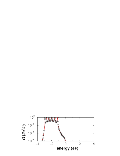
A further particular feature of the MC configuration is that the conductance obeys a scaling law. That is, , where is the diameter of the tube (Fig. 3). This is a mere contact effect related to the symmetry of the contributing channel wavefunction that should hold for any effective coupling with the form considered here and for any kind of tubule electrode. We can give a qualitative argument by inspection of the resonant structure of the conductance spectrum. In a linear-linear plot we see a series of Lorentzian peaks. According to Breit-Wigner such peaks scale as the square of the coupling strength times the local density of states. The effective coupling scales as times . The latter relates to the diameter of the tube. Taking into account the single-channel transport and the fact that the transverse profile of the contributing channel wavefunction has no nodes and is normalised, one arrives at a local density of states proportional to which fixes the scaling law. A more rigorous analysis shows that the conductance depends only on via a non-zero molecular wire self-energy induced by the electrodes [5, 16]. The exact form of the scaling law readily follows by repeating the above argument.
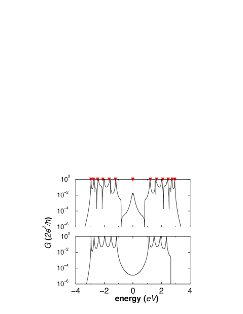
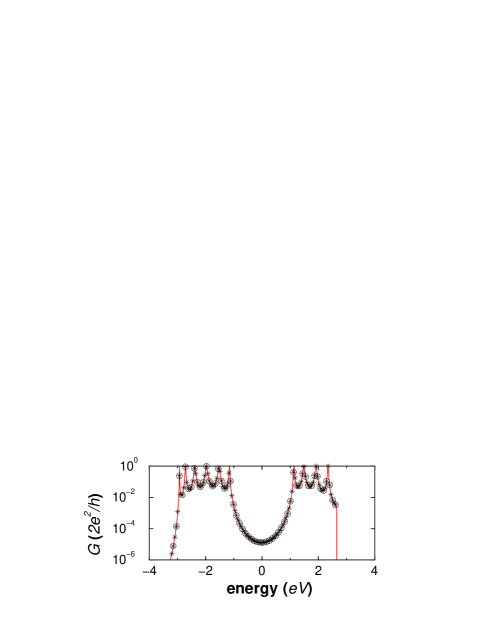
More generally, multiple contacts allow for control of low-dimensional transport via channel selection with the ‘intermediate contact’ case, i.e. , exhibiting much richer behaviour. This results from a combination of the effects we described hitherto. For completeness we discuss a specific example which supports channel selection and illustrates once more the importance of the interface in molecular system-nanoelectrode hybrids. In Fig. 4 typical conductance spectra for zigzag carbon nanotube electrodes are shown. To interpret these results we note that transport usually takes place at eV around the Fermi energy . For this part of the spectrum apart from the tunnelling nature of the conductance owing to the gap of the dimerised chain, we notice a complete suppression of conductance for , due to contact ‘dimensionality’ [25]. The origin of this effect derives from metallic zigzag nanotubes supporting two degenerate transport channels in this energy region with an antisymmetric wavefunction within a cell consisting of three atomic sites (along the circumference of the tubule). Hence, the wire/tube overlap gives a zero contribution for as depicted and non-zero otherwise [26].
In summary, we have studied interfacial effects on the conductance of a hybrid built by a molecular wire coupled to low-dimensional leads. We have pointed out immediate consequences of the contact geometry and dimensionality on electron transport across such systems. These include the possibility of channel selection and the existence of a scaling law for devised geometries. Although we presented results for a dimerised chain such effects are generic. We also demonstrated that a square lattice tube model for electrodes exhibits the above features. However, replacement by natural and realistic candidates of molecular electronic circuits, carbon nanotubes, adds richer structure to the conductance profile. This is related to the tubule topology which determines the local density of states. A complementary study of such effects should take into account a full microscopic description of the molecular system including structural relaxation and carbon nanotube caps. Another possibility is to consider multi-wall nanotube leads. In this case, an axial magnetic field of reasonable magnitude can be applied which modulates the symmetry of the tube states and, hence, can act as an external tuning parameter. But perhaps the most challenging task would be to discuss electron transport for finite temperatures and bias voltages, phase-breaking mechanisms, and charging effects and see how the above features are modified.
We would like to thank the organisers of the ‘Molecular Electronics 2000’ conference for giving us the opportunity to present this work. We also thank A. Bachtold, C.J. Lambert, and S. Sanvito for comments and discussions. G.F. acknowledges support by P. Fulde for participation at this conference.
REFERENCES
- [1] Molecular Electronics: Science and Technology, edited by A. Aviram and M.A. Ratner (New York Academy of Sciences, New York, 1998); C. Joachim, J.K. Gimzewski, and A. Aviram, Nature (London) 408, 541 (2000); A. Nitzan Annu. Rev. Phys. Chem. 52, 681 (2001).
- [2] A. Aviram and M.A. Ratner, Chem. Phys. Lett. 29, 277 (1974).
- [3] M.A. Reed et al., Science 278, 252 (1997); C. Kergueris et al., Phys. Rev. B 59, 12505 (1999); C. Joachim, J.K. Gimzewski, R.R. Schlittler, and C. Chavy, Phys. Rev. Lett. 74, 2102 (1995); W. Tian et al., J. Chem. Phys. 109, 2874 (1998); L. Venkataraman and C.M. Lieber, Phys. Rev. Lett. 83, 5334 (1999).
- [4] E. Braun, Y. Eichen, U. Sivan, and G. Ben–Yoseph, Nature 391, 775 (1999); H. Fink and C. Schönenberger, Nature 398, 407 (1999); D. Porath, A. Bezryadin, S. de Vries, and C. Dekker, Nature 403, 635 (2000).
- [5] V. Mujica, M. Kemp, and M.A. Ratner, J. Chem. Phys. 101, 6849 (1994).
- [6] M.P. Samanta et al., Phys. Rev. B 53, R7626 (1996); M. Magoga and C. Joachim, Phys. Rev. B 56, 4722 (1997); M.D. Ventra, S.T. Pantelides, and N.D. Lang, Phys. Rev. Lett. 84, 979 (2000); N.D. Lang and P. Avouris, Phys. Rev. Lett. 84, 358 (2000); V. Mujica, A.E. Roitberg, and M.A. Ratner J. Chem. Phys. 112, 6834 (2000).
- [7] C. Joachim and J.F. Vinuesa, Europhys. Lett. 33, 635 (1996).
- [8] E.G. Emberly and G. Kirczenow, Phys. Rev. B 58, 10911 (1998); ibid 60, 6028 (1999).
- [9] S.N. Yaliraki and M.A. Ratner, J. Chem. Phys. 109, 5036 (1998).
- [10] A.L. Vázguez et al, Phys. Rev. Lett 80, 357 (1998); A.I. Onipko et al, Phys. Rev. B 61, 11118 (2000).
- [11] R. Saito, G. Dresselhaus, and M.S. Dresselhaus, Physical Properties of Carbon Nanotubes (Imperial College Press, London, 1998); P. McEuen, Physics World 13, 31 (2000).
- [12] A. Bachtold (private communication).
- [13] S.S. Wong et al., Nature 394, 52 (1998).
- [14] G. Fagas, G. Cuniberti, and K. Richter, Phys. Rev. B 63, 045416 (2001).
- [15] It may however be of relevance to the structures described in O.S. Schmidt and K. Eberl, Nature 410, 168 (2001).
- [16] G. Cuniberti, G. Fagas, and K. Richter, unpublished.
- [17] Y. Imry and R. Landauer, Rev. Mod. Phys. 71, S306 (1999).
- [18] Another theoretical approach, widely used in studies of electron transport across molecular junctions, has its roots in the transfer Hamiltonian method [5]. Nevertheless, it has been recently shown that the two approaches are in agreement, see L.E. Hall, J.R. Reimers, N.S. Hush, and K. Silverbrook, J. Chem. Phys. 112, 1510 (2000).
- [19] S. Datta, Electronic Transport in Mesoscopic Systems (Cambridge University Press, Cambridge, 1995); D.K. Ferry and S.M. Goodnick, Transport in Nanostructures, (Cambridge University Press, Cambridge, 1997).
- [20] S. Sanvito, C.J. Lambert, J.H. Jefferson, and A.M. Bratkovsky, Phys. Rev. B. 59, 11936 (1999).
- [21] S. Sanvito, Y.-K. Kwon, D. Tománek, and C.J. Lambert, Phys. Rev. Lett. 84, 1974 (2000); this reference includes suggestions for the implementation and computation of the exact Green function of the tubules.
- [22] With increased resolution one sees that there are two eigenenergies lying symmetrically to zero energy which are present only in the case of open boundary conditions. They correspond to states with identical probability densities peaked at the chain end-atoms and suppressed elsewhere explaining the tunnelling nature of the conductance.
- [23] G. Cuniberti, G. Fagas, and K. Richter, Acta Phys. Pol. B 32, 437 (2001).
- [24] E. Emberly and G. Kirczenow, Phys. Rev. Lett. 81, 5205 (1998).
- [25] The position of the contacts does not influence conductance for zigzag carbon tubule leads, while for armchair carbon tubules there is no distinction only if is odd. This is explained by the structure of the carbon nanotube unit cell.
- [26] For armchair carbon tubules, conductance is always finite but for even, only one channel instead of two is contributing. Arguments similar to those given for zigzag nanotubes hold.