Effect of disorder on the conductance of a Cu atomic point contact
Abstract
We present a systematic study of the effect of the disorder in copper point contacts. We show that peaks in the conductance histogram of copper point contacts shift upon addition of nickel impurities. The shift increases initially linearly with the nickel concentration, thus confirming that it is due to disorder in the nanowire, in accordance with predictions. In general, this shift is modelled as a resistance which is placed in series with the contact resistance . However, we obtain different values for the two peaks in the histogram, being larger for the peak at higher conductance.
I Introduction
Quantum point contacts (QPC’s) are constrictions in a conducting material whose size is of the order of the Fermi wavelength of the electrons. The first quantum point contacts were fabricated in a 2-dimensional electron gas (2DEG) in a semiconductor heterostructure PRL_vanwees88 ; JPC_Wharam88 . Their conductance exhibits a series of steps as a function of constriction size. The plateaus in between these steps are positioned at integer multiples of (12.9 k)-1, the quantum of conductance. This phenomenon is explained as a consequence of the quantization of the electronic energy levels, resulting from the confinement of the electrons in the direction perpendicular to the current. Signs of quantized behavior were also seen in the conductance of quantum point contacts made from metals PRB_Krans93 ; PRL_Pascual93 ; PRL_Olesen94 . When a thin metallic wire is slowly broken, its conductance as a function of contact size shows smooth plateaus, alternated by steps of the order of . In this case, however, the plateaus are not necessarily horizontal or positioned at integer multiples of . Moreover, when the two wire ends are pressed together and broken again, the precise shape of the trace differs from trace to trace. In order to obtain fully reproducible results, a histogram is often created by projecting each conductance trace onto the conductance axis and adding the contribution of several thousands of traces. For many metals, the histograms show well-defined peaks which represent preferred conductance values.
The physical origin of these peaks has been debated heavily PRL_Yanson97 , especially the question whether they are indeed related to the quantization of electronic energy levels or rather to the discrete and abrupt changes in the cross-sectional area of the nanowires, which are caused by the fact that the contact must change its size by at least one, discrete, atom. It was shown both experimentally, by force measurements PRL_Rubio96 , and theoretically, by numerical simulations PRL_Sutton93 , that steps are correlated with atomic rearrangements of the contact. Thus, plateaus in the conductance traces correspond to stable atomic configurations. Apart from its geometry, the conductance of such a configuration is determined by the conductance of individual atoms of the metal under investigation. It was shown Nature_Scheer98 that the conductance of a one-atom point contact is governed by the nature of its valence orbitals. For monovalent s-metals such as Na, Cu or Au, a one-atom contact has a conductance of nearly 1 . On the other hand, transition metals such as Ni, Pd or Pt, which have d-valence orbitals, have a one-atom conductance of the order of 1.6 .
In experiments on both semiconductor QPC’s PRL_vanwees88 and QPC’s made of monovalent s-metals it has been observed that the quantization of the conductance is never perfect: the peaks in the histograms are shifted below quantized values ( = 1, 2, 3 ). In metallic point contacts, such a shift has been observed in gold PRB_Costa-Kramer97 ; PRB_Hansen97 , sodium Nature_Krans95 , silver PRB_Hansen97 and copper PRB_Hansen97 . Two possible origins of the shift have been discussed in the literature. It has been attributed to disorder either in the leads to the contact PRL_vanwees88 , or in the contact itself PRL_Garcia97 ; PRB_Brandbyge97 ; PRB_Burki99 . In all cases, a model was adopted in which the shift is accounted for by an ‘extra’ resistance that is placed in series with the true contact resistance . is assumed to be an exact integer multiple of , and it is then straightforward to determine from the histograms. Typical experimental values are 400 for a 2DEG PRL_vanwees88 , 100 for sodium Nature_Krans95 , 100-500 for gold PRB_Costa-Kramer97 ; PRB_Hansen97 , 500 for silver PRB_Hansen97 and 700 for copper PRB_Hansen97 .
In all theoretical studies into disorder in QPC’s, adding disorder resulted in a downshift and smearing of the peaks in the conductance histogram. In the work of García-Mochales et al. PRL_GarciaMochales97 , for example, the nanowire was simulated by a tight binding model. The disorder is introduced by random on-site energies, while the overlap between atomic orbitals is described by a hopping term between sites. The conductance was calculated as a function of the Fermi energy, while the geometry was kept constant. A histogram was then constructed, which showed peaks that were indeed shifted. The series resistance (calculated by fitting the best resistance value centering simultaneously all peak maxima at the corresponding integer values of ) were found to range from about 10 for small disorder to 1000 for large disorder.
Bürki et al. PRB_Burki99 used a 2D-free electron model, with a potential term in the Hamiltonian describing randomly distributed impurities. The neck of the constriction in the nanowire was elongated, while keeping the Fermi energy constant. The histogram exhibited downshifted peaks that could be positioned at integer multiples of by subtracting a series resistance of 525 .
Thus, while several authors have studied disorder in QPC’s from a theoretical point of view, very little experimental study was devoted to it. Ludoph et al. bas studied conductance fluctuations as a function of bias voltage in atomic-size contacts for pure metals. A consistent explanation was obtained in terms of scattering of the electrons on defects near the contact and interference of various electron paths with the reflected wave at the contact itself. The values obtained for the elastic scattering length, , were used to estimate an effective series resistance that would result from this scattering, and this resistance was found to be in agreement with the observed shifts in the conductance peaks near 1 and 3 for Cu, Ag and Au. On the other hand, the shift of the second peak was much larger and this led Ludoph et al. to propose that the origin of this peak may be a preferred atomic configuration, rather than conductance quantization. Li et al. PRB_Li98 studied the influence of the presence of adsorbate molecules such as nitrogen or ethanol on the conductance of a gold nanowire. Plateaus are still observed in individual conductance traces, but their positions scatter more, resulting in a smearing of peaks in the histogram, which depends on the strength of the adsorbate used. This effect is interpreted as a result of the scattering of conduction electrons by the adsorbate molecules. It is noted that the first peak is less affected than the others.
The work presented here is an experimental study of the effect on conductance histograms of various levels of disorder. For this purpose, we have measured the histograms of copper-nickel alloys for various nickel concentrations, and compared them to the histogram of pure copper. The disorder in the point contact is increases with the nickel concentration.
II Experimental method
Our samples are wires made of random alloys of copper and nickel. Two reasons have motivated the choice for this alloy: Firstly, its phase diagram is particularly simple, copper and nickel being completely miscible in all concentrations. Secondly, the histograms of copper and nickel are very different, as will be shown below. This makes it easy to recognize whether increasing the nickel concentration changes the histogram in a qualitative way, which would make it impossible to see the nickel atoms as impurities in the copper lattice, or whether it induces only quantitative changes, e.g. a shift of the peaks in the copper histogram.
The nickel concentrations used are 1, 10, 25, 35, 45 and 50 atomic %. The required amounts of copper and nickel were melted at 1500 ∘C. The alloys were pulled into wires with a diameter of about 200 m, which were subsequently annealed for 24 hours at 900∘C.
Metallic contacts of atomic size were then obtained by using the so called Mechanically Controllable Break Junction (MCBJ) technique. A piece of wire is notched in the middle and glued on a bendable phosphor-bronze substrate by two drops of epoxy. The sample is insulated from the substrate by a layer of kapton foil, and four measurement wires are connected to it with a conducting glue. The sample is first cooled down to 4.2 K and then broken in vacuum ( mbar at room temperature) by bending the substrate. The bending is achieved by pressing a piezo element against the substrate by means of a differential screw. The high vacuum provided by the low temperature ensures atomically clean contacts after rupture. The two electrodes are then brought back into contact and their separation is controlled using the piezo element. In this way, the displacement between the two electrodes can be controlled with a precision of the order of 0.01 Å. The wire is broken and brought back into contact repeatedly by applying a sawtooth voltage to the piezo element. During the breaking stages current and voltage over the sample are measured. An histogram is build from approximately 3000 individual conductance traces. To ensure reproducibility, for each alloy at least two different samples were measured, while the contact was regularly ‘renewed’ by pressing the electrodes deep into each other.
III Results
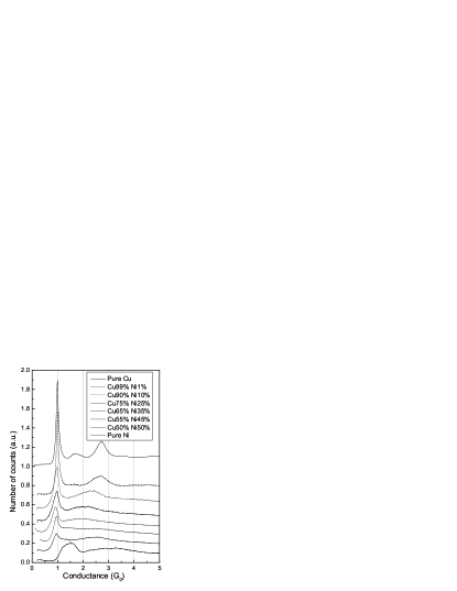
In Fig. 1, the histograms of the pure elements Cu and Ni and those of the copper alloys containing 1, 10, 25, 35, 45 and 50% nickel are presented. These measurements were done using a bias voltage of 10 mV. Topmost, the histogram of pure copper is shown. It is obtained by averaging ten histograms made on four different samples of pure copper. Three peaks can be distinguished, positioned at conductance values = 1.0 , 1.7 and 2.7 . The first peak has a higher amplitude and is sharper than the others. Close inspection makes clear that this first peak is actually slightly below 1 . At the bottom of Fig. 1, the histogram of pure nickel is shown. It is very different from the copper histogram: it exhibits a broad first peak centered around 1.6 , and a second, even broader, structure centered around 3.1 .
Looking at the histograms of the alloys, it is remarkable that for all nickel concentrations the histograms resemble the histogram of pure copper; in particular, they have a first peak a little below . Indeed, for biases lower than 200 mV and for nickel concentrations up to 50%, there is no sign of a ”nickel” peak at 1.6 . We give a possible interpretation of this effect in the next section. The second peak disappears rapidly when one increases the nickel concentration, due to shifting and broadening. With increasing nickel concentrations, three things can be seen to happen to the other peaks in the histogram: broadening, decreasing in amplitude and downshifting.
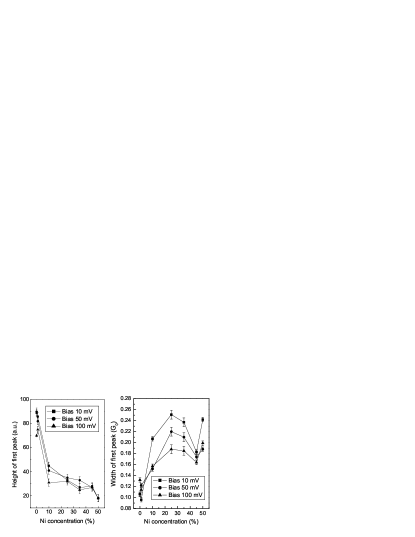
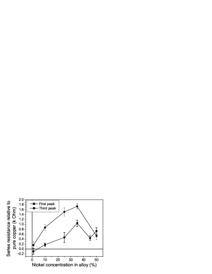
The width and height of the first peaks in the histogram are plotted in the right and left panel of Fig. 2, respectively. As can be seen, the amplitude of the peak decreases monotonously with Ni concentration. This can be explained as the result of increasing disorder. The disorder leads to slight variations in the last-plateau conductance of different scans. These variations cause the different plateaus to fall into different bins on the conductance axis, thus causing less high peaks in the histogram. The same effect gives rise to the broadening of the peaks that is observed for Ni concentrations up to 35%. Above this concentration, the width decreases to a minimum at 45%, after which it increases again. Fig. 2 also shows that the results reproduce for different biases. The main feature observed in Fig. 1 is the shift towards lower conductance values of the first and third peaks in the histogram. In Fig. 3, the series resistance corresponding to this shift is plotted as a function of the percentage of nickel in the alloy. Note that we do not calculate the shift with respect to integer multiples of , but relative to the measured positions of the corresponding peaks in the histogram of pure Cu. Results again reproduce for other biases. The shift increases roughly linearly with nickel concentration, up to 35% nickel. Two surprising features of Fig. 3 must be noted. Firstly, the series resistance is not the same for all the peaks in the histogram. Instead, the resistance corresponding to the shift of the third peak is roughly two or three times higher than the corresponding values for the first peak. The same conclusion can be reached when considering the resistance necessary to bring the first and third peaks of the pure copper histogram to the corresponding integer multiples of , namely, 60 20 and 460 respectively. This is in agreement with earlier findings PRB_Hansen97 , but contradictory to the widespread practice to bring all conductance peaks to integer multiples of by subtracting a constant series resistance. The second surprising feature of Fig. 3 is the decrease of the shift for Ni concentrations higher than 35%. This decrease corresponds to the decrease in width that was already noticed in Fig. 2. Again the minimum is at 45% Ni. We discuss a possible interpretation of this effect in the next section.
IV Discussion
The main difference between the histograms of copper and nickel, as shown in Fig. 1, is the position of the peaks. In particular, whereas copper shows a sharp first peak nearly exactly at 1 , nickel has a broad first peak centered around 1.6 . In both cases, however, it seems reasonable to assume that the first peak in the histogram corresponds to the smallest possible contact: only one atom bridging the gap between the electrodes. This is supported by the fact that the conductance invariably drops sharply to zero at the end of the plateau at 1 (Cu) or 1.6 (Ni). The difference in conductance between the different kind of atoms can be explained by taking into account their valence orbitals. As already mentioned in the introduction, copper has one spherically symmetric s valence orbital, whereas the valence orbitals of nickel are d-type. It has been shown Nature_Scheer98 that for monovalent s-type metals there is one, almost completely opened, conductance channel per atom, which gives rise to a 1-atom conductance of nearly 1 . In contrast, the five valence orbitals of a d-metal give rise to five partially opened channels, with a total conductance in the range of 1.5 - 2.5 .
We noticed that the histograms for all the alloys resemble the histogram of pure copper, in particular, the first peak is below 1 , and the third is below 2.7 . However, if we very crudely model a contact of e.g. Cu50Ni50 as consisting of two pyramids touching each other in the apexes, such that there are two constricting atoms, 25% of all contacts should end in a Cu-Cu constriction, 25% should end in a Ni-Ni constriction, and 50% should have a Cu-Ni constriction. This raises the question why we don’t see the influence of the nickel atoms in the histogram of this alloy, apart from the downshifting and smearing of its peaks. An explanation for this phenomenon might be that the Ni atoms do not take part in the forming of the contact. This might be due to surface segregation, which is known to lead to a very strong copper enrichment of the surface layers in bulk Cu-Ni PRB_Sakurai86 , due to the lower surface energy of Cu atoms. Calculations for small Cu-Ni clusters PRB_Tomanek83 show the same phenomenon: all the copper atoms present segregate to the surface of the cluster. All the atoms forming the contact in a MCBJ can be viewed as being at the ‘surface’, to the extent that their coordination number is less than in the bulk. Thus there might be a preference for Cu atoms to form the contact, which would lead to the absence of Ni peaks in the histogram of the alloy. However, this surface segregation takes places only at elevated ( 600 K) temperatures, while we performed our measurements at 4 K and at low (10 mV) bias, such that local heating of the contact is probably not sufficient for segregation to happen helko . Moreover, preliminary studies by molecular dynamics simulations jan don’t show such a segregation between Cu and Ni atoms in the contact. Possibly, however, the repeated contact indentation and breaking provides enough mobility for the atoms to obtain some degree of segregation.
Another possibility to explain the similarity between the histograms of the alloys and that of pure copper is assuming that the conductance of Cu-Ni constriction is the same as that of a Cu-Cu constriction, namely, 1 . For a contact of Cu50Ni50 in the form of two pyramids, this would lead to at least 75% of all last-atom contacts having a conductance of approximately 1 . Calculations to verify this are under way.
If the above picture is correct, adding nickel atoms indeed doesn’t change the copper histogram in a qualitative way. Instead, the nickel atoms only act as scatterers for the electrons in the banks to the contact. One would expect the amount of disorder in the banks to increase with the nickel concentration. In Fig. 3, it is shown that the series resistance increases approximately linearly with nickel concentration up to a nickel concentration of 35%. From this we conclude that it is indeed the disorder in the nanowire, in the form of impurities, that causes the downshift of the peaks in the histograms. This is in accordance with the results of the calculations cited above.
However, the sudden decrease of the series resistance when going to 45 % nickel, accompanied by a decrease of the width of the first peak, suggest that the amount of disorder decreases when one increases the nickel concentration to this value. In order to compare with the behavior of bulk copper-nickel, we have measured the bulk resistivity of the alloys at room temperature as well as at = 4.2 K. Results are presented in Fig. 4.
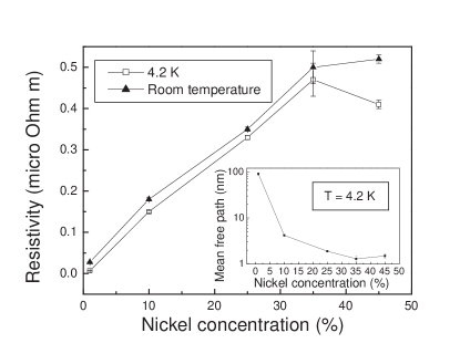
It can be seen that the low-temperature resistivity initially closely follows the RT resistivity and is linear with the nickel concentration. Upon going to 45% nickel, however, the low-temperature resistivity decreases, whereas the room temperature resistivity still increases, although less than would be expected from a linear behavior. The decrease in the shift of the peaks in the copper-nickel histograms therefore probably reflects the decrease is resistivity of bulk copper-nickel. This shows that the origin of the series resistance is probably in the banks to the contact, and is not a (quantum mechanical) effect in the contact itself. A likely explanation for the decrease is the onset of ferromagnetism in the nanowire. The ferromagnetic ordering will decrease the amount of spin-spin scattering events by decreasing the magnetic fluctuations, even though the nickel concentration increases. As a matter of fact, bulk copper-nickel becomes magnetic at 4.2 K for a nickel concentration of approximately 45% handbook . From Fig. 3 it can be seen that the resistance tends to increase again when the nickel concentration is increased to 50%, which may be explained by assuming that once the alloy is ferromagnetic, the amount of disorder in it again increases with increasing nickel concentration. The inset in Fig. 4 shows the bulk mean free paths for the electrons in several of the alloys, calculated from the resistivities using the Drude model. An important difference between the bulk material and the quantum point contacts is the behavior for low nickel concentration. It is well known that the resistivity of metals at low temperatures depends sensitively on the purity of the sample. Thus, the mean free path in pure copper at 4.2 K will be much larger than that in Cu99Ni1. On the other hand, the histograms of these two materials are nearly indistinguishable. This means that in point contacts of both materials, the mean free path is restricted by scattering from the surface and lattice defects related to the geometry of the contact, rather than by impurities. When the concentration of impurities is raised to 10%, they start to have an appreciable effect. Thus, the mean free path in the contact region of a QPC of pure copper must be in between those in bulk Cu99Ni1 and Cu90Ni10, i.e. between 5 and 30 nm. This is consistent with results obtained earlier for quantum point contacts of copper bas .
From Fig. 3 a second important feature can be inferred. It can be seen clearly that the series resistance is not the same for all the peaks in the histogram. The resistance necessary to shift the third peak in the histograms back to its value for pure copper is larger than for the first peak. The difference increases with disorder. This effect is not accounted for by any of the calculations cited above. Possibly this difference in behavior compared to the first peak can be accounted for by considering the fluctuations in Cu/Ni ratio for contacts of this size, or by a non-uniform Ni concentration due to a partial segregation of Ni atoms away from the contact area.
V Conclusion
In conclusion, we have shown, firstly, that adding nickel impurities to copper leads to an increase of the shift and smearing of the conductance peaks. This is evidence that disorder in the nanowires is a main source for the series resistance, in agreement with several theoretical papers. Up to a nickel concentration of 35%, this shift increases roughly linearly with the nickel concentration. Secondly, when the nickel percentage is increased further, the shift decreases. The latter effect may be due to a ferromagnetic transition leading to a decrease of the resistance of the mesoscopic banks. It was shown that the bulk resistivity of Cu-Ni alloys follows the same behavior as the series resistance does, which is evidence that the series resistance finds its origin in the banks to the contact rather than in the contact itself. Thirdly, we have shown that one single series resistance is not sufficient to shift all the peaks in the histogram back to the respective quantized values. Instead, it is found that the series resistance needed for the third peak is larger than that for the first. Fourthly, our measurements show that adding nickel impurities has remarkably little influence on the global shape of the copper histogram, even if the nickel concentration is raised to 50%. To explain this, we suggest that a Cu-Ni constriction has approximately the same conductance as a Cu-Cu constriction, or that there is a partial segregation of Ni atoms away from the contact.
VI Acknowledgements
This research has been supported by a Marie Curie fellowship of the European Community under contract number HPMF-CT-1999-00196. We are grateful to I.K. Yanson for fruitful discussions and to R.W.A. Hendrikx for providing the sample materials.
References
- (1) B. J. van Wees et al., Phys. Rev. Lett. 60, 848 (1988)
- (2) D. A. Wharam et al., J. Phys. C. 21 L887 (1988)
- (3) J.M. Krans et al., Phys. Rev. B 48, 14721 (1993)
- (4) J.I. Pascual et al., Phys. Rev. Lett. 71, 1852 (1993)
- (5) L. Olesen et al., Phys. Rev. Lett. 72, 2251 (1994)
- (6) See e.g. A. I. Yanson and J. M. van Ruitenbeek, Phys. Rev. Lett. 79, 2157, (1997) and refs. therein.
- (7) G. Rubio, N. Agraït and S. Vieira, Phys. Rev. Lett. 76, 2302 (1996)
- (8) T. N. Todorov and A. P. Sutton, Phys. Rev. Letters, 70, 2138 (1993)
- (9) Elke Scheer et al., Nature 394 154, (1998)
- (10) J. L. Costa-Krämer and N. García, Phys. Rev. B, 55, 12910, (1997)
- (11) K. Hansen, E. Lægsgaard, I. Stensgaard and F. Besenbacher, Phys. Rev. B, 56, 2208, (1997)
- (12) J.M. Krans et al. Nature 375, 767 (1995)
- (13) P. García-Mochales and P.A. Serena, Phys. Rev. Lett. 79, 2316, (1997)
- (14) M. Brandbyge, K. W. Jacobsen and J. K. Nørskov, Phys. Rev. B, 55, 2637, (1997)
- (15) P. García-Mochales and P.A. Serena, Phys. Rev. Lett. 79, 2316 (1997)
- (16) J. Bürki, C.A. Stafford, X. Zotos and D. Baeriswyl, Phys. Rev. B, 60, 5000 (2000)
- (17) B. Ludoph and J.M. van Ruitenbeek, Phys. Rev. B 61, 2273 (2000)
- (18) C. Z. Li, H. Sha and N. J. Tao, Phys. Rev. B 58, 6775 (1998)
- (19) See e.g. T. Sakurai et al., Phys. Rev. B 34, 8379 (1986)
- (20) D. Tománek, S. Mukherjee and K. H. Bennemann, Phys. Rev. B 28, 665 (1983)
- (21) For an estimate of the dependency of the local contact temperature on bias voltage, see H. E. van den Brom, PhD. thesis Leiden University, The Netherlands (2000)
- (22) J. W. T. Heemskerk et al., to be publised.
- (23) Y. Noat, N. D. Lang, M. van Hemert and J. M. van Ruitenbeek, to be published.
- (24) See e.g. Constitution of binary alloys, ed. M. Hansen, McGraw-Hill book company, 1953