Scanning Tunneling Microscopy of Defect States in the Semiconductor Bi2Se3
Abstract
Scanning tunneling spectroscopy images of Bi2Se3 doped with excess Bi reveal electronic defect states with a striking shape resembling clover leaves. With a simple tight-binding model we show that the geometry of the defect states in Bi2Se3 can be directly related to the position of the originating impurities. Only the Bi defects at the Se sites five atomic layers below the surface are experimentally observed. We show that this effect can be explained by the interplay of defect and surface electronic structure.
pacs:
68.35.Dv, 68.37.Ef, 73.20.Hb, 71.55.HtUnderstanding the electronic properties of defects and the ability to control them will be crucial for the performance of the future microelectronic devices kane . Scanning Tunneling Microscopy (STM) represents a unique tool for the studies of defects as it combines atomic scale resolution with local spectroscopic capability. However, STM observation and analysis of defect states in semiconductors are complicated by surface effects such as in-gap surface states and reconstruction. These effects are avoided at the (110) surfaces of a number of III-V semiconducting systems gaasbands , attracting extensive research sigaas –charge . A number of point defect types have been observed. However, positions of these defects with respect to the surface plane could be inferred only from indirect observations. The interpretation of such observations is complicated by the drastic effect the surface proximity may have on the defect states el2 .
Modeling STM measurements of defects in semiconductors is not straightforward: Approximation of the STM images by maps of the local surface electronic density of states tersoff is justified only if the charge relaxation rates of defect states significantly exceed the tunneling rate of electrons between the tip and the sample theory . Tip-induced effects also need to be taken into account. These may include both local band bending sigaas , and charging of the defect states by the tunneling current, resulting in bias voltage-dependant lattice relaxation in the vicinity of the defect atoms charge . Careful analysis is necessary to clearly separate these effects from the intrinsic defect properties, and the bulk features of the observed defect states from the surface effects.
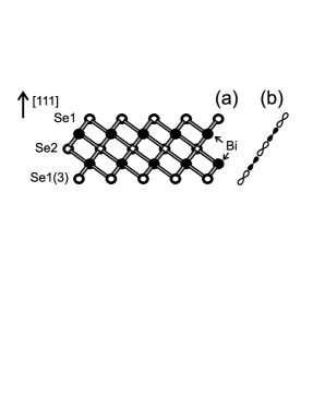
In this paper we present cryogenic STM and scanning tunneling spectroscopy (STS) studies of the layered narrow gap semiconductor Bi2Se3, which can be viewed as a model system for the STM study of near-surface defect states. The bonding scheme of Bi2Se3 allows a direct determination of the position of a subsurface defect atom with respect to the surface: Atomic planes consisting of either Bi or Se hexagonally arranged atoms are stacked in a close-packing fcc fashion; 5 atomic planes with atomic order Se1-Bi-Se2-Bi-Se1 (Fig. 1(a)) form a layer. The layers are weakly bound to each other by Se1-Se1 bonds. Both valence and conduction bands are formed almost exclusively by the and orbitals of Se and Bi respectively bisebands . For each atom, the closest neighbors from the adjacent atomic planes form almost a regular octahedron, so the bonding can be roughly approximated by strongly interacting chains of atomic -orbitals (Fig. 1(b)), with a weaker -type interaction between adjacent chains. A substitutional defect is therefore likely to produce a perturbation in the electronic local density of states (DOS) predominantly along the three chains passing through the defect atom. Hence, the defect state should be observed at the surface as three spots of modified DOS around the atoms terminating these chains at the surface.
We have performed STM and STS measurements using a custom built low-temperature microscope with direct immersion in liquid He-4 tessmer . Stoichiometric Bi2Se3 single crystal samples, as well samples doped with 2–5% excess Bi or Se were grown by a directional solidification technique. The stoichiometric as-grown Bi2Se3 samples are n-type with carrier concentration of about 1019 cm-3. Doping samples with excess Bi introduces substitutional Bi defects at the Se sites (BiSe antisites), which are shallow acceptors. However, because of the low solubility of Bi in Bi2Se3 lovett , the Bi-doped samples are n-type due to the compensating defects. Doping samples with excess Se introduces shallow donor-type Se substitutional defects at the Bi sites (SeBi antisites). The samples are sufficiently inert to obtain atomic resolution in air. However, to minimize the surface contamination, in the experiments reported here, the samples were cleaved in situ or in a glove box directly attached to the STM setup in ultrapure He gas prior to transfer to the STM with subsequent cooling to T=4.2 K.
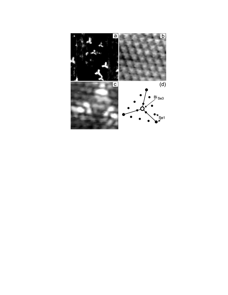
To map out the defect states, we have performed differential current imaging tunneling spectroscopy (CITS) measurements strosciobook . The CITS maps were acquired by fixing the tip at each point during topographic imaging and measuring the differential conductance at various bias voltages with the feedback loop disabled. Only Bi-doped samples exhibited an appreciable density of observable defect states, as shown in Fig. 2(a) for a sample doped with 5% excess Bi (Bi2Se2.85). The map was acquired with sample bias Vb= V in the feedback mode (with tunneling current set to pA), and Vb= V for the conductivity measurement. The defects appear as regular clover-shaped bright features, indicating areas with locally enhanced conductance at Vb= V. Irregular spots in this image (mostly in the upper left corner) resulted from topographic defects. The data discussed below were obtained on a more weakly doped Bi2Se2.95 sample, where the defect density was reduced.
Fig. 2(b),(c) present topographic maps of the sample area encompassing an isolated clover-shaped defect state. Topographic image Fig. 2(b), acquired at a sample bias voltage Vb= V, shows a periodic atomic structure, indicating no significant structural variation associated with the defect. The height of the atomic corrugations in Fig. 2(b) is about pm. Fig. 2(c) shows a topographic image of the same area acquired at Vb= V, where the largest corrugations, locally enhanced by tunneling through the defect state, are about pm high. The highest amplitude of the defect state correlates with positions of three surface Se atoms (marked with larger black circles in schematic Fig. 2(d)), forming a regular triangle. These atoms terminate three -bonded chains passing through the Se1 site five atomic layers below the surface, for which we also use notation Se3. Since the observed defects appear only in Bi-doped samples and they originate from Se sites, we attribute them to the BiSe3 antisites.
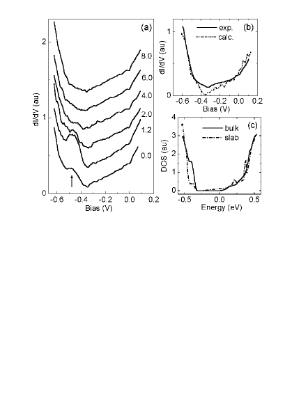
Fig. 3(a) presents a series of differential conductance spectra acquired in the vicinity of an isolated defect. The spectra were obtained by numerical differentiation of 60 I-V curves with setpoint parameters Vb= V, I= nA. At the measurement temperature of 4.2 K, thermal broadening is negligible on the displayed bias voltage scale. The defect state appears as a broad resonance (indicated by an arrow) in the energy range where the differential conductance is suppressed away from the defect. The established semiconducting gap value is about eV bisebands , lovett , therefore the defect levels appear inside the valence band. Theoretical modeling is necessary to understand this spectroscopic feature, as well as why only BiSe antisites five atomic planes below the surface are observed.
First, we performed ab initio calculations in the full potential relativistic LAPW formalism lapw within LDA approximation. To model the surface, a supercell geometry was used, with distance between slabs (consisting of 15 atomic planes, or 3 layers, each) increased by to nm as compared to the bulk crystal structure. The calculated band structure did not exhibit significant variation for the slab separation larger than – nm, therefore we found the slab separation of nm, used for the calculations presented below, sufficient for modeling the surface. The differential conductance spectra were approximated by the local DOS in the center of the gap between the slabs tersoff . The calculation presented in Fig. 3(b) was performed for a position above a Se1 atom, although we found the variation of the calculated spectra with position respective to the surface atoms to be insignificant. The calculation reproduces both the finite conductance in the bulk semiconducting gap, and the suppressed conductance just below the gap. In Fig. 3(c), the total DOS calculated in the slab geometry is compared to the calculation of the bulk DOS, which reproduces the accepted semiconducting gap value of eV LDAcomment . Band structure analysis indicates that the highest valence band (HVB) states are predominantly Se1-Se1 antibonding type. As the Se1-Se1 bonds are broken at the surface, the splitting of these states is reduced, resulting in the observed suppression of the differential conductance in the HVB energy range (Fig. 3(b)). The states that appear in the gap have high dispersion along the surface. They originate from the rehybridization of the surface Se1 valence with Bi conduction states, bringing the latter down below the bulk conduction band minimum.
ab initio calculations of a single defect state are complicated by the large cluster or supercell size necessary to model the impurity states without introducing artificial interaction between defects. Instead we use a LCAO approximation as a simple model of the system bisebands . This model presents just a qualitative argument and is not capable of reproducing the detailed electronic structure or the semiconducting gap value. However, it gives a surprisingly good qualitative agreement with the experimental observations and first principles calculations. In a tight binding formalism
| (1) |
where are atomic wave functions and are off-diagonal matrix elements of . We approximate by the atomic term values harrison of Bi and Se, and take into account only interaction between the closest neighbors, as shown in Fig. 1(b). Thus the problem is reduced to a system of noninteracting one-dimensional chains, with three matrix elements ,, and , corresponding to Se1-Bi, Se2-Bi, and Se1-Se1 bonds. Consider first a 5-atom chain Se1-Bi-Se2-Bi-Se3 (we also call it a unit), representing a single layer in our approximation. Here Se3 position is equivalent to Se1. The highest energy filled state is nonbonding
| (2) |
We model the bulk by a long chain of Se1-Bi-Se2-Bi-Se1 units, with the interaction between layers expressed by . Due to the Se1-Se1 interaction, the nonbonding level is split, and the HVB states become antibonding in the sense of Se1-Se1 bond character. The splitting is large, because the state Eq.(2) has a significant weight on the interlayer Se1 atoms. As the interlayer bonds are broken at the surface, the HVB states of a chain decay at the surface (the end of the chain), as shown in Fig. 4(a), where the antibonding character of the valence band maximum (VBM) state can also be seen. In semiclassical terms, as illustrated in Fig. 4(b), the surface gap is larger than the bulk value. This effect is in agreement with the more accurate first principles calculations and spectroscopic measurements, Fig. 3(b), (c).
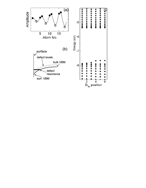
To highlight the importance of these surface effects for the observation of the defect states, in Fig. 4(c) we plot the calculated dependence of the near-gap energy levels on the position of the BiSe antisite. The second layer (positions 4–6) is only weakly affected by the proximity of the surface, so the defect level is split from the VBM and its energy is only weakly dependant on the position. As the antisite position approaches the surface (positions 1–3), the defect level energy is reduced as the surface gap opens up, so that the defect state merges with the bulk valence states, forming a resonance inside the bulk valence band. This behavior is supported by the semiclassical picture shown in Fig. 4(b). Only the BiSe3 state is observed in the experiment, because, as our model suggests, BiSe1 and BiSe2 states are so much lowered in energy by the proximity of the surface that they form small amplitude broad resonances in the valence band. STM images do not exhibit defect features associated with BiSe antisite in the second layer. Our model suggests, that they form bound states in the bulk gap, which cannot sustain STM current. Surface effects thus provide a mechanism for the charge relaxation of near-surface defect states through the bulk valence band.
Similar surface effects should be observable in other semiconductors, e.g. at (110) surface of GaAs, where the valence band is, like in Bi2Se3, suppressed at the surface gaasbands . As a result, in-gap impurity states may become resonances in the valence band, if the originating impurities are sufficiently close to the surface el2 . This suggests an alternative explanation for some of the published results sigaas2 . It may also be possible to induce the resonant behavior of near-surface defects by careful control of the surface band bending with doping and/or external field.
Resonances induced by near-surface defects can be contrasted to the bulk-like in-gap states. The origin of the spectroscopic broadening of the latter feenstra , and the mechanisms of their charge relaxation, allowing their observation with STM, need further theoretical and experimental studies theory . Variable temperature studies of the influence of the local defect distribution on the spectroscopic features of defect states may provide insight into these issues, and Bi2Se3 represents a convenient model system for such studies.
In summary, we have observed clover-shaped defect states in Bi2Se3 doped with excess Bi, which appear as resonances in the high valence band, and can be attributed to BiSe antisites in fifth atomic layer from the surface. In the analysis of these defect states, we have demonstrated the importance of the surface effects for the electronic structure of near-surface defects. While BiSe defects in the bulk Bi2Se3 form shallow acceptor levels, the near-surface defects produce resonances in the energy range of the bulk valence states, which are suppressed at the surface. We suggest that similar surface effects are likely to be observable in other semiconducting systems.
We thank J. Nogami, Norman O. Birge, M. I. Dykman, T. Hogan, and S. Lal for helpful discussions. This work was supported in part by NSF (DMR-0075230) and ONR/DARPA (N00014-01-1-0728). SHT acknowledges support of the Alfred P. Sloan Foundation.
References
- (1) See, e.g. B. E. Kane, Nature 393, 133 (1998).
- (2) Xuejun Zhu et al., Phys. Rev. Lett. 63, 2112 (1989).
- (3) J. F. Zheng et al., Phys. Rev. Lett. 72, 1490 (1994).
- (4) R. M. Feenstra, J. M. Woodall, and G. D. Pettit, Phys. Rev. Lett. 71, 1176 (1993).
- (5) B. Grandidier et al, Appl. Phys. Lett. 72, 2454 (1998).
- (6) Chr. Wittneven it et al., Phys. Rev. Lett. 81, 5616 (1998).
- (7) B. Grandidier et al., Appl. Phys. Lett. 74, 1439 (1999).
- (8) Ph. Ebert, K. Urban, and M. G. Lagally, Phys. Rev. Lett. 72, 840 (1994).
- (9) R. B. Capaz, K. Cho, and J. D. Joannopoulos, Phys. Rev. Lett 75, 1811 (1995).
- (10) J. Tersoff and D. R. Hamann, Phys. Rev. Lett. 50, 1998 (1983).
- (11) X. de la Broise et al., Phys. Rev. B 61, 2138 (2000).
- (12) S. K. Mishra, S. Satpathy, and O. Jepsen, J. Phys.: Cond. Matt. 9, 461 (1997).
- (13) S. H. Tessmer, D. J. Van Harlingen, and J. W. Lyding, Rev. Sci. Instrum. 65, 2855 (1994).
- (14) D. R. Lovett, Semimetals and Narrow-Bandgap Semiconductors (Pion Limited, London, UK, 1977).
- (15) J. A. Stroscio and R. M. Feenstra, in Scanning Tunneling Microscopy, Methods in Experimental Physics Vol. 27 (Academic Press, New York, 1993).
- (16) David J. Singh, Plane waves, Pseudopotentials and the LAPW method, (Kluwer Academic Publishers, Boston, 1994).
- (17) Although LDA approximation usually underestimates the semiconducting gap value, it has been rather successful in application to chalcogenide semiconductors. See, e.g. P. Larson, S. D. Mahanti, and M. G. Kanatzidis, Phys. Rev. B 61, 8162 (2000).
- (18) W. A. Harrison, Electronic Structure and the Properties of Solids (W. H. Freeman and Co., San Francisco, 1980).