Single electron transistors with high quality superconducting niobium islands
Abstract
Deep submicron Al/AlOx/Nb tunnel junctions and single electron transistors with niobium islands were fabricated by electron beam gun shadow evaporation. Using stencil masks consisting of the thermostable polymer polyethersulfone (PES) and germanium, high quality niobium patterns with good superconducting properties and a gap energy of up to meV were achieved. The characteristics of the transistors show special features due to tunneling of single Cooper pairs and significant gate modulation in both the superconducting and the normal state.
pacs:
73.23.Hk, 74.76.-w, 81.15.-z, 85.40.UxSuperconducting quantum coherent devices with small tunnel junctions offer the possibility of manipulating single Cooper pairs and may be used to construct current standards Likharev85 and charge qubits Makhlin01 . For optimum performance, many devices require that the Josephson coupling energy is of the same order as the charging energy , where k, is the junction tunnel resistance, the superconducting gap energy, and the total capacitance of the island. With modern nanotechniques it is possible to reduce and hence to increase in Al based junctions ( meV), but it is hard to keep because this would require very transparent barriers. With the use of Nb based junctions ( meV) it should be possible to increase the Josephson coupling energy by almost one order of magnitude for the same tunnel resistance. Further, an increased is important since it should suppress disturbing quasiparticle tunneling onto/from the island Tuominen92 . Al-Nb junctions are a first step in this direction because . These relations follow from the equation for the Josephson coupling energy in junctions with different electrode materials A and B for (see, e.g., Barone82 ):
Here, is the complete elliptic integral of the first kind.
It has been shown that rather small Nb based junctions (areas about 0.1 m2) with high quality characteristics can be fabricated from Nb/AlOx/Nb trilayers by etching and planarization techniques Pavolotsky99 , but single charge devices prepared with these junctions still suffer from high capacitances ( fF).
Shadow or angle evaporation through a suspended mask is a common technique for the fabrication of ultrasmall tunnel junctions with low capacitance Niem-Dolan . Usually, polymethylmethacrylate (PMMA) and related copolymers (PMMA-MAA) are used to create high resolution suspended stencil masks by electron beam lithography. These masks provide easy lift-off and are successfully used for the preparation of devices based on soft materials such as aluminum Geerligs90 . Unfortunately, for the fabrication of submicron Nb structures, the use of PMMA entails strong deterioration of the superconducting properties Harada94 ; Hoss99 ; Dubos00 . The most important reason for this is the outgassing of the PMMA polymer during the evaporation of the high-melting Nb due to radiation heating from the evaporation source Hoss99 ; Dubos00 . For high-melting materials nonorganic evaporation masks were developed, made of two metallic Howard78 ; Zant90 or two dielectric layers Hoss99 . However, the metallic masks pose problems in the fabrication of deep submicron structures because of their rough edges, and dielectric masks cannot be lifted off after evaporation. Dubos et al. developed a novel lift-off process for the preparation of high quality submicron Nb structures, based on the use of the thermostable polymer polyethersulfone (PES) Dubos00 . PES remains mechanically tough up to temperatures of about 200 ∘C and shows very low outgassing compared to PMMA.
In this paper, we present for the first time results on high quality superconducting Al/AlOx/Nb tunnel junction samples fabricated using PES based stencil masks. In the first step, the PES layer (Ultrason E6020P made by BASF, dissolved in N-methylpyrrolidone (NMP)) was spun onto thermally oxidized three-inch Si wafers and baked for 20 minutes at 230 ∘C to form the bottom layer 420 nm in thickness. Next, a 35 nm thick Ge layer was thermally evaporated onto the PES layer. Finally, a PMMA layer 130 nm thick was spun on top of the germanium. This layer was patterned by electron beam lithography and served as a mask for reactive ion etching of the Ge layer in a CF4 plasma. An undercut of approximately 300 nm in the PES layer was created by oxygen plasma etching. In this etching step, the PMMA top layer was completely removed, the final stencil mask was composed of a PES bottom layer and a Ge top layer formed the suspended bridges. The samples were fabricated by two-angle E-gun evaporation in an ultrahigh vacuum system with a base pressure of about mbar onto a substrate wafer thermally anchored to a copper block at room temperature. The sample was tilted to a first angle and an Al layer 35 nm in thickness was evaporated. Next, the AlOx tunnel barrier was formed by oxidation in pure O2. Process time and pressure were varied for different wafers. After pumping down of the O2, an Nb layer 40 nm thick was evaporated using a second tilt angle. Finally, the stencil mask was lifted off in NMP.
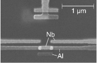
We prepared single junctions and single electron transistors that allowed four terminal measurements to be made. The transistors consisted of Al wires, an Nb island and an Al/Nb gate electrode (Fig. 1). Several devices of varying junction size were included on every wafer, and the maximum nominal junction size was about 100 nm 100 nm. Experiments were carried out in a dilution refrigerator at a base temperature of mK. Electrical biasing and signal amplification were performed using symmetrical current (or voltage) bias and low-noise preamplifiers with all signal lines RF filtered by Thermocoax cable pieces 1 m long. We investigated samples from two wafers prepared under different barrier oxidation conditions and found a yield of the working structures of about 80 %. The sample layouts on the two wafers were similar except for the length of the island which led to different gate capacitance values.
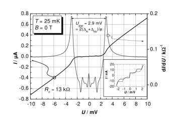
On the first wafer (heavier oxidation), we found transistor samples with gap voltages between 2.5 and 2.65 mV according to the maxima of the differential conductivity plots in the superconducting state ( T). Total resistances from 70 to 250 k were derived from the -curves when the samples were driven to the normal state ( T), and the values for the total island capacitance were - 0.6 fF. On the second wafer (lighter oxidation), we had single Al/AlOx/Nb junctions ( meV, - 45 k) and transistors with - 2.9 mV, - 70 k, - 0.6 fF. The achieved in our Al/Nb transistors thus was of the order of the island capacitance for typical Al devices Geerligs90 ; Tuominen92 . Switching currents up to some nA were measured on samples of the second wafer (inset in Fig. 2) Footnote . The ratios of the transistors were estimated to be in the range of 0.03 - 0.3 for the first and of 0.16 - 1.2 for the second wafer.
The gap voltages observed are significantly higher compared with recent results reported for similar Al/AlOx/Nb transistors Harada94 ; Born01 . From the maximum gap voltages of about 2.9 mV observed for single junctions and transistors on the second wafer, we find that meV (Fig. 2). Assuming that meV Tuominen92 ; Harada94 ; Born01 ; JQP , we derive the gap energy of the Nb islands to be about 1.25 meV. Preliminary measurements showed that signatures of superconductivity persist up to temperatures of about - 8 K, which we identify with the critical temperature of the Nb islands (cf. K for bulk Nb). According to the formula from BCS theory, this agrees well with the values for derived from the gap voltage.
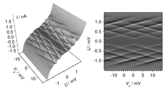
Significant current peaks appeared in the subgap voltage range of the transistors’ curves, especially marked in samples on the wafer with the more heavily oxidized barrier where the ratios were only 0.03 - 0.3. These features, showing up as rhombic structures in the - plane (Fig. 3), are attributed to different resonant tunneling processes involving combined single Cooper pair and quasiparticle tunneling, known as “Josephson quasiparticle” cycles JQP . The current peaks could be modulated by the gate voltage with a period corresponding to . They disappeared when a magnetic field of T was applied, sufficient to suppress the superconductivity in the Al electrodes. This supports that the current peaks were linked with the superconductivity of the two electrodes. An influence of the magnetic field upon the shapes of the curves was observed up to T, indicating the persistence of superconducting domains in the Nb film island.
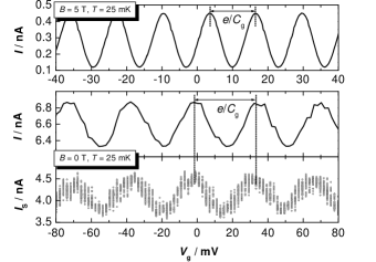
Besides the gate modulation in the normal state, we also investigated the variation of the switching currents with on the transistors with measurable critical currents (Fig. 4). Measurements of were performed using a sample-and-hold technique while the sample was biased with a sawtooth-shaped signal at frequencies Hz. In all samples we found that was modulated -periodically. Together with the leakage currents observed in the subgap regions of the single junctions, this suggests the presence of quasiparticles that might enter the Nb island via parasitic conductance channels, or the presence of intra-gap energy states caused by impurities and allowing quasiparticle tunneling at low bias.
In summary, we have fabricated Al/AlOx/Nb single electron tunnel devices by shadow evaporation using a PES based trilayer mask. This method allows the junction dimensions to be further reduced. The superconducting Nb islands are characterized by a gap energy of up to meV close to the bulk value. Unexpectedly, all gate modulation characteristics measured on the single electron transistors showed a periodicity corresponding to , so that further investigations are called for. The ratio of characteristic energies in these samples varies over a wide range, clearing the way for devices operating on single pairs. Our results are a first step towards the highly desirable Nb/AlOx/Nb junctions for future mesoscopic devices.
The authors wish to thank BASF for providing a sample of PES, and P. Ågren for discussions about the sample-and-hold measurement technique.
References
- (1) K. K. Likharev and A. B. Zorin, J. Low Temp. Phys. 59, 347 (1985).
- (2) Yu. Makhlin, G. Schön, and A. Shnirman, Rev. Mod. Phys. 73, 357 (2001).
- (3) M. T. Tuominen, J. M. Hergenrother, T. S. Tighe, and M. Tinkham, Phys. Rev. Lett. 69, 1997 (1992).
- (4) A. Barone and G. Paterno, Physics and applications of the Josephson effect, John Wiley & Sons, New York (1982).
- (5) A. B. Pavolotsky, T. Weimann, H. Scherer, V. A. Krupenin, J. Niemeyer, and A. B. Zorin, J. Vac. Sci. Technol. B 17, 230 (1999).
- (6) J. Niemeyer, PTB-Mitt. 84, 251 (1974); G. J. Dolan, Appl. Phys. Lett. 31, 337 (1977).
- (7) L. J. Geerligs, Classical and quantum charge dynamics in small tunnel junctions, thesis, Delft University of Technology (1990).
- (8) Y. Harada, D. B. Haviland, P. Delsing, C. D. Chen, and T. Claeson, Appl. Phys. Lett. 65, 636 (1994).
- (9) T. Hoss, C. Strunk and C. Schönenberger, Microelectron. Eng. 46, 149 (1999).
- (10) P. Dubos, P. Charlat, Th. Crozes, P. Paniez, and P. Pannetier, J. Vac. Sci. Technol. B 18, 122 (2000).
- (11) R. E. Howard, Appl. Phys. Lett. 33, 1034 (1978).
- (12) H. S. J. van der Zant, H. A. Rijken, and J. E. Mooij, J. Low Temp. Phys. 79, 289 (1990).
- (13) For this work we did not modify the environmental impedance to achieve large switching current values; cf. D. Vion, M. Götz, P. Joyez, D. Esteve, and M. Devoret, Phys. Rev. Lett. 77, 3435 (1996).
- (14) D. Born, T. Wagner, W. Krech, U. Hübner, and L. Fritzsch, IEEE Trans. Appl. Supercond. 11, 373 (2001).
- (15) T. A. Fulton et al., Phys. Rev. Lett 63, 1307 (1989); A. Maassen van den Brink et al., Phys. Rev. Lett. 67, 3030 (1991); Y. Nakamura et al., Jpn. J. Appl. Phys. 34, 4562 (1995).