Spin injection and spin accumulation in permalloy-copper mesoscopic spin valves.
Abstract
We study the electrical injection and detection of spin currents in a lateral spin valve device, using permalloy (Py) as ferromagnetic injecting and detecting electrodes and copper (Cu) as non-magnetic metal. Our multi-terminal geometry allows us to experimentally distinguish different magneto resistance signals, being 1) the spin valve effect, 2) the anomalous magneto resistance (AMR) effect and 3) Hall effects. We find that the AMR contribution of the Py contacts can be much bigger than the amplitude of the spin valve effect, making it impossible to observe the spin valve effect in a ’conventional’ measurement geometry. However, these ’contact’ magneto resistance signals can be used to monitor the magnetization reversal process, making it possible to determine the magnetic switching fields of the Py contacts of the spin valve device. In a ’non local’ spin valve measurement we are able to completely isolate the spin valve signal and observe clear spin accumulation signals at K as well as at room temperature. We obtain spin diffusion lengths in copper of micrometer and nm at K and room temperature respectively.
I introduction
Spintronics is a rapidly emerging field in which one tries to study or make explicit use of the spin degree of freedom of the electron. Sofar, the most well known examples of spintronics are the tunneling magneto resistance (TMR) of magnetic tunnel junctions, and the giant magneto resistance (GMR) of multilayers[1, 2, 3]. A new direction is emerging, where one actually wants to inject spin currents, transfer and manipulate the spin information, and detect the resulting spin polarization. Because of spin-orbit interaction, the electron spin can be flipped and consequently a spin polarized current will have a finite lifetime. For this reason it is necessary to study spin transport in systems, where the ’time of flight’ of the electrons between the injector and detector is shorter than the spin flip time. In diffusive metallic systems, this corresponds to typical length scales of a micrometer. We use a lateral mesosopic spin valve, to access and probe this length scale[4]. It consists of a ferromagnetic injector electrode and detector electrode, separated over a distance by a normal metal region, see Fig. 2.
In this paper a review of the basic model for spin transport in the diffusive transport regime will be given and applied to our multi-terminal device geometry. Secondly, a description and measurements of the magnetic switching behavior of the Py electrodes used in the spin valve device will be presented. Finally measurements of the spin valve effect in a ’conventional’ and ’non-local’ geometry will be shown and analyzed using the model for spin transport in the diffusive regime.
II Theory of spin injection and accumulation
We focus on the diffusive transport regime, which applies when the mean free path is shorter than the device dimensions. The description of electrical transport in a ferromagnet in terms of a two-current (spin-up and spin-down) model dates back to Fert and Campbell [5]. Van Son et al. [6] have extended the model to describe transport through ferromagnet-normal metal interfaces. A firm theoretical underpinning, based on a Boltzmann transport equation has been given by Valet and Fert [7]. They have applied the model to describe the effects of spin accumulation and spin dependent scattering on the giant magneto resistance (GMR) effect in magnetic multilayers. This ”standard” model allows for a detailed quantitative analysis of the experimental results.
An alternative model, based on thermodynamic considerations, has been put forward and applied by Johnson [8]. In principle both models describe the same physics, and should therefore be equivalent. However, the Johnson model has a drawback in that it does not allow a direct calculation of the spin polarization of the current ( in refs.VII and VII), whereas in the standard model all measurable quantities can be directly related to the parameters of the experimental system.
The transport in a ferromagnet is described by spin dependent conductivities:
| (1) | |||||
| (2) |
where denotes the spin dependent density of states (DOS) at the Fermi energy, and the spin dependent diffusion constants, expressed in the spin dependent Fermi velocities , and electron mean free paths . Note that the spin dependence of the conductivities is determined by both density of states and diffusion constants. This should be contrasted with magnetic F/I/F or F/I/N tunnel junctions, where the spin polarization of the tunneling electrons is determined by the spin-dependent DOS. Also in a typical ferromagnet several bands (which generally have different spin dependent density of states) contribute to the transport. However, provided that the elastic scattering time and the interband scattering times are shorter than the spin flip times (which is usually the case) the transport can still be described in terms of well defined spin up and spin down conductivities.
Because the spin up and spin down conductivities are different, the current in the bulk ferromagnet will be distributed accordingly over the two spin channels:
| (3) | |||||
| (4) |
where are the spin up and spin down current densities and is the absolute value of the electronic charge. According to eqs. 3 and 4 the current flowing in a bulk ferromagnet is spin polarized, with a polarization given by:
| (5) |
The next step is the introduction of spin flip processes, described by a spin flip time for the average time to flip an up-spin to a down-spin, and for the reverse process. The detailed balance principle imposes that , so that in equilibrium no net spin scattering takes place. As pointed out already, usually these spin-flip times are larger than the momentum scattering time . The transport can then be described in terms of the parallel diffusion of the two spin species, where the densities are controlled by spin-flip processes. It should be noted however that in particular in ferromagnets (e.g. permalloy[10]) the spin flip times may become comparable to the momentum scattering time. In this case an (additional) spin-mixing resistance arises [2], which we will not discuss further here.
The effect of the spin-flip processes can now be described by the following equation (assuming diffusion in one dimension only):
| (6) |
where is the spin averaged diffusion constant, and the spin-relaxation time is given by: . Using the requirement of current conservation, the general solution of eq. 6 for a uniform ferromagnet or non-magnetic wire is now given by:
| (7) | |||||
| (8) |
where we have introduced the spin flip diffusion length . The coefficients A,B,C, and D are determined by the boundary conditions imposed at the junctions where the wires is coupled to other wires. In the absence of spin flip scattering at the interfaces the boundary conditions are: 1) continuity of , at the interface, and 2) conservation of spin-up and spin-down currents , across the interface.
III Spin accumulation in multi-terminal spin valve structures
We will now apply the ”standard” model of spin injection to a multi-terminal geometry, which reflects our device geometry used in the experiment, see Fig.1a.
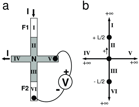
In our (1-dimensional) geometry we can identify 6 different regions for which eqs. 7 and 8 have to be solved according to their boundary conditions at the interface. The geometry is schematically shown in Fig.1b, where the 6 different regions are marked with roman letters I to VI. According to eq. 7 the equations for the spin up electrochemical potentials in these regions, assuming parallel magnetization of the ferromagnetic regions, read:
| () | ||||
| () | ||||
| () | ||||
| () | ||||
| () | ||||
| () |
where we have written and and are 9 unknown constants. The equations for the spin down electrochemical potential in the six regions of fig. 1 can be found by putting a minus sign in front of the constants and in eqs. to . Constant is the most valuable to extract from this set of equations, for it gives the difference between the voltage measured with a normal metal probe at the center of the normal metal cross in fig. 1a and a ferromagnetic voltage probe. Solving the eqs. to by taking the continuity of the spin up and spin down electrochemical potentials and the conservation of spin up and spin down currents at the 3 nodes of Fig. 1b, one obtains:
| (9) |
where .
In the situation where the ferromagnets have an anti-parallel magnetization alignment, the constant of eq. 9 gets a minus sign in front . Upon changing from parallel to anti-parallel magnetization configuration (a spin valve measurement) a difference of will be detected in electrochemical potential between a normal metal and ferromagnetic voltage probe. This leads to the definition of the so-called spin-coupled or spin-dependent resistance of :
| (10) |
Equation 10 shows that for , the magnitude of the spin signal will decay exponentially as a function of L. In the opposite limit, , the spin signal has a 1/L dependence:
| (11) |
Actually, for eq. 11 to hold a more precise constraint has to be full filled, requiring the relation to be satisfied. However, the important point to notice is that eq. 11 clearly shows that even in the situation when there are no spin flip processes in the normal metal (), the spin signal is reduced with increasing . The reason is that the spin dependent resistance of the injecting and detecting ferromagnets remains constant for the two spin channels, whereas the spin independent resistance of the normal metal increases linearly with L.
Finally, the current polarization at the interface of the current injecting contact, defined as , can be calculated. For parallel magnetized ferromagnetic electrodes the polarization P yields:
| (12) |
| (13) |
IV sample fabrication
We use permalloy (Py) electrodes to drive a spin polarized current into copper (Cu) crossed strips, see fig. 2.
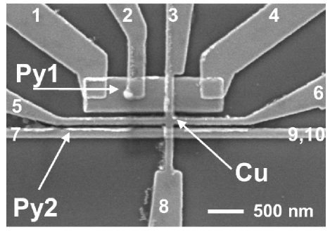
The devices are fabricated in two steps on a thermally oxidized Si wafer by means of conventional e-beam lithography with PMMA resist. To avoid magnetic fringe fields from the ferromagnetic electrodes, the nm thick Py electrodes were sputter deposited first on a thermally oxidized silicon substrate, using a nm tantalum (Ta) adhesion layer and applying a small B-field of mT along the long axis of the Py electrodes. In the second fabrication step, 50 nm thick crossed Cu strips were deposited by e-gun evaporation in a mbar vacuum. Prior to the Cu deposition, around nm of Py material was removed of the Py electrodes by ion milling, thereby removing the oxide to ensure transparent contacts. The conductivities of the Py and Cu films were determined to be and at RT. At 4.2 K both conductivities increased by a factor 2.
V Magnetic switching of the Py electrodes
The resistance of a single ferromagnetic strip is a few percent smaller when the magnetization direction is perpendicular to the current direction as compared to a parallel alignment. This effect is known as the anomalous magneto resistance(AMR) effect[12]. The AMR effect can therefore be used to monitor the magnetization reversal or ’switching’ behavior of the ferromagnetic Py electrodes[13]. Different models can be considered for describing the magnetization reversal processes in mesoscopic wires[14].
A Magnetization reversal models
The simplest description is provided by the Stoner and Wohlfarth model (SW)[15]. It assumes a single ferromagnetic domain and coherent magnetization rotation. Neglecting the magneto-crystalline anisotropy, the total energy for an ellipsoid of revolution is written as a sum of magnetostatic and shape anisotropy energies:
| (14) |
where is the saturation magnetization, and are the demagnetization factors, and and are the angles between the magnetization direction and the applied field, and, respectively, the external field and the easy axis. The first term on the right of eq. 14 represents the shape anistropy energy of the ellipsoid, which is equal to the magnetostatic self-energy of the particle. For an elongated ellipsoid along the z-axis the demagnetization factors would be and . The angle between the magnetization and the applied field for a given field can be determined analytically by minimizing the total energy. The switching or coercive field as a function of the direction of the applied field reads:
| (15) |
where is the saturation field in perpendicular direction, which corresponds to the demagnetization field along the (short) x-axis of the ellipsoid of revolution. We thus obtain an upper value estimate of the switching field for a permalloy ellipsoid of: , using .
However for fields applied parallel to the easy axis (small ) of a mesoscopic wire, it was found that the switching field is one order of magnitude smaller than the SW-model predicts[16, 17, 18, 19, 20, 21]. To explain these low switching fields two other switching mechanisms have been proposed: a magnetization curling process and a domain-wall nucleation process.
The curling model assumes that the magnetization direction rotates in a plane perpendicular to the anisotropy axis of the wire, effectively reducing the longitudinal component of the magnetization and hence the magnitude of the switching field[22, 23, 24]. For rectangular shaped strips, the upper and lower bound of the magnitude of the switching field have been calculated for a B-field applied parallel to the easy axis () of the strip. For aspect ratios , where is width and is the height of the strip, these upper and lower bounds are the same. The magnitude of switching field for a magnetic field applied parallel to the easy axis (), as calculated by Aharoni, can then be written as[23]:
| (16) |
where is the exchange length, being the exchange constant and is the saturation magnetization. For permalloy we find that , using and . For a nm wide rectangular Py electrode and a field applied parallel to the long (easy) axis, we would thus obtain a switching field of mT.
The other mechanism assumes that the switching of the magnetization is mediated by the nucleation of a domain-wall [25, 26]. A domain-wall is nucleated (annihilated) when the cost of exchange energy associated with the domain wall is lower (higher) than the gain in magnetostatic energy upon increasing the external field. Once it is nucleated it sweeps through the material, thereby lowering the total magneto static energy. This mechanism has been confirmed experimentally by Lorentz micrography by Otani[27]. Recent MFM studies of wide iron and permalloy wires seem to indicate that in these wires a multi-domain structure is formed during the reversal process[28, 29]. However an analytical expression of the magnitude of the nucleation field cannot easily be given, as one has to numerically solve the time dependent Landau-Lifschitz equations for each value of the applied magnetic field.
B The AMR behavior of rectangular Py electrodes
The AMR behavior of the , and nm wide rectangular Py electrodes used in the spin valve samples, as shown in fig. 2, was measured four terminal by using contacts and as current contacts and and as voltage contacts. In fig. 3 the magneto resistance behavior at K of the (bottom curves) and (top curves) sized Py electrodes is shown, where the magnetic field is applied parallel to the long axis of the Py electrode ().
Coming from a negative B-field the electrode already has a change in the resistance before the magnetic field reaches zero. After this first drop in the resistance at mT, a broad step like transition range is observed up to mT, which indicates that the Py strip breaks up in a multiple domain structure. The amplitude of the AMR signal [11] is about of the total resistance, which is a commonly reported value in literature[12]. The Py electrode shows a more ’ideal’ switching behavior, showing only a resistance change after the magnetic field has crossed zero and showing a much narrower transition range from to mT. However, the amplitude of the resistance dip has changed to . Taking the minimum of the resistance dip as the switching field we find a value of mT, which is much below the SW switching field of . Applying eq. 16 to calculate the curling switching field is not allowed, as the ratio of this electrode is bigger than 4 ().
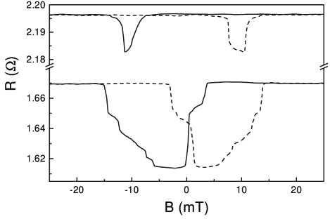
For the narrowest strip with a width of nm (see fig. 2) we do not observe any magneto resistance signal in parallel field, which is an indication that this electrode behaves as a single domain or reverses its magnetization by means of a fast domain wall sweep.
C Magneto resistance behavior of the Py/Cu contacts
A possible formation of a domain structure in the Py electrodes is important for a spin valve measurement, since the spin flip length of Py is very short ( nm, see VII) as compared to the domain size. In case of domain formation the magnetization direction of the injecting and detecting electrodes would be determined by the local domain(s) present at the Py/Cu contact area which could a have different magnetic switching behavior as the entire Py electrode.
Therefore we have locally measured the magneto resistance at the Py/Cu contact area, which we will call the ”contact” magneto resistance. For example the ”contact” magneto resistance of the Py electrode can be measured by sending current (see fig. 2) from contact to and measuring the voltage with contacts and . Note that in this geometry one is not sensitive for a spin valve signal, as only one Py electrode is used in the measurement.
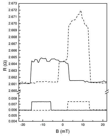
Figure 4 shows the ”contact” magneto resistance behavior at of three rectangular Py electrodes with dimensions: , and .
The ”contact” magneto resistance of the and nm wide electrodes show a similar magneto resistance behavior as the magneto resistance plots of the entire strips shown in fig. 3, except that there seems to be more asymmetry. For the nm wide electrode a ’positive’ peak is shown in the positive sweep direction and a ’negative’ peak in the negative sweep direction. This indicates that the magnetization reversal process is different for a positive and negative magnetic field sweep, resulting in different domain structures at the Py/Cu contact. However, it is important to note that amplitude of the ’contact’ magneto resistance can be as high as for the nm wide Py electrode. This magnitude is large as compared to the amplitude of the spin valve effect, as we will show in the next section.
For the nm wide Py electrode( bottom curve) a ”contact” magneto resistance behavior is observed, which appearance resembles much of a Hall signal, showing a difference in resistance at large negative and positive magnetic fields. A Hall voltage perpendicular to the substrate surface (z-direction) can be expected, as Py electrode is etched prior to the Cu deposition, causing the Cu wire to be a little bit ’sunk’ into the Py electrode. Changing one voltage probe from contact to contact (at the other side of the Py/Cu contact area, see fig. 2) produces the same signal. Also the signal amplitude of lies in the range of a Hall signal, which would have a maximum of , using a Cu Hall resistance of for a nm thick film and a maximal obtainable magnetic field change upon magnetization reversal of about T. When we take the position of the Hall step as the switching field at mT, we find a good agreement with the curling switching field mT for a width nm.
VI The Spin valve Effect
Two different measurement geometries are used to measure the spin valve effect in our device structure, the so called ’conventional’ geometry and ’non-local geometry. In the conventional measurement geometry the current is sent from contact to and the signal is measured between contacts and , see fig. 2. In the non-local measurement geometry the current is sent from contact to and the signal is measured between contacts and , see also fig. 1a. This technique is similar to the ”potentiometric” method of Johnson used in ref. VII. The difference between the two measurement geometries is that the conventional geometry suffers from a relatively large background resistance as compared to the spin valve resistance. The bad news is that this background resistance includes also small parts of the Py electrodes underneath the vertical Cu wires of the cross and the Py/Cu interface itself, which give rise to the ”contact” magneto resistance as was described in the previous section. Experimental measurements show that the spin valve signal can be completely dominated by the ”contact” magneto resistance of the Py eletrodes.
A Spin valve measurents
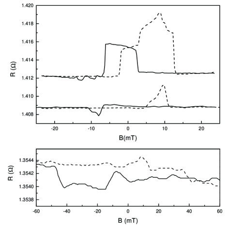
The measurements were performed by standard ac-lock-in-techniques, using current magnitudes of . The spin valve signals of two different samples (of the same batch) with a separation distance of nm are shown in fig. 5 and 6. The first sample, see fig. 5 had a current injector Py electrode of size , whereas the detector electrode had a size of . The second sample, see fig. 6 had narrower Py electrodes of and . This difference in width of the Py electrodes can be observed in the increased switching fields of the second sample.
From fig. 5 (top curves) we can see that the total magneto resistance signal in in the conventional geometry is about . The amplitude of the spin valve signal, measured in the non local geometry, is shown in the botton curve of fig. 5. Sweeping the magnetic field from negative to positive field, an increase in the resistance is observed, when the magnetization of Py1 flips at mT, resulting in an anti-parallel magnetization configuration. When the magnetization of Py2 flips at mT, the magnetizations are parallel again, but now point in the opposite direction. The magnitude of the spin valve signal measured in the non local geometry is (at K), much lower that the magneto resistance signal of measured in the conventional geometry. We therefore conclude that the ’contact’ magneto resistance of the and nm wide Py electrodes are completely dominating the magneto resistance signal in a conventional measurement geometry, making it impossible to detect a spin valve signal.
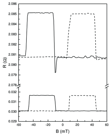
For the sample with Py electrodes of sizes and a spin valve signal can be observed in the conventional geometry. This is shown in the top curve of fig. 6. A small magneto resistance dip around mT can be observed in this sample upon switching from parallel to the anti-parallel magnetization configuration. The position of this peak in the magnetic field sweep and the amplitude of correspond to the ’contact’ magneto resistance behavior of the Py electrode, see fig. 4. However, after the magnetization of this Py electrode has switched, we do observe a resistance ’plateau’ up to a magnetic field of mT, where the second nm wide Py electrode switches. The magnitude of the spin valve effect measured in the conventional geometry is about . This is more than times bigger than the magnitude of the spin signal of (at K), measured in a ’non-local geometry, as shown in the bottom curve of fig. 6 (see also ref. VII). Calculations show (see VII, eq. 3) that the magnitude of the spin valve signal measured in a conventional geometry should be twice the magnitude of the spin valve signal measured in the non local geometry. At this moment we do not clearly understand why the measured ratio of the two spin signals is slightly larger than (factor of ).
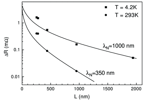
B Dependence on Py electrode spacing
A reduction of the magnitude of spin signal is observed with increased electrode spacing , as shown in fig. 7. By fitting the data to eq. 10 we have obtained in the Cu wire. From the best fits we find a value of at K, and nm at RT. These values are compatible with those reported in literature, where nm is obtained for Cu in GMR measurements at K[31]. However one should be careful to make a straightforward comparison between the GMR results and ours. In the thin films we use, the elastic mean free path of the electrons is limited by surface scattering, causing the conductivity of the Cu to be smaller than in GMR layers.
We can calculate the spin flip time in the Cu wire, using a Fermi velocity m/s [32]. At K we find ps, while at RT ps. Comparing the spin flip time to the elastic scattering time s at K, we find that on average the spin is flipped after about elastic scattering events in the Cu wire.
In principle the fits of fig. 7 also yield the spin polarization and the spin flip length of the Py electrodes. However, the values of and cannot be determined separately, as in the relevant limit () which applies to our experiment (), the spin signal is proportional to the product . From the fits we find that nm at 4.2 K and nm at RT. Taking, from literature [10], a spin flip length in the Py electrode of nm (at 4.2 K), a bulk current polarization of in the Py electrodes at K is obtained: . These values are in the same range as the results obtained from the analysis of the GMR effect.[2, 3, 10, 31]. However, the current polarization P at the interface of the current injecting Py electrode is much lower. Using eq.12, a polarization P for the samples with the smallest Py electrode spacing of nm at K is found to be only : . The reason for this reduction is caused by the unfavorable ratio of the ’small’ spin dependent resistance () and the ’large’ spin independent resistance (), which applies even in the absence of spin flip scattering events in the normal (Cu) metal.
VII conclusions
We have demonstrated spin injection and accumulation in a mesoscopic spin valve. We have shown that in conventional measurement geometry the magneto resistance effects of the injecting and detecting contacts can be much larger than the spin valve effect. These contact effects can be used to monitor the magnetization reversal process of the spin injecting and detecting contacts. In a non-local measurement geometry we can completely isolate the spin valve effect, as was reported earlier in ref. VII. Using this geometry we find a spin flip length in Cu of around at K and nm at RT. For the smallest Py electrode spacing, the magnitude of the spin signal and the current polarization P in the Cu wire are limited by the unfavorable ratio of the spin independent resistance of the Cu strips () and the spin dependent resistance of the Py ferromagnet ().
The authors wish to thank H. Boeve, J. Das and J. de Boeck at IMEC (Belgium) for support in sample fabrication and the Stichting Fundamenteel Onderzoek der Materie for financial support.
REFERENCES
- [1] R. Meservey and P. M. Tedrow, Physics Reports 238, 173 (1994).
- [2] M.A.M. Gijs and G.E.W. Bauer, Advances in Physics 46, 285 (1997)
- [3] J-Ph. Ansermet, J. Phys.:Condens. Matter 10, 6027 (1998)
- [4] F.J.Jedema, A.T. Filip, B.J. van Wees, Nature 410, 345 (2001).
- [5] A. Fert, and I.A. Campbell, J. de Physique, Colloques 32, C1-46 (1971)
- [6] P.C. van Son, H. van Kempen, and P. Wyder, Phys. Rev. Lett. 58, 2271 (1987)
- [7] T. Valet and A. Fert, Phys. Rev. B 48, 7099 (1993)
- [8] M. Johnson, and R.H. Silsbee, Phys. Rev. Lett. 55, 1790 (1985); M. Johnson and R.H. Silsbee, Phys. Rev. B 37, 5312 (1988)
- [9] M. Johnson, Phys. Rev. Lett. 70, 2142 (1993)
- [10] S. Dubois et al. Phys. Rev. B 60, 477 (1999); S.D. Steenwijk et al., J. Mag. Magn. Mater. 170 L1 (1997)
- [11] We expect the largest part of the magneto resistance signal to originate from the AMR effect. However we cannot exclude other (smaller) contributions, such as a possible domain wall resistance.
- [12] Th. G.S.M. Rijks, R. Coehoorn, M.J.M. de Jong and W.J.M. de Jonge, Phys.Rev.Lett. 51, 283 (1995)
- [13] K. Hong, N. Giordano, Phys. Rev. B, 51, 9855 (1995)
- [14] For a review see: M.E. Schabes, J. Magn. Magn. Mater. 95, 249 (1991)
- [15] E.C. Stoner, E.P. Wohlfarth, Philos. Trans. London Ser., A 240, 599 (1948), reprint: IEEE Trans. Magn. 27, 3475 (1991)
- [16] W. Wernsdorfer et al, Phys.Rev.Let. 77, 1873 (1996)
- [17] S.Pignard et al., J. Appl. Phys. 87, 824 (2000)
- [18] J-E Wegrowe et al., Phys. Rev. Lett. 82, 3681 (1999)
- [19] A.O. Adeyeye et al, J. Appl. Phys. 79, 6120 (1996), A.O. Adeyeye et al, Appl. Phys. Lett. 70, 1046 (1997)
- [20] Y. Q. Jia, S. Chou, J-G. Zhu, J. Appl. Phys, 81, 5461, 1997
- [21] F.G. Monzon, M.L. Roukes, J. Magn. Magn. Mater. 198, 632 (1999).
- [22] W.F. Brown Jr.,Phys. Rev. 105, 1479, (1957)
- [23] A. Aharoni, Phys. Stat. Sol. 16, 3, 9 (1966)
- [24] A. Aharoni, Appl. Phys. Lett. 82, 1281 (1997)
- [25] N. Smith, J. Appl. Phys. 63, 2932 (1988)
- [26] W. Wernsdorfer et al, Phys.Rev.B 53, 3341 (1996)
- [27] Y. Otani, K. Fuchamichi, O. Kitakami, Y. Shimada, B. Pannetier, J.P. Nozieres, T. Matsuda and A. Tonomura, Proc. MRS Spring Meeting, Symp. M (San Francisco) 1997
- [28] J. Yu, U. Rüdiger, A. D. Kent, L. Thomas and S. S. P. Parkin. Phys. Rev. B 60, pp. 7352-7358 (1999)
- [29] J. Nitta et al, J, Journ. Appl. Phys. xxxx, to be published
- [30] A. Filip et al, Phys. Rev. B 62, 9996 (2000)
- [31] Yang, Q. et al., Phys. Rev. Lett. 72, 3274-3277 (1994)
- [32] Ahscroft, N.W., Mermin, N.D. in Solid State Physics, W.B. Saunders Company, Orlando(1976).