Spin relaxation of conduction electrons in bulk III-V semiconductors
Abstract
Spin relaxation time of conduction electrons through the Elliot-Yafet, D’yakonov-Perel and Bir-Aronov-Pikus mechanisms is calculated theoretically for bulk GaAs, GaSb, InAs and InSb of both - and -type. Relative importance of each spin relaxation mechanism is compared and the diagrams showing the dominant mechanism are constructed as a function of temperature and impurity concentrations. Our approach is based upon theoretical calculation of the momentum relaxation rate and allows understanding of the interplay between various factors affecting the spin relaxation over a broad range of temperature and impurity concentration.
pacs:
PACS numbers: 72.25.Rb, 76.20.+q, 76.60.EsI Introduction
Recently, intensive experimental and theoretical efforts have been concentrated on the physics of electron spin due to the enormous potential of spin based devices. In these so called ”spintronic” devices,[1, 2, 3] information is encoded in the spin state of individual electrons, transferred with the electrons, and finally put under measurement. Electron spin states relax, i.e., depolarize, by scattering with imperfections or elementary excitations such as other carriers and phonons. Therefore, to realize any useful spintronic devices, it is essential to understand and have control over spin relaxation such that the information is not lost before a required operation is completed.
The investigation of spin relaxation has a long history dating back to the fifties and most studies have concentrated on III-V semiconductors since direct measurement of spin relaxation time is possible through optical orientation in these materials. Three main spin relaxation mechanisms, the Elliot-Yafet[4, 5] (EY), D’yakonov-Perel[6] (DP) and Bir-Aronov-Pikus[7] (BAP) mechanism have been suggested and confirmed experimentally. Earlier works for spin relaxation are mainly on bulk systems such as -GaAs,[8, 9, 10, 11] -GaSb,[12] GaAlAs[13] and -InSb.[14] More recently, spin relaxation has also been investigated in quantum well structures (GaAs,[15] GaAsSb,[16] InGaAs/InGaAsP[17] and GaAs/AlGaAs[18]) as well as in bulk systems (-GaAs[19, 20] and InAs[21]). On the theoretical side, there are recent approaches which refine or extend the original calculations of Refs. 3 and 4 to explain newly obtained experimental results. Flatté and coworkers[21, 22] employed a nonperturbative 14-band calculation for the DP mechanism both for bulk and quantum well structures and achieved a better agreement with the experimental results. The BAP process was reconsidered through a direct Monte Carlo simulation and extended to quantum wells by Maialle and coworkers.[23]
In the most studies, the strategy has been to find the relevant spin relaxation mechanism by comparing experimental results for spin relaxation time, , with theoretically predicted dependence on temperature or doping concentrations. Based upon these results, a “phase diagram”-like picture showing the dominant spin relaxation mechanism can be constructed to provide a comprehensive global understanding for competition of spin relaxation mechanisms. However, since available experimental results for are usually limited to a narrow range of external physical parameters except some intensively investigated materials, such pictures are currently available only for -GaAs and -GaSb.[12]
In this paper, we calculate the electron spin relaxation time for the EY (), the DP () and the BAP () processes for several bulk III-V semiconductors: GaAs, GaSb, InAs and InSb of both - and -type. Our result for is based upon theoretical calculation of the momentum relaxation time, . A diagram is constructed illustrating the dominant spin relaxation processes as a function of temperature and impurity concentration for each material. The resulting “phase diagrams” for -GaAs and -GaSb are in qualitative agreement with that of an earlier study.[12] The diagrams for the other materials considered in this work were not available in the literature and represent an attempt to provide a better understanding of interplay between various factors for . We also discuss some incomplete aspects of the current theories for spin relaxation.
The rest of this paper is organized as follows. In Sec. II the basic formulation of the three spin relaxation mechanisms is briefly described. The details of our calculation for the momentum relaxation time () and are presented in Sec. III. In Sec. IV the results for are compared with available experimental results and the “phase diagrams” for dominant spin relaxation is constructed. The conclusion follows in Sec. IV.
II Relevant Spin Relaxation Mechanisms
A Elliot-Yafet Mechanism
The EY mechanism originates from the fact that in the presence of spin-orbit coupling, the exact Bloch state is not a spin eigenstate but a superposition of them. This induces a finite probability for spin flip when the spatial part of electron wavefunction experiences a transition through scattering even if the involved interaction is spin independent.[4, 5] The spin relaxation time is given by[24]
| (1) |
where is the band gap and with the spin-orbit splitting of the valence band . is a dimensionless constant and varies from 2 to 6 depending on dominant scattering mechanism for momentum relaxation.
B D’yakonov-Perel Mechanism
In III-V semiconductors, the degeneracy in the conduction band is lifted for due to the absence of inversion symmetry. The resulting energy difference for electrons with the same but different spin states plays the role of an effective magnetic field and results in spin precession with angular velocity during the time between collisions. Since the magnitude and the direction of changes in an uncontrolled way due to electron scattering with impurities and excitations, this process contributes to spin relaxation. This is called the DP mechanism[6] and is given by[6, 24]
| (2) |
where is a dimensionless factor and ranges depending on the dominant momentum relaxation process. is the parameter characterizing the -term for conduction band electrons and is approximately given by
| (3) |
Here and are the effective mass of the conduction electron and the electron rest mass, respectively.
C Bir-Aronov-Pikus Mechanism
Electron spin flip transition is also possible by electron-hole scattering via exchange and annihilation interactions. This is called the BAP mechanism and is especially strong in -type semiconductors due to high hole concentrations. is given by several different expressions depending on the given external parameters. In the case of a nondegenerate semiconductor[7, 24] (),
| (4) |
where () is the concentration of free (bound) holes and is the critical hole concentration between degeneracy and nondegeneracy. is the conduction electron energy and is given by the relation
with the exchange splitting of the exciton ground state. and are defined as
where is the reduced mass of electron and hole, the Bohr radius ( 0.53 Å) and the Rydberg constant ( 13.6 eV). represents wavefunction describing the relative motion of electron with respect to hole and is the Sommerfeld factor given by
For degenerate case (), the result is[7, 24]
| (5) |
where is the hole effective mass and the hole Fermi energy, .
III Calculation
We first calculate the momentum relaxation time . We include
contributions from the polar optical phonon scattering (),
ionized impurity scattering (), piezoelectric scattering
(), and acoustic phonon deformation potential scattering
(). Our calculation of is performed with three
simplifying assumptions:
(a) the classical Boltzmann statistics is assumed for conduction electrons,
(b) the electrons are scattered in a parabolic band,
(c) the Mathiessen’s rule is applied so that .
Under these assumptions, can be obtained in a straightforward
way for the given material parameters of a III-V semiconductor.
According to the Ehrenreich’s variational calculation,[25] is obtained as
| (6) |
where and are the low- and high-frequency dielectric constants. is the longitudinal optical phonon frequency converted in the unit of temperature and is calculated as in Ref. 26 as a function of temperature and the free carrier density .
is described by the Brooks-Herring equation[27]
| (7) |
where is the concentration of minority impurities, i.e., acceptors for -type and donors for -type, and is a dimensionless quantity representing . is given by
with
is given by[28]
| (8) |
after spherical average of the piezoelectric and elastic constants over the zinc-blende structure is performed.[29] Here is the one independent piezoelectric constant and and are the average longitudinal and transverse elastic constants given by
The free carrier concentration (i.e., electrons for -type and holes for -type) is calculated from the equation
| (10) |
Here, is the majority impurity concentration. is given by , where represents for -type and for -type, respectively. is the ionization energy for majority impurity and is given by .
Table I shows the values of material parameters used in the calculation of and . is obtained by linearly interpolating or extrapolating and and is fixed to cm-3 in most cases. Figure 1 plots the results of mobility calculation, , for -GaAs and -InAs. Good agreement is obtained with the published result of Rode and Knight[32] for -GaAs while our result for -InAs shows a larger discrepancy up to 50% with those of Rode[33]. This seems to result from the fact that the nonparabolicity of conduction band, which we neglected, is stronger in InAs.
Figure 2 illustrates the dominant momentum relaxation mechanism for -GaAs as a function of temperature and impurity concentration. It is found that the contribution from the polar optical phonon scattering is dominant for the high-T and lightly-doped regime, while the ionized impurity scattering dominates otherwise. The same qualitative features are found for all other materials investigated, both for - and -type.
As was noted previously, both and include dimensionless factors, i.e., in Eq. (1) and in Eq. (2), which vary depending on the dominant momentum relaxation process. At the current stage, it is not clear how the crossover behavior is given quantitatively when there is a switch between two momentum relaxation processes. Therefore, we fix the dimensionless constants to their median values, i.e., and . This introduces 50 % uncertainty in our result for and . One might correct this error by directly looking into the dominant momentum relaxation process.
To calculate , we first need to identify the adequate regime for a given parameter set. is determined by the Mott criterion[31] where . The thermal averaged value of is obtained as
assuming a classical Boltzmann distribution for conduction electrons. On the other hand, the expressions for and in Eqs. (1) and (2) are after thermal averaging with respect to . A difficulty with the calculation of lies in the fact that there is no reliable data for , on which has the dependence of , for -InAs and -InSb. Therefore, we examine the tendency of as a function of as well.
IV Results and Discussion
We first compare the relative importance of each spin relaxation mechanism. Figure 3 shows the dominant spin relaxation processes for -type GaAs, GaSb, InAs and InSb. For -type semiconductors, the contribution of the BAP mechanism is negligible since the equilibrium hole concentration is extremely small. Therefore, we watch the competition between the EY and the DP processes. As shown in Fig. 3, it turns out that for all materials investigated there exists a transition from the DP-dominant regime to the EY-dominant regime at 5 K as the temperature is lowered. These results are consistent with the previously published results that the DP process is the relevant spin relaxation mechanism for -GaAs[19, 22] and -InAs[21] at high temperature of 300 K and that the EY process is relevant for -InSb at low temperature of T = 1.3 K.[14] When the acceptor, i.e., the minority impurity, concentration decreases, we find that the DP-dominant regime enlarges. This can be understood from following consideration. The acceptors in -type materials are always ionized and the decrease in the acceptor concentration corresponds to the decrease in the number of scattering centers for ionized impurity scattering procedure, which is the main momentum relaxation mechanism at low temperature. Therefore, a larger results as the acceptor concentration decreases and this induces a larger and a smaller since and .
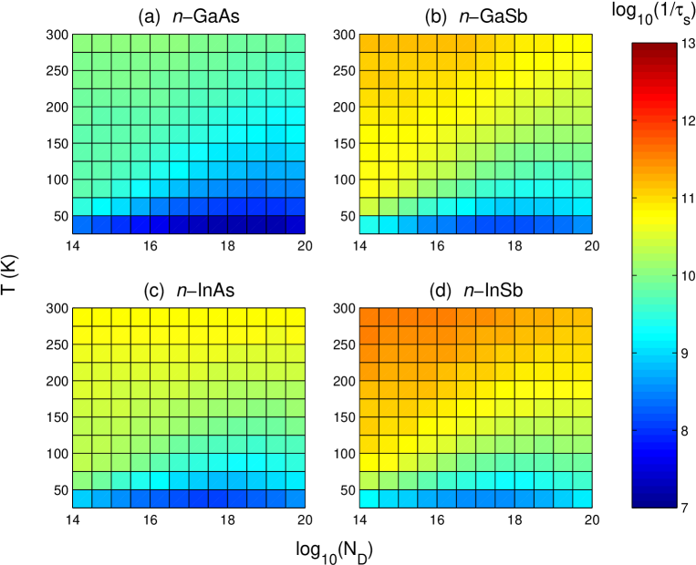
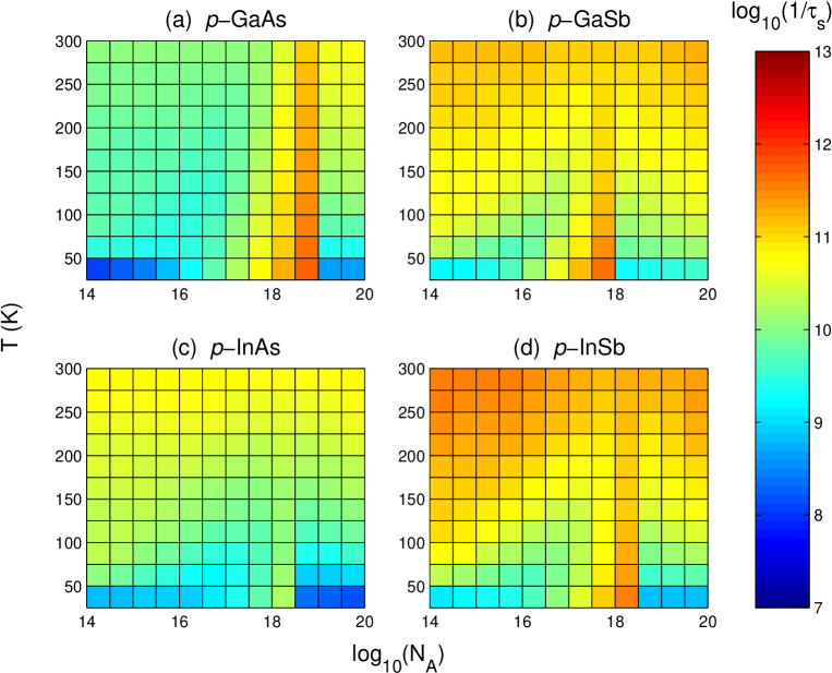
The diagrams for -type materials are illustrated in Fig. 4 with cm-3 cm-3 and cm-3. For -type materials, no systematic changes are found when the minority carrier concentration is varied. For -GaAs and -GaSb, we find that the BAP (DP) is dominant in the low-T (high-T) and high (low) doping regime. This is in qualitative agreement with the results of Aronov et al.,[12] in which diagrams of the same idea were constructed based on experimental results. For -InAs, a similar feature to those of -GaAs and -GaSb is found for = 10 eV, and as decreases, the BAP dominant regime becomes smaller. For -InSb, we obtain similar results to those for -InAs as a function of . Figure 4(d) shows the case of 0.2 eV where a BAP-dominant regime exits at 100 K and intermediate doping concentrations. We find abrupt discontinuities in at , which results in unphysical sharp cusps at cm-3 in Fig. 4. This is an artifact resulting from the fact that no quantitative expression for is available for the crossover between nondegenerate [Eq. (4)] and degenerate [Eq. (5)] hole regimes. Experimentally, it was found that there exists an intermediate regime at where remains nearly flat with respect to the change in and that the range of such intermediate regime varies depending on the material.[12]
Figures 5 and 6 provide the total spin relaxation time, i.e., for -type and for -type, respectively. ranges from 1 ps to 100 ns for -type materials and from 0.1 ps to 10 ns for -type materials, respectively, over the parameter space shown in Figs. 5 and 6. For -type materials, increases as decreases with the longest found at cm-3 instead of in purer materials. This is because the regime shown in Fig. 5 is dominated solely by the DP-process and , which is proportional to , increases as the impurity concentration decreases. The same qualitative feature has also been found in a recent experiment.[19] In our result for -GaAs, ranges from 5 ns to 60 ns for = 25 K, which gives a reasonable agreement with the experimental result of Ref. 19 ( 70 ns at = 20 K). As for -InAs with cm-3 and = 300 K, our result gives = 12 ps which compares very well with a recent experimental result of ps.[21]
At lower temperature, we find a discrepancy with recent experimental result for -GaAs. In experiment[19] 100 ns at 5 K for cm-3 was reported, while our result predicts a larger value of ns. Reference. 19 suggested that the main spin relaxation at this low temperature regime is due to the EY mechanism. According to our result, however, since 1 ps and and are given by ns and ns, respectively, neither the EY nor the DP mechanism provides a satisfactory explanation for the experimental result. Very recently, in ref. 20, spin relaxation time of 290 30 ns at 4.2 K was reported for bound electrons to donors in -GaAs and the relevant spin relaxation mechanism was proposed to be the hyperfine interaction with nuclei,[37] which was not taken into account in our current work. A further research incorporating this effect is needed to resolve the discrepancy between our result and the experimental result of Ref. 19.
In -type materials, smaller , i.e., stronger spin relaxation rate, than that in -type materials is found due to the effect of the BAP process. The strong discontinuities at are also noticeable in Fig. 6 due to the incompleteness of the BAP expressions given by Eqs. (4) and (5), as mentioned earlier.
V Conclusion
In this paper, we calculated theoretically for several bulk
III-V semiconductors and compared the contributions from the
three main spin relaxation mechanisms as a function of temperature
and donor/acceptor concentrations. In -type materials, the
DP mechanism is found to be dominant down to very low temperature,
below which the EY mechanism dominates. While our calculated
spin relaxation times are in reasonable agreement with the
experimental results for high temperature regime of 20 K, there exists a discrepancy at 5 K for
-GaAs. Further theoretical efforts incorporating other spin
relaxation mechanisms neglected in this paper are needed for
its resolution. As for -type materials, the BAP (DP) mechanism
is dominant at low (high) temperature and high (low) acceptor
concentrations. We find that the
crossover between various regimes for spin relaxation requires a
further
theoretical investigation for a more thorough understanding and
realistic comparison with experimental data. This is especially the
case for the crossover between nondegenerate and degenerate hole
regimes for the BAP process.
Acknowledgment
We are thankful to M. I. D’yakonov for critical comment and to J. M. Kikkawa for useful discussion. This work is supported by the Office of Naval Research and the Defense Advanced Research Projects Agency.
REFERENCES
- [1] D. DiVincenzo, Science 270, 255 (1995).
- [2] G. Prinz, Phys. Today 48, 58 (1995).
- [3] L. Sham, Science 277, 1258 (1997).
- [4] R. J. Elliot, Phys. Rev. 96, 266 (1954).
- [5] Y. Yafet, in Solid State Physics, edited by F. Seitz and D. Turnbull (Academic, New York, 1963), Vol. 14.
- [6] M. I. D’yakonov and V. I. Perel, Sov. Phys. JETP 33, 1053 (1971); Sov. Phys. Solid State 13, 3023 (1972).
- [7] G. L. Bir, A. G. Aronov, and G. E. Pikus, Sov. Phys. JETP 42, 705 (1976).
- [8] A. H. Clark, R. D. Burnham, D. J. Chadi, and R. M. White, Solid State Commun. 20, 385 (1976).
- [9] G. Fishman and G. Lampel, Phys. Rev. B 16, 820 (1977).
- [10] V. I. Maruschak, M. N. Stepanova, and A. N. Titkov, Sov. Phys. Solid State 25, 2035 (1983).
- [11] K. Zerrouati, F. Fabre, G. Bacquet, J. Bandet, J. Frandon, G. Lampel, and D. Paget, Phys. Rev. B 37, 1334 (1988).
- [12] A. G. Aronov, G. E. Pikus, and A. N. Titkov, Sov. Phys. JETP 57, 680 (1983).
- [13] A. H. Clark, R. D. Burnham, D. J. Chadi, and R. M. White, Phys. Rev. B 12, 5758 (1975).
- [14] J. N. Chazalviel, Phys. Rev. B 11, 1555 (1975).
- [15] Y. Ohno, R. Terauchi, T. Adachi, F. Matsukura, and H. Ohno, Phys. Rev. Lett. 83, 4196 (1999).
- [16] K. C. Hall, S. W. Leonard, H. M. van Driel, A. R. Kost, E. Selvig, and D. H. Chow, Appl. Phys. Lett. 75, 4156 (1999).
- [17] J. T. Hyland, G. T. Kennedy, A. Miller, and C. C. Button, Semicond. Sci. Technol. 14, 215 (1999).
- [18] A. Malinowski, R. S. Britton, T. Grevatt, R. T. Harley, D. A. Ritchie, and M. Y. Simmons, Phys. Rev. B 62, 13034 (2000).
- [19] J. M. Kikkawa and D. D. Awschalom, Phys. Rev. Lett. 80, 4313 (1998).
- [20] R. I. Dzhioev, B. P. Zakharchenya, V. L. Korenev, D. Gammon, and D. S. Katzer, JETP Lett. 74, 182 (2001).
- [21] T. F. Boggess, J. T. Olesberg, C. Yu, M. E. Flatté, and W. H. Lau, Appl. Phys. Lett. 77, 1333 (2000).
- [22] W. H. Lau, J. T. Olesberg, and M. E. Flatté, Phys. Rev. B 64, 161301 (2001).
- [23] M. Z. Maialle, Phys. Rev. B 54, 1967 (1996); M. Z. Maialle and M. H. Degani, Appl. Phys. Lett. 70, 1864 (1997); M. Z. Maialle and M. H. Degani, Phys. Rev. B 55, 13771 (1997).
- [24] G. E. Pikus and A. N. Titkov, in Optical Orientation, edited by F. Meier and B. P. Zakharchenya (North-Holland, Amsterdam, 1984).
- [25] H. Ehrenreich, Phys. Rev. B 120, 1951 (1960).
- [26] H. Ehrenreich, J. Phys. Chem. Solids 8, 130 (1959).
- [27] H. Brooks, Adv. Electron. Electron Phys. 7, 158 (1955).
- [28] H. J. G. Meijer and D. Polder, Physica 19, 255 (1953).
- [29] J. D. Zook, Phys. Rev. 136, A869 (1964).
- [30] J. Bardeen and W. Shockley, Phys. Rev. 80, 72 (1950).
- [31] P. P. Edwards and M. J. Sienko, Phys. Rev. B 17, 2575 (1978).
- [32] D. L. Rode and S. Knight, Phys. Rev. B 3, 2534 (1971).
- [33] D. L. Rode, Phys. Rev. B 3, 3287 (1971).
- [34] Landolt-Börnstein Numerical Data and Functional Relationships in Science and Technology, edited by O. Madelung, M. Schultz, and H. Weiss, New series, Vol. 17 (1982); reprinted in O. Madelung, editor, Semiconductors-Basic Data, 2nd. ed. (Springer, New York, 1996).
- [35] E. Haga and H. Kimura, J. Phys. Soc. Japan 19, 658 (1964).
- [36] D. D. Sell, Surf. Sci. 35, 863 (1973).
- [37] A. Abragam, The Pricnciples of Nuclear Magnetism (Clarendon, Oxford, 1961).
| GaAs | GaSb | InAs | InSb | |
| 0.065 | 0.0412 | 0.023 | 0.0136 | |
| 0.5 | 0.28 | 0.43 | 0.45 | |
| (eV) | 0.341 | 0.75 | 0.38 | 0.85 |
| (eV) | 1.52 (0 ) | 0.822 (0 ) | 0.418 (4.2 ) | 0.235 (1.8 ) |
| (eV) | 1.42 (300 ) | 0.75 (300 ) | 0.354 (295 ) | 0.23 (77 ) |
| 12.515 | 15.69 | 15.15 | 16.8 | |
| 10.673 | 14.44 | 12.25 | 15.68 | |
| 410 | 335 | 343 | 280 | |
| (dyn/cm | 1.221 | 8.834 | 8.329 | 6.669 |
| (dyn/cm | 5.66 | 4.023 | 4.526 | 3.645 |
| (dyn/cm | 5.99 | 4.322 | 3.959 | 3.02 |
| (V/cm) | 1.45 | 9.5 | 3.5 | 4.7 |
| (eV) | ||||
| (eV) | unknown | unknown | ||
| (cm | 7.53 | 6.71 | 2.7 | 2.27 |
aRef. 35. bRef. 33. cRef. 36. dRef. 12.