Large magnetoresistance effect due to spin-injection into a non-magnetic semiconductor
Abstract
A novel magnetoresistance effect, due to the injection of a spin-polarized electron current from a dilute magnetic into a non-magnetic semiconductor, is presented. The effect results from the suppression of a spin channel in the non-magnetic semiconductor and can theoretically yield a positive magnetoresistance of 100%, when the spin flip length in the non-magnetic semiconductor is sufficiently large. Experimentally, our devices exhibit up to 25% magnetoresistance.
Semiconductor spintronics has gained a strong boost from the recent experimental demonstration of electrical spin injection into a non-magnetic semiconductor (NMS), using Dilute Magnetic Semiconductors (DMS) as spin-injecting contacts[1, 2]. However, the practical implications of these achievements for utilizing spin injection in semiconductor circuits are still limited, since in both experiments the spin polarization of the current was detected via the circular polarization of the electroluminescence of a semiconductor light emitting diode, and no appreciable effect of the spin polarization on the resistance of the device could be observed. Evidently, such an effect would be extremely useful for the implementation of spin injection in semiconductor transport devices for memory and logic applications. An obvious candidate for implementing a spin-dependent resistance in a semiconductor device is based on utilizing the Giant Magneto Resistance (GMR) effect, which is well known from all-metal ferromagnetic/non- magnetic multilayer devices[3]. However, the practical realization of a semiconducting GMR device has proven to be difficult, mainly because the effect relies on utilizing ferromagnetic contacts. We now know[4] that spin-injection into semiconductors can only be achieved from a contact that has a similarly low conductance as the non-magnetic semiconductor, and a close to 100 % spin-polarization. This excludes using ferromagnetic metals like Fe, Co, or Ni as contact materials. As shown in [1], II-VI-DMSs do fulfill the 100% polarization requirement [4] and provide a solid means for generating a strongly spin-polarized current in a NMS.
We have now found that the tunable Zeeman-splitting in these paramagnetic DMSs allows for the realization of a novel magnetoresistance effect. The effect (a large positive magnetoresistance) is caused by the suppression of one spin channel in the NMS. In this paper we describe the observation of the novel effect.
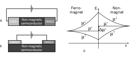
Consider a device where a NMS layer is fitted with two paramagnetic DMS-contacts which can be either non-magnetized or magnetized in parallel by a suitable external field (Fig. 1a). In such a device, the current will be either unpolarized (non-magnetized contacts) or spin-polarized (magnetized contacts). In an NMS, electrons with spin-up and spin-down each contribute one half of the conductivity of the non-magnetic semiconductor. Their transport can be regarded as occurring through separate ’spin channels’, as long as the device dimensions are shorter than the spin scattering length. When the current injected into the NMS becomes spin-polarized, e.g. by magnetizing the DMS contacts, this implies that both spin channels in the NMS carry a different amount of current. Because the conductivity of the spin channels is equal, injecting a spin-polarized current - or, in other words, not using the conductivity of one of the available spin channels - implies that the total device resistance increases. The effect can be as large as 100% for complete spin-polarization when only one of the two spin channels in the NMS is used. We have performed a more detailed modeling of the device resistance using the local approach described in Refs. [4, 5], and find that in a one dimensional device (Fig. 1a) the resistance change is given by
| (1) |
where are the spin flip length and the conductivity in the DMS and the NMS respectively, is the spacing between the contacts and is the degree of spin polarization in the bulk of the contacts. is given by .
Eq. (1) describes a magnetoresistance effect due to spin accumulation in a non-magnetic material, similar to the situation for GMR. However, the effect is distinct from GMR in several aspects.
The GMR effect only occurs in the limit , and corresponds to the difference in resistance between the blocking of one spin channel at the detector (for parallel magentization of injector and detector), and two blocked spin channels (for antiparallel magnetization). The paramagnetic effect in this limit results from the difference in device resistance between zero blocked channels (for unmagnetized DMS) and one blocked channel. In the limit of the maximum increase in resistance for is indeed which is equivalent to a doubling of the resistance of the NMS.
Much more striking perhaps is that from Eq. (1) one readily finds that a magnetoresistance effect still exists when . In principle, also a device with only one magnetic contact will show the effect - in contrast with GMR. In this limit, the suppression of the spin channel occurs only over a distance of order of the spin flip length. The behaviour of the electrochemical potentials of the spin channels near the DMS/NMS contact in that case is sketched in fig. 1c, where the discontinuity in the average potential at the DMS/NMS interface is equivalent to the boundary resistance of a ferromagnet/nonferromagnet metal interface described by van Son et al.[5] and by Johnson and Silsbee[6]. Our DMS contacts allow for a continuous tuning of the boundary resistance, which obviously cannot be easily realized with ferromagnetic contacts and basically constitutes the magnetoresistance effect in this limit - the field-induced surplus resistance is directly related to an increase on boundary resistance. In the experiments described below, we only employ a geometry with two DMS contacts. This is solely because of technological reasons, but implies that for samples where , the data simply reflect the change in boundary resistance of two independent DMS/NMS contacts.
For an experimental demonstration of the novel magnetoresistance effect, we have used MBE-grown II-VI-semiconductor multilayer structures, consisting of a n-doped Zn0.97Be0.03Se layer (thickness 500 nm) as a NMS, contacted by the DMS Zn0.89Be0.05Mn0.06Se (thickness 100 nm or 200 nm) , grown on an insulating GaAs substrate. Devices were fabricated for a variety of doping levels above the metal-insulator transition (which is around cm-3 for these materials), i.e. aiming for nominal donor concentrations of 1, 3 and 9 cm for both NMS and DMS, in all possible combinations. The actual dopant concentrations were determined from Hall measurements on appropriate control samples. Contact pads (m) positioned at various spacings (m or more) were defined lithographically in a 100 nm Al layer, which was deposited on top of the semiconductor stack to provide an ohmic contact to the DMS. These pads were then used as an etch mask for wet chemical etching, removing the magnetic semiconductor and some 10 nm of the Zn0.97Be0.03Se in the unmasked area. In a second optical lithography step, a mesa area including two of the DMS contact pads was defined, and the surrounding Zn0.97Be0.03Se was removed by wet chemical etching. The resulting structure is drawn schematically in Fig. 1b. The magnetoresistance of a large number of devices was measured at several different temperatures and for fields between 0 and 7 T, using an AC voltage bias of 100 V (25 V for mK). Care was taken to ensure that the data were within the regime of linear response.
In the experiment, all Zn0.89Be0.05Mn0.06Se / Zn0.97Be0.03Se hybrid structures exhibited a strong positive magnetoresistance. Here, we will focus on two series of data that prove that the magnetoresistance behaviour is caused by the effect introduced above; the data are representative for all devices studied so far.
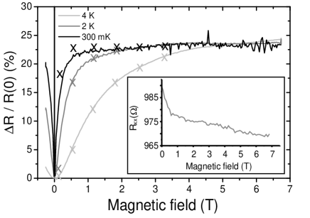
Typical traces of the effect and its temperature dependence are shown in Fig. 2 for a device with a contact spacing of 20m, a doping level of (DMS) and (NMS), and a DMS thickness of 100 nm. The maximum change in resistance is up to 91 , with a total device resistance of 376 . A lower limit for the relative change in resistance is 25%, which is a conservative estimate because we neglected the contributions of contact resistances between metal and DMS (Correcting for the contact resistance, which is known because the samples were actually fabricated in a transmission line configuration, would yield a change of more than 30%). We have verified that the effect does not depend on the orientation of the magnetic field. As is also evident from fig. 2, reducing the temperature does not affect the saturation value, however, the saturation field is strongly reduced - much stronger than one typically would expect from the temperature dependence of the Zeeman splitting in the DMS. This observation reflects the strongly non-linear dependence [4] of the spin injection efficiency on the spin-polarization in the DMS. An exact modeling of the temperature dependence is not straight-forward because of the unknown field- and temperature dependence of and . Moreover, since Eq. (1) was derived for the one-dimensional device of Fig. 1a and does not apply to the essentially two-dimensional devices studied experimentally (Fig. 1b), any fits of actual data to this expression have only a limited validity. Bearing all of this in mind, the crosses in Figure 2 indicate the behaviour predicted by Eq. (1), assuming and to be temperature independent, and fitted to the magnetoresistance behaviour at 4 K. The crosses for the other temperatures were obtained simply by assuming a Boltzmann distribution of the conduction electrons between the Zeeman levels, i.e., neglecting band-filling effects[9] while keeping the other parameters constant. Evidently, Eq. (1) gives a reasonable description of the actually observed device behaviour. However, we should note that below 0.3 T the fit to the experiment is less accurate.
Actual values for the free parameters in Eq.(1) can be obtained from the saturation magnetoresistance using cm-1 and cm, as obtained from control samples, yielding nm and m. The spin polarization in the DMS is deduced from the Zeeman splitting as obtained from optical experiments. The values for the spin scattering length obtained from this fit seem quite reasonable; is of a similar magnitude as the values usually encountered for ferromagnetic metals, and agrees well with optical data by Kikkawa et al.[10].
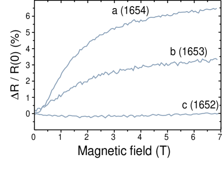
Fig. 3 displays experimental results obtained for a series of devices with doping levels , , leading to conductivities cm-1 and cm-1, a contact spacing of 10m, and a DMS thickness of 0, 100 and 200 nm. From these data, three major features are apparent. First, the maximum size of the relative magnetoresistance effect is reduced to about 6%. This can be explained by the increased spin scattering in the higher doped NMS.[10] Second, reducing the DMS thickness from 200 (fig. 3a) to 100 nm (fig. 3b) results in a reduction of the relative effect by a factor of 2. This observation can be understood by realizing that, due to the finite spin scattering length in the DMS, a thinner DMS layer results in a lower degree of spin polarization, again showing that the effect is quite sensitive to even a small number of electrons in the upper Zeeman level. Finally, curve (c) was measured for a reference device where the DMS layer was omitted. In this case, only a small () negative magnetoresistance is observed, possibly due to weak localization effects. This observation clearly evidences that spin injection via the DMS layer is an absolute necessity to observe the novel magnetoresistance effect. Using Eq. (1) and the conductivities quoted above, we can consistently reproduce the observed DMS thickness-dependence of the effect for nm and m, which again is in line with the observed[10] decrease of spin scattering length with increasing dopant concentration in highly doped samples.
The high dopant concentration in the DMS layers in the devices of Figs. 2 and 3 was chosen to guarantee that the intrinsic magnetoresistance of the DMS is negative. At lower n (but above the metal-insulator transition), DMSs show an additional positive magnetoresistance due to the e-e correction to the conductivity. This correction vanishes with increasing , according to [11], where is the wavevector at the Fermi energy and is the mean free path of the electron. That we are indeed in the limit where only the weak localization correction to the conductivity remains is evidenced by the small negative magnetoresistance (2%) of a sample consisting only of DMS (Fig. 2, insert).
In order to better understand the device behavior and the magnitude of the effect, we have performed two dimensional simulations of the current flow in the device based on the drift-diffusion equation and incorporating the model of reference[4]. The details of these calculations will be presented elsewhere, but here we will summarize the main findings relevant to the present paper.
(i) Because of the relatively low conductivity in the DMS layer, the current into the NMS layer is injected perpendicular to the DMS/NMS interface across the whole width (200) of the contact pad. As already indicated above, this raises questions on the validity of using Eq. (1) for extracting material parameters from the actual measurements.
(ii) Because of this current profile, the resistivity of the DMS layer contributes only on the order of 2% to the total device resistance. This implies that the intrinsic magnetoresistance of the DMS (Fig. 2-insert) can be neglected when describing the overall device magnetoresistance.
(iii) The total device resistance is mainly determined by the region under the contact which is close to the DMS/NMS interface.
(i) and (iii) together imply that one can have sizeable magnetoresistance effects, even when the spin-scattering length is in the sub-micron regime, but cannot expect to see a dependence of the effect on the spacing between the contacts. In order to observe the latter, one needs to fabricate sub-micron contacts on a micrometer sized mesa. However, such a technology does not yet exist.
Given the small and negative magnetoresistance measured for the reference layers (Fig. 2-insert, 3), we conclude that our experimental data on the multilayer samples directly evidence that we have succeeded in observing the novel, spin-injection-induced, magnetoresistance effect described above. Note that in contrast to Ref. [1] the data presented here were all taken in the regime of linear response. They represent a very strong evidence for the single-particle character of the electrical spin injection from a DMS and confirm the validity of Ref. [4, 5, 6] in describing the injection phenomena. The strong temperature dependence of the saturation behavior in a regime where the giant Zeeman splitting is almost temperature-independent is further evidence that the polarization in a diffusive spininjector has to be very close to unity in order to achieve efficient spin injection. At the same time, our data demonstrate a new magnetoresistance effect which can be regarded as the paramagnetic version of GMR. The results illustrate a viable route towards a straightforward determination of spin polarization in semiconductor devices. Using spin dependent resistance effects spin controlled programmable logic may become feasible; other applications could be found in read-in and read-out mechanisms for solid state quantum-computing with spins.
Acknowledgements.
We acknowledge the financial support of the Bundesministerium für Bildung und Forschung and the European Commission. We would also like to thank V. Hock, N. Schwarz, T. Dietl, and G. E. W. Bauer for help and discussions.REFERENCES
- [1] R. Fiederling et al., Nature (London) 402, 787 (1999);
- [2] Y. Ohno et al., Nature (London) 402, 790 (1999).
- [3] M. N. Baibich et al., Phys. Rev. Lett. 61, 2472 (1988); G. Binasch, P. Grünberg, F. Saurenbach, W. Zinn, Phys. Rev. B 39, 4828 (1989)
- [4] G. Schmidt, D. Ferrand, L. W. Molenkamp, A. T. Filip, B. J. van Wees, Phys. Rev. B 62, R4790 (2000).
- [5] P. C. van Son, H. van Kempen, P. Wyder, Phys. Rev. Lett. 58(21), 2271 (1987).
- [6] M. Johnson, and R.H. Silsbee, Phys. Rev. B 35, 4959 (1987); Phys. Rev. Lett. 60, 377 (1988).
- [7] J. K. Furdyna, J. Appl. Phys. 64, R29 (1988).
- [8] For technological reasons, an exact realization of the one-dimensional device in fig. 1a is not feasible; the main problem is the high contact resistance between Al and the II-VI compounds.
- [9] This approximation is not straightforward. When one assumes a parabolic conduction band in the DMS, the doping levels used here would imply a Fermi energy of order tens of meV, comparable to or larger than the Zeeman splitting of the conduction band, and leading to reduced spin polarization. This is in contradiction with our experimental results on the spin diode (Ref. 1). However, since the DMSs are doped much above the Mott criterium, the parabolic band model is not applicable. The metallic side of the Mott transition directly implies the existence of an impurity band, which has a much higher density of states than one would estimate from a parabolic band model. Temperature-dependent transport measurements by our group support the existence of an impurity band.
- [10] J.M. Kikkawa, I.P. Smorchkova, N. Samarth, and D.D. Awschalom, Science 277, 1284 (1997); J.M. Kikkawa, and D.D. Awschalom, Phys. Rev. Lett. 80, 4313 (1998).
- [11] M. Sawicki, T. Dietl, in: Proceedings of the 19 th International Conference on the Physics of Semiconductors, 1217 (Publisher: Institute of Physics, Polisch academy of sciences, Warsaw, Poland 1979).
- [12] J. A. Gaj, R. Planel, G. Fishman, Solid State Comm. 29, 435 (1979).