Image-potential band-gap narrowing at a metal/semiconductor interface
Abstract
GW approximation is used to systematically revisit the image-potential band-gap narrowing at metal/semiconductor interfaces proposed by Inkson in the 1970’s. Here we have questioned how the narrowing as calculated from quasi-particle energy spectra for the jellium/Si interface depends on of the jellium. The gap narrowing is found to only weakly depend on (i.e., narrowing eV even for a large . Hence we can turn to smaller polarizability in the semiconductor side as an important factor in looking for larger narrowing.
pacs:
PACS numbers: 73.30.+y, 73.40.SxI Introduction
Disrupted translational symmetry at surfaces and interfaces provides a potentially rich playing ground for many-body effects. A seminal proposal was in fact made by Inkson back in the 1970’s, who proposed that a metal-insulator transition can take place around the interface.[1, 2, 3, 4, 5] Classically, his argument is as follows. When a metal is placed on top of a semiconductor, an electron in the semiconductor feels an image potential which is the interaction between the particle and its image charge in the metal. This leads to a downward bending of the conduction band bottom toward the interface, ), where is the dielectric constant of the semiconductor and is the distance from the interface. Similarly, the valence band top is bent upward by the same amount.
Quantum mechanically, this becomes as follows[4]. The contribution of the correlation term to the self-energy of the electron in the semiconductor is similar () for the conduction and valence bands. On the other hand, while the screened exchange term almost vanishes for the conduction band, it amounts to () for the valence band. As a result, while the conduction band bends downward like ), the valence band bends upward like ). This kind of band bending can occur over short distances ( Å), while the usual Schottky barrier occurs over much larger distances ( Å).
After the proposal of Inkson was made, various studies for the band gap reduction or closure at metal/semiconductor(insulator) interfaces have been performed theoretically and experimently[6, 7, 8, 9]. Recently, Murata et al[6] have studied Ru(0001)/Al2O3 and have observed the band gap narrowing of Al2O3. Kiguchi et al[7] have studied LiCl films on Cu(001), and have found that 3p level of Cl shift up to the Fermi level as the number of LiCl layers decreases.
As for the first principles many body calculation, Charlesworth et al.[9] have calculated the quasiparticle electronic structure of Al/GaAs(110), and have shown the band gap narrowing for the first time. The amount of the band gap reduction turned out to be about 0.4 eV.
A big issue remains however: which combination of metal and semiconductor will favor the local metal-insulator transition? As a first step toward such studies, we should investigate how the band gap reduction depends on the density of electrons (as represented by ) in the metallic side, which governs the electron correlation in that side. The value of in metals in fact extends over a wide range, 1.8 5.6, and the image-potential effect in metals with greater is expected to be smaller than that for a smaller , a value corresponding to Al and assumed by Charlesworth[9]. If the band gap narrowing still occurs significantly for metals with larger , we can turn our attention to the semiconductor side in optimizing the local metal-insulator transition.
This is exactly the purpose of the present paper, i.e., to discuss the dependence of the band gap reduction quantitively. Since governs the dielectric response, the image-potential effect may well depend sensitively on , which is why we have to look into the dependence from first principles. For that purpose we have to go beyond the usual local density functional approximation (LDA), since we are talking about the effects of screening. So here we adopt what is called the GW approximation, which is roughly the RPA (random-phase approximation) + LDA.
II Model
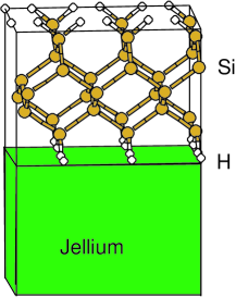
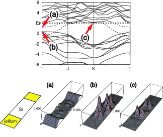
To focus on the problem described above, we can simplify the metallic side into the jellium model. On the other hand, we have to have an atomistic model for the semiconductor side, since we are questioning effects occurring on the length scale of few atomic spacings on this side. So the model is depicted in Fig.1. To facilitate the band calculation, we adopt a repeated-slab model (periodic boundary condition), in which the semiconductor slabs alternate with the jellium slabs. We calculate the band structure in the - space.
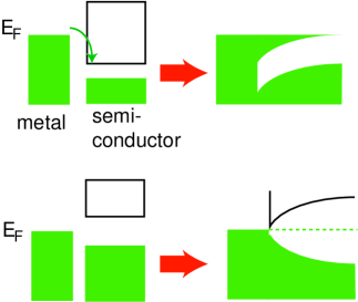
When a semiconductor and a metal are put together, the Fermi energies in the metal and semiconductor have to be aligned in thermal equilibrium, which implies that some charges should flow across the interface resulting in a charged region on the semiconductor side in general (in the absence of impurity levels in the semiconductor gap). This charge redistribution creates an electrostatic potential, and this bends the valence and conduction bands of the semiconductor, which becomes significant at distances Å. Since what we want to look at is the physics on the scale of Å, we can neglect this bending (unless the charge rearrangement is drastic). In fact, Charlesworth et al.[9] have estimated the effect of the charge redistribution for Al/GaAs(110), where electrons flow from Al with a higher Fermi energy to the lower conduction band bottom in GaAs, and found the effect to be negligible. However, when the charge rearrangement occurs drastically, this one-body effect can become serious. Thus, to focus on the image-potential effect we have to exclude the one-body potential effect carefully. For this purpose, we set the Fermi energy of the metal inside the energy gap of the semiconductor(Fig.2). As we shall show, such a situation is indeed realized if we take an appropriate value of for the jellium model.
As for the semiconductor side, we have employed a slab, which consists of five layers of Si atoms stacked in the [001] direction. To get rid of complications arising from dangling bonds, the edges are terminated by hydrogen atoms. For the structure of the hydrogen-terminated surface, we assume for simplicity a non-reconstructed one (). With this assumption we have optimized the structure imposing the mirror-plane symmetries (along [100] and [010]) and an inversion+mirror symmetry ([001]). The hydrogen atoms are allowed to relax in any directions. The size of a supercell is 7.182 30.48 a.u.3 along the , with the thickness of the jellium being 12.51 a.u.
The band gap narrowing or closure in the semiconductor is probed here by identifying the character of the wave functions for various bands for the repeated slab model: by concentrating on the bands whose wave functions have their amplitudes primarily on the semiconducting side we can define the gap of the semiconductor.
III Method
Band-structure calculations are usually performed within the framework of the LDA. In this formalism, many-body effects are represented by the so-called exchange-correlation potential, which is a functional of the electron density. In practice, this potential is approximated as a function of the local density, and we have the LDA.
While the density-functional formalism is shown to be rigorous for the ground state[10] and LDA gives reliable information about the ground state properties for various electron systems, it is well-known that these approaches are not useful for excited states. In fact, LDA usually underestimates the band gap of semiconductors and insulators. Moreover, LDA cannot be applied to the cases where the electron density varies in space.
Still, LDA wave functions are usually good approximation to quasi-particle wave functions[11]. Since excitations can be described by many-body perturbation theory, it should be quite a good starting point to adopt the LDA wave functions as the basis for the many-body perturbation theory in determining the self-energy and spectrum of the quasi-particles.
For the calculation of the self-energy, various approximations have been developed. Among them, Hedin’s GW approximation[12, 13] often gives excellent quasi-particle energies in bulk semiconductors with a comparatively simple formalism[11, 14]. The GW approximation essentially amounts to the RPA in the LDA formalism, so we have adopted this method to study the image-potential band-gap reduction.
A LDA
So the first task in the present study is to perform an LDA calculation to obtain the eigenwavefunctions for the system described above. We adopt the exchange-correlation functional introduced by Perdew and Wang[15], and eigenwavefunctions are expanded by plane waves up to a cut-off energy of 16Ry. As for the atomic pseudo-potentials, soft, norm-conserving pseudo-potentials in a separable form[16] are employed. The atomic configurations and the corresponding electronic states in the ground states are obtained with the conjugate gradient scheme[17].
B Self-energy correction in the GWA
We then proceed to the GW approximation (GWA)calculation. The central idea of GWA is to approximate the self-energy operator by
where is an infinitesimal positive time and is the screened Coulomb interaction,
where is the dielectric function.
Recently, Rojas et al[18] proposed a new implementation of GWA, the space-time approach, which is described in detail by Rieger et al[19]. The quasi-particle calculations can be performed either in reciprocal space as a function of the frequency, or in real space as a function of the imaginary time, and the central idea in this method is to choose the representation that minimizes the computations required to evaluate the basic GWA quantities. This approach enables us to study larger systems.
The actual computational steps in this method are as follows. First, split the self-energy into a bare exchange part and an energy-dependent correlation contribution . The former can be calculated from
Here is the reciprocal vector, and
where is the wave function in the valence band of the semiconductor, while is the wave function in the -th band.
To evaluate the energy-dependent self-energy , we first construct Green’s function in real space and imaginary time,
where and are LDA wavefunctions and eigenvalues. Due to a rapid decay of the exponentials, the convergence against the cut-off in is much better than that in the real frequency formalism.
Next, the RPA irreducible polarizability is calculated in real space and imaginary time, and Fourier-transformed to reciprocal space and imaginary energy. Then, the symmetrized Hermitian dielectric matrix[20] is constructed, and inverted for each k point.
Then the screened Coulomb interaction is calculated as
and is Fourier-transformed to real space and imaginary time. The self-energy operator can be calculated as
Finally, we evaluate the correlation contribution, . After this is Fourier-transformed to imaginary energy, we perform analytic continuation onto the real energy axis with the Padé approximation[21].
In the present study, we consider a grid for the unit cell, and a grid for . The time grid is spaced by a.u. over the range of 13 a.u. We have taken up to 253 states to construct Green’s function.
IV Result
Let us move on to the results. The quasi-particle spectrum is obtained as
In the following, we discuss the effect of the metallic layer for each term in .
A The LDA calculation
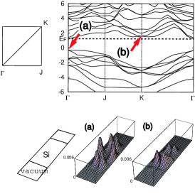
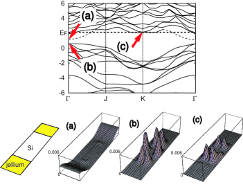
We first show the band structure and the (squared absolute value of) the wave functions obtained with LDA for , i.e., no jellium (Fig.3), (Fig.4) and (Fig.5), respectively. In the absence of the metal (), we can see that the valence band top is at , while the conduction band bottom lies around (and ). Hereafter, we focus on the energy shifts of the valence band top around and the conduction band bottom around caused by the close contact with the jellium.
When in vacuum the LDA band gap across and is 1.93 eV. When we introduce the jellium with or 4, the Fermi level still lies across and , i.e., only a small amount of electrons flow from the jellium into the Si side, so the effect of the charge rearrangement is almost completely absent. For smaller values of , on the other hand, we can show that electrons in the jellium do flow into the Si side, and the electronic band structure changes drastically. Thus we focus here on the case of and 4.
For , the band gap across and K reduces to 1.85 (1.79) eV. The characters of the wave functions at these points are mainly Si and do not change, as we can see in Fig.3, 4, and 5. In addition we notice that there is a state which emerges around crossing the Fermi level for (the bands represented by bold lines in the figures). If we examine the character of wave functions on these branches in Figs. 4,5, they reside well within the metallic side, so we exclude them from our argument on the band-gap narrowing in the semiconductor side.
B and the direct exchange term
Now we are in position to analyse the band gap reduction term by term. Here we consider and the direct exchange term , the energy independent part of the GW correction to the LDA eigenenergy. The expectation value of the exchange-correlation potential is obtained by . We have found that in the Si region has similar values for , 6 and 4. Since the characters of the wave functions do not change as we have seen in Figs.3, 4, and 5, we can expect that does not change significantly when we introduce the jellium between the Si system.
On the other hand, the value of the matrix elements between the metal wave functions and the semiconductor wave functions, , which governs , are small, since the states of jellium character and Si character are well separated in real space (see Figs.4,5). Therefore, we can expect that does not change significantly when we introduce the jellium.
In fact, at K is in eV for , so the shift is negligible. At , is in eV for .
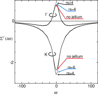
C Energy-dependent
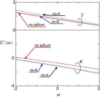
Finally, let us discuss the correlation contribution, . In Fig. 6, we show the imaginary frequency dependence of at and K.
We have then performed an analytic continuation onto the real energy axis with the Padé approximation[21]. In Fig.7, we show the real frequency dependence of . We can see that there is an almost linear dependence on .
When is linear for small , the GW correction to the LDA spectrum reduces to
where
From Fig.7, we can see that . At , is estimated to be in eV for . At K, is in eV. Thus the band-gap reduction due to the presence of the jellium amounts to as large as eV for and eV for .
V Discussions
To summarize, we have studied, with the GW approximation and a character-resolved band analysis, the image-potential band-gap narrowing at a metal/semiconductor interface by calculating quasi-particle energy spectrum of the jellium/Si interface. For the values of of jellium studied here the electrons or holes do not flow from the metallic to semiconducting side, i.e., the Fermi energy of the jellium lies within the energy gap of Si, so the one-body effect due to the charge redistribution is absent. We have found that a significant band gap narrowing of eV occurs for as large as .
So we can concentrate on the semiconducting side to realize larger gap-narrowing effects or a local metal-insulator transition. If the dielectric constant of the semiconductor is small, the image potential effect will become stronger, so that we may expect larger band gap narrowing. However, the system with a small dielectric function usually occurs in materials with large band gap, so that the realization of the band-gap closure becomes a trade-off. Furthermore, the energy gap of the semiconducting layer may depend on the surface structure (e.g., whether it is terminated by hydrogen atoms or dangling bonds form dimers, etc.), and their effect is also non-trivial. These are interesting future problems.
Finally, while the band gap narrowing or closure is of a fundamental interest in its own right, we can further raise a very strong motivation for considering a metallized semiconductor surface. There is a long history[22] of proposals for superconductivity in conducting systems in close contact with polarizable media. Little[23] proposed this for one-dimensional systems, then Ginzburg[24] extended this to two-dimensional systems. Allender, Brey and Bardeen[25] studied this in detail, with metal-semiconductor structures in mind, which was subsequently criticized by Inkson and Anderson[26]. A summary of the situation by Zharkov[22] is that, while the criticism is correct for the usual form for the dielectric function, the situation may be resurrected for unusual dielectric functions. The background to all this is that for the polarizable-medium mediated superconductivity, the conduction layer should be very strongly coupled to the semiconducting layer, ideally with strong chemical bonds such as covalent ones. So the metallized semiconductor surface, with the band-closure mechanism, should be one ideal realization of this.
VI Acknowledgment
One of the authors (KK) in indebted to Y. Murata for arousing his interests in the surface. HA wishes to thank J.C. Inkson for illuminating discussions. Thanks are also due to M. Tsukada, A. Koma and M. Kiguchi for discussions. The LDA calculation was performed with TAPP (Tokyo Ab-inito Program Package), where RA would like to thank S. Koizumi for technical advices. The numerical calculation was performed with SR8000 in ISSP, University of Tokyo. This work is in part funded by a Grant-in-Aid for Scientific Research from Ministry of Education of Japan.
REFERENCES
- [1] J.C. Inkson, Surf. Sci. 28, 69 (1971).
- [2] J.C. Inkson, J. Phys. C 4, 591 (1971).
- [3] J.C. Inkson, J. Phys. C 5, 2599 (1972).
- [4] J.C. Inkson, J. Phys. C 6, 1350 (1973).
- [5] P.W. Anderson in Elementary Excitation in Solids, Molecules and Atoms Part A, edited by J.A. Devreese, A.B. Kunz and T.C. Collins (Plenum, 1974), p.1.
- [6] Y. Murata et al., unpublished.
- [7] M. Kiguchi et al., unpublished.
- [8] A. Okiji and H. Kasai [Surf. Sci. 86, 529 (1979)] have theoretically studied the Mott gap closure at an interface in the Hubbard model.
- [9] J.P.A. Charlesworth, R.W. Godby and R.J. Needs, Phys. Rev. Lett. 70, 1685 (1993).
- [10] P. Hohenberg and W. Kohn, Phys. Rev. 140, A1133 (1965).
- [11] W.G. Aulbur, L. Jönsson and J.W. Wilkins in Solid State Physics Vol 54, edited by H. Ehrenreich, F. Seitz, and D. Turnbull (Academic Press, New York, 2000), p.1.
- [12] L. Hedin, Phys. Rev. 139, A796 (1969).
- [13] L. Hedin and S. Lundqvist in Solid State Physics Vol 23, edited by H. Ehrenreich, F. Seitz, and D. Turnbull (Academic Press, New York, 1969), p.1.
- [14] F. Aryasetiawan and O. Gunnarsson, Rep. Prog. Phys. 61, 237 (1998).
- [15] J. P. Perdew and Y. Wang, Phys. Rev. B 45, 13244 (1992)
- [16] N. Troullier and J.L. Martins, Phys. Rev. B 41, 7892 (1990).
- [17] J. Yamauchi, M. Tsukada, S. Watanabe and O. Sugino Phys. Rev. B 54, 5586 (1996).
- [18] H.N. Rojas, R.W. Godby and R.J. Needs, Phys. Rev. Lett. 74, 1827 (1995).
- [19] M.M. Rieger, L. Steinbeck, I.D. White, H.N. Rojas and R.W. Godby, Comp. Phys. Commun. 117, 211 (1999).
- [20] S. Baroni and R. Resta, Phys. Rev. B 33, 7017 (1986).
- [21] H. J. Vidberg and J.W. Serene, J. Low. Temp. Phys. 29, 179 (1977).
- [22] G.F. Zharkov in High-Temprature Superconductivity edited by V.L. Ginzburg and D.A. Kirzhnits, (New York Consultants Bureau, 1982).
- [23] W. A. Little, Phys. Rev. 134 1416 (1964).
- [24] V. L. Ginzburg, Zh. Eksp. Thor. Fiz. 46 397(1964)[Sov. Phys. JETP 19 269(1964)].
- [25] D. Allender, J.Bray and J. Bardeen, Phys. Rev. B 7, 1020(1973), 8, 4433 (1973).
- [26] J.C. Inkson and P.W. Anderson, Phys. Rev. B 8, 4429(1973).