On the Cooling of Electrons in a Silicon Inversion Layer
Abstract
Cooling of two-dimensional electrons in silicon-metal-oxide semiconductor field effect transistors is studied experimentally. Cooling to the lattice is found to be more effective than expected from the bulk electron-phonon coupling in silicon. The extracted heat transfer rate to phonons at low temperatures depends cubically on electron temperature, suggesting that another coupling mechanism (such as piezoelectric coupling, absent in bulk silicon) dominates over the deformation potential. According to our findings, at 100 mK, the electrons farther than m from the contacts are mostly cooled by phonons. Using long devices and low excitation voltage we measure electron resistivity down to electron temperature mK and find that some of the “metallic” curves, reported earlier, turn insulating below K. This finding renders the definition of the proposed 2D metal-insulator transition questionable. Previous low temperature measurements in silicon devices are analyzed and thumb rules for evaluating their electron temperatures are provided.
Since the scaling theory for non-interacting electrons was constructed in the late seventies[1], it was conjectured that a realistic two-dimensional electron system is insulating in the sense that its resistance diverges at low temperatures due to quantum interference and interaction effects. As the temperature is reduced, a logarithmic resistance increase due to weak localization is expected, followed by an exponential resistance divergence once strong localization commences[1]. It was later suggested[2] that strong Coulomb interaction may counteract localization and lead to the existence of a two dimensional metallic state and a metal-insulator transition at zero temperature.
Early experiments on various types of two dimensional electron gases (2DEG) supported localization. For a comprehensive review of early theoretical and experimental results see Refs. [3, 4]. It was therefore unexpected when the existence of a two dimensional metallic phase in high mobility silicon Metal Oxide Semiconductor Field Effect Transistors (MOSFET) was reported in 1994[5, 6]. The ultimate signature of such a metallic phase is resistance saturation to some residual value as the temperature approaches zero [7, 8]. Since is experimentally inaccessible, all claims for a metallic phase rely on extrapolation from finite temperatures. Two traps lurk an experimentalist in this procedure: (a) The assumption that the observed resistance saturation indeed persists to zero temperature may turn wrong. (b) The electron temperature may (and does indeed) depart from the lattice or bath temperature, , as . The latter point is particularly acute in silicon MOSFETs due to the high intrinsic contact resistance and the weak electron-phonon coupling.
The experiments described here focus on the second point. Using the sample itself as a thermometer we analyze electron cooling as a function of mixing chamber temperature and excitation voltage. The main findings are: (a) Electron cooling to the lattice is more effective than expected from the known bulk electron-phonon coupling in silicon. Power dissipation is given by with and and, hence, at temperatures below K, dominated by the term[9]. (b) Hot electron diffusion (ED) to the contacts is unimportant in large devices. In short Si MOSFETs, according to our estimates, ED provides cooling or heating depending on the contact resistance. (c) Comparing cooling by phonons with cooling by ED at e.g., 100 mK, we find the latter mechanism is typically important only for electrons closer than to the contacts. In longer devices, cooling proceeds through phonons. (d) Cooling the electrons down to 100 mK solely by phonons requires an excitation power estimated to be less than . For a 1 mm square of 2DEG with 30 K resistivity this figure implies an excitation voltage below . A square with the same resistance requires an excitation voltage below .
Four terminal, lock-in ac measurements at 11 Hz were carried out on samples similar to those used in Refs.[5, 6]. The samples were 5 mm long, 0.8 mm wide Hall bars with 2.5 mm separation between potential probes. The oxide thickness was 200 nm. Battery powered electrometer preamplifiers were employed to minimize electromagnetic interference and spurious offset bias across the potential probes. With 300pF cable capacitance, samples up to a few total resistance were measured with negligible “out of phase” signal. The excitation voltage across the whole sample was maintained below to guarantee tolerable heating (this figure is justified below). In order to reduce the contact resistance we applied a larger positive front gate voltage and substrate bias, thus maintaining the same carrier concentration range. The substrate bias depletes both the channel and the contacts, but it’s effect on the latter is smaller due to heavy doping in the contact regions. This way we were able to reduce the contact resistance below for all “metallic” densities. The substrate bias results in a moderate reduction of the peak mobility from e.g., at zero substrate bias to (both measured at K ). The mobility reduction is attributed to enhanced surface scattering due to shift of the 2DEG towards the interface. The substrate bias was changed in the presence of red LED illumination, which heats the crystal, thus facilitating acceptor recharging in the depletion layer. The high contact resistance problem is further complicated below 1.2K by superconductivity of the Al contact metallization. All our “zero magnetic field” measurements were, therefore, carried out in the presence of a 0.01 T parallel magnetic field which quenched the Al superconductivity.
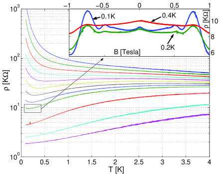
The resistivity vs bath temperature for a peak mobility sample at various densities is depicted in Fig. 1. For temperatures above 0.4 K the traces are similar to those reported in Refs. [5, 6]. At low densities the sample is insulating, while at higher densities the resistance decreases as the temperature is reduced, a behavior previously assigned to a two dimensional metal. For the resistance is practically independent of in a wide temperature range, K. Such a phenomenon was previously identified as a metal to insulator transition (MIT) [5, 6, 7]. Upon cooling the sample below 0.4K, we find a novel result; the resistance of some of the “metallic” curves turns upward, showing an insulating behavior in all three devices studied by us.
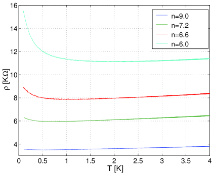
Measurements on a lower mobility sample with peak mobility (Fig. 2) at 0.3 K yield results similar to those reported earlier[8, 10] for the same type of samples. As the temperature decreases, the low mobility sample displays a pronounced insulating behavior at all measured densities, above . A relatively small resistivity drop with cooling is again followed by a resistivity increase at lower temperatures. Such curves have been observed earlier for 2D holes in Si-Ge [11], 2DEG on vicinal Si-surfaces [12], high mobility Si MOSFETs at higher densities, [13, 14], and in 2D systems on other materials [15, 16]. We attribute this resistance upturn to interference and Coulomb interaction effects that grow as the temperature is reduced. The interference is clearly manifested in the weak localization magnetoresistance curves depicted in the inset to Fig. 1.
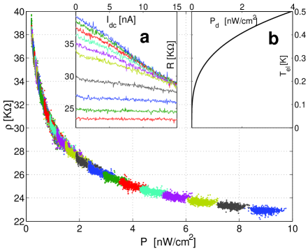
To gain insight into the electron cooling mechanisms we studied the resistivity dependence upon excitation. We applied a small ac signal superimposed on a dc bias and measured the differential resistivity as a function of this bias. The ac excitation was typically about 100 pA, generating less than ac voltage drop across the 5 mm sample. The analysis assumes the resistivity depends on the electronic temperature alone and uses the sample resistivity as a thermometer. We chose to use the low mobility sample due to its moderate resistance and monotonic temperature dependence, which facilitate accurate ac measurements.
Inset (a) to Fig. 3 depicts the channel resistivity versus dc current at various bath temperatures. The overall dissipated power per unit area of the 2DEG consists of Joule heating, , by the driven current and heating by spurious excitations, , due to e.g., absorption of electromagnetic radiation. The heat is dumped to phonons and to the contacts via electron diffusion. We ignore for the moment electron diffusion - an assumption to be later justified for our samples. In the general case, electron-phonon interaction may be due to both piezoelectric and deformation potential coupling with their characteristic and dependencies[17], respectively. Similar functional form was recently found for holes in SiGe heterostructures [18]. We therefore characterize the electron phonon interaction by the coupling parameters and .
| (1) |
We solve Eq. 1 to find the electron temperature, , and fit and in such a way that all data in inset (a) to Fig. 3 collapse to a single curve. Figure 3 shows the best fit obtained with and . cannot be determined in this scaling procedure. The piezoelectric contribution is, hence, found to dominate electron - phonon coupling at all temperatures below 0.6 K. This effect is unexpected since a Si lattice possesses inversion symmetry and, hence, should display deformation potential coupling only. We believe the piezoelectric contribution, found in our experiment, originates from the interface which lacks inversion symmetry.
Heat transfer due to ED can be incorporated into the model using the Wiedemann-Franz law [19]. The power balance reads
| (2) | |||
| (3) |
where is the sample conductivity. At temperatures the deformation potential contribution can be ignored. Defining and
| (4) |
Eq. 2 takes the dimensionless form
| (5) |
where and . sets the characteristic length scale on which the approaches . The only temperature scale in the problem is , the electron temperature far away from the contacts, where cooling is dominated by phonons. Equation 5 can be integrated exactly. Away from the contacts, where , . For , where is the normalized electron temperature near the contact.
For and (typical critical region conductance), . For our 5mm long samples, ED is, hence, negligible and Eq. 1 can be safely used to estimate . The resulting electron temperature as a function of dissipated power, is plotted in inset (b) to Fig. 3. Assuming that the electron-phonon coupling does not depend significantly on impurity scattering we use the same parameters to analyze the high mobility sample data. Equation 1 shows that the overheating due to the measurement current is negligible and does not exceed 1 mK for a 50 mK base temperature. We have used the magnetoresistance curves shown in the inset to Fig. 1 to estimate the lowest sample temperature by fitting the curves to weak localization theory. The extracted dephasing rate scales linearly with temperature, in agreement with theory[4], down to the lowest analyzed temperature, mK. Although we use weak localization theory for resistivities beyond its applicability, the linear dependence of the dephasing rate upon bath temperature indicates that electrons cool down to mK.
We turn now to investigate the implications of our results to previous measurements. Surprisingly, there are only a few published experiments below 300 mK. Those experiments were carried out on two types of samples. The first type, in which the MIT was originally observed [5, 6], is a conventional MOSFET that, in the lack of back gating, suffers from high contact resistance, especially at low electron densities and temperatures. These samples are several mm long, and heat transfer by electron diffusion to the contacts can be safely neglected. In the interesting regime, where the resistance drop is significant, the contact resistance is in the range. Such a high contact resistance dictates either dc or very low frequency measurements which require, due to noise in the amplifiers and the sample, substantial excitation currents. Overheating is evident in both vs and vs dependencies (see e.g., Figs. 1 and 5 in [6] and Fig. 3 of [20]), even in the insulating regime where it should be less significant. In previous experiments[21, 22], where was measured in the “metallic” regime, it was never lower than mK.
In another type of samples[23, 24], the gates, adjacent to the contacts, are separated from the gate over the central part of the sample by nm gaps. This arrangement facilitates a higher carrier concentration in the contact regions and, hence, a reduced contact resistance. In contrast to the millimeters long samples, employed here and in Refs. [5, 6], the effective sample length between the gaps in Ref. [24] is only . Substituting into Eq. 4 and solving for we find that cooling is mostly provided by phonons for all temperatures above mK. Since cooling by phonons is suppressed only slightly faster than by ED ( compared with ), phonons, neglected in the analysis of Ref. [24] done in Ref. [8], are important also at lower temperatures. Electron diffusion from the contacts may either cool or warm electrons in the central part of the sample, depending on the voltage drop, , across the nm gap. For a given electron temperature near the contact, , one can estimate the voltage drop, , across the gap resistance, , for which the net heat flow between the contact and the sample vanishes. Using Wiedemann-Franz law, the heat flow balance reads
| (6) |
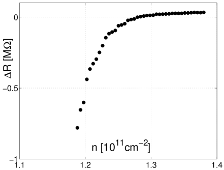
For one obtains , independent of . For lower (higher) voltages across , electrons are cooled (warmed) by the contacts. For 100 mK, the bias at which the contacts neither heat nor cool the sample equals 15.6 . At that bias sample cooling is provided by phonons. Using Eq. 1 we find that 100 mK electron temperature in a 30 per square sample requires less than voltage drop per m square, which for the sample in Ref. [24], translates into between the gate gaps. A 100 mK electron temperature throughout the sample thus requires less than V (50 mK requires V ) bias across the whole sample (neglecting the voltage drop across the high density contacts). Electron overheating in the contact regions occurs in our samples, as illustrated in Fig. 4. The contact regions are always more resistive than the rest of the sample in the “metallic” regime, , and less resistive in the insulating one, , indicating they are warmer than the rest of the sample.
In summary, we found that the cooling of electrons by phonons in Si MOSFETs is substantially more effective than that expected from the bulk electron-phonon coupling. Long samples are cooled by phonons. Short samples are susceptible to heat transfer by ED from the contacts. Low temperature measurements in short samples require low excitations. Using 5 mm long devices, where electron heating in the contacts can be neglected, we were able to measure electron resistivity down to mK temperatures. We found that -curves in the well pronounced “metallic” regime, corresponding to cm-2 densities and a three fold resistance reduction with cooling, turn insulating below a certain temperature. That temperature is mK at and decreases as the density is increased and decreases. Our finding renders the definition the 2D metallic phase and the metal-insulator phase transition questionable. Further work is needed to determine the physics behind the observed resistance upturn.
We have benefited greatly from valuable discussions with Y. Yaish, M. Gershenson, A. Finkelstein, A. Stern, and T. M. Klapwijk. This work was supported by the Israeli National Science foundation, the DIP foundation, INTAS, NSF, NATO Scientific Program, RFBR, and the Russian programs: “Physics of Nanostructures”, “Statistical Physics”, “Integration”, and “The State Support of Leading Scientific Schools”.
REFERENCES
- [1] E. A. Abrahams, P. W. Anderson, D. C. Licciardello, and T. V. Ramakrishnan, Phys. Rev. Lett.42 673 (1979).
- [2] A. M. Finkelstein, JETP 84, 168 (1983). Z. Phys. B 56, 189 (1984)
- [3] P. A. Lee, T. V. Ramakrishnan, Rev. Mod. Phys. 57, 287 (1985).
- [4] B. L. Altshuler and A. G. Aronov, in Electron-electron interactions in disordered systems, ed. by A. L. Efros and M. Pollak , p. 1 (Elsevier, Amsterdam, 1985).
- [5] S. V. Kravchenko, G. V. Kravchenko, J. E. Furneaux, V. M. Pudalov, M. D’Iorio, Phys. Rev. B 50, 8039 (1994), cond-mat/9405082.
- [6] S. V. Kravchenko, W. E. Mason, G. E. Bowker, J. E. Furneaux, V. M. Pudalov, M. D’Iorio, Phys. Rev. B 51, 7038 (1995), cond-mat/9412103.
- [7] E. Abrahams, S. V. Kravchenko, M. P. Sarachik, Rev. Mod. Phys. 73, 251 (2001), cond-mat/0006055.
- [8] B. L. Altshuler, D. L. Maslov, and V. M. Pudalov, Physica E, 9, 209 (2001), cond-mat/0003032.
- [9] This form is equivalent to the empirical law, over the range K.
- [10] V. M. Pudalov, G. Brunthaler, A. Prinz, G. Bauer, Physica E 3, 79 (1998).
- [11] V. Senz, T. Heinzel, T. Ihn, K. Ensslin, G. Dehlinger, D. Grützmacher, and U. Gennsher, Phys.Rev.B 61, 5082 (2000), cond-mat/9910228.
- [12] S. S. Safonov, S. H. Roshko, A. K. Savchenko, A. G. Pogosov, Z. D. Kvon, Phys. Rev. Lett. 86, 272 (2001), cond-mat/0003060.
- [13] V. M. Pudalov, G. Brunthaler, A. Prinz, and G. Bauer, Phys. Rev. B 60, 2154 (1999), cond-mat/9801077.
- [14] B. L. Altshuler, G. W. Martin, D. L. Maslov, V. M. Pudalov, A. Prinz, G. Brunthaler, G. Bauer, cond-mat/0008005.
- [15] Y. Y. Proskuryakov, A. K. Savchenko, S. S. Safonov, M. Pepper, M. Y. Simmons, D. A. Ritchie, Phys. Rev. Lett. 86, 4895 (2001), cond-mat/0101195.
- [16] E. Ribeiro, R. Jaäggi, T. Heinzel, K. Ensslin, G. Medeiros-Ribeiro, and P. M. Petroff, Phys. Rev. Lett., 82, 996 (1999), cond-mat/9808276.
- [17] V. Karpus, Semic. Sci. Technol. 5, 691 (1990).
- [18] R. Leturcq, D. L’Hote, R. Tourbot, V. Senz, U. Gennser, T. Ihn, K. Ensslin, G. Dehlinger, D. Gr?tzmacher, cond-mat/0107457.
- [19] Wiedemann-Franz law remains valid in Fermi-liquid in presence of interactions (see M. Reizer, Phys. Rev. B 44, 12701 (1991)).
- [20] M. D’Iorio, V. M. Pudalov, and S. G. Semenchinsky, Phys. Rev. B 46, 15992 (1992).
- [21] G. Brunthaler, A. Prinz, G. Bauer, and V. M. Pudalov, cond-mat/0007230. PRL (2001), in press.
- [22] V. M. Pudalov, M. Gershenson, H. Kojima, N. Butch, E. M. Dizhur, G. Brunthaler, A. Prinz, G. Bauer, cond-mat/0105081. M. Gershenson et al., in the EP2DS-14 workbook, Prague (2001).
- [23] R. Heemskerk, “Transport at Low Electron Densitity in the Two-Dimensional Electron Gas of Silicon MOSFETs” PhD Thesis, Rijksuniversiteit Groningen (1998), adviser: T. M. Klapwijk.
- [24] S. V. Kravchenko and T. M. Klapwijk, Phys. Rev. Lett. 84, 2909 (2000), cond-mat/9909458.