Observation of Andreev reflection in the -axis transport of Bi2Sr2CaCu2O8+x single crystals near and search for the preformed-pair state
Abstract
We observed an enhancement of the -axis differential conductance around the zero-bias in AuBi2Sr2CaCu2O8+x (Bi2212) junctions near the superconducting transition temperature . We attribute the conductance enhancement to the Andreev reflection between the surface Cu-O bilayer with suppressed superconductivity and the neighboring superconducting inner bilayer. The continuous evolution from depression to an enhancement of the zero-bias differential conductance, as the temperature approaches from below, points to weakening of the barrier strength of the non-superconducting layer between adjacent Cu-O bilayers. We observed that the conductance enhancement persisted up to a few degrees above in junctions prepared on slightly overdoped Bi2212 crystals. However, no conductance enhancement was observed above in underdoped crystals, although recently proposed theoretical consideration suggests an even wider temperature range of enhanced zero-bias conductance. This seems to provide negative perspective to the existence of the phase-incoherent preformed pairs in the pseudogap state.
pacs:
73.40.-c, 74.50.+r, 74.72.Hs, 74.80.FpI Introduction
It is now widely accepted that the dominant order parameter (OP) of high- superconductors (HTSC’s) has a -wave (-wave) symmetry,DJ ; twin ; Ng ; Wei along with other minor components.twin ; Covington ; Mossle The existence of nodes and the azimuthal phase alternation of the -wave OP in the superconducting Cu-O bilayers leads to novel phenomena in the electrical transport such as the formation of -junctions DJ ; twin ; Schulz and zero-bias conductance peak.Ng ; Wei ; Tanaka In general, the zero-bias conductance peak is observed in normal-metalHTSC junctions with the tunneling direction along the plane of a Cu-O bilayer. It results from a coherent interference of incident and reflected quasiparticles with energies lower than the superconducting gap of a HTSC electrode near the junction interface. The coherent state in the -wave superconductor, which is called the Andreev bound state (ABS), occurs when the quasiparticles in the Cu-O bilayer experience sign changes of OP upon reflection at the interface. Thus, the ABS effect is more pronounced for a junction which is normal to one of the node directions of the -wave OP. A resonant tunneling of quasiparticles in the normal-metal electrode to the ABS of the HTSC crystal leads to the zero-bias conductance peak. In contrast to the conventional Andreev reflection (AR) effect,Andreev ; BTK where maximum zero-bias conductance enhancement is obtained for negligible interfacial barrier strength, a finite scattering barrier at the interface is essential for the observation of the zero-bias conductance peak through the ABS.Tanaka
The -axis electrical transport properties of the HTSC’s can be well understood in terms of -axis stacking of intrinsic Josephson junctions (IJJ’s), where the Cu-O bilayers serve as thin superconducting electrodes and the layers in-between as insulating layers. The -axis tunneling current-voltage characteristics (IVC) of the HTSC’s such as Bi2Sr2CaCu2O8+x (Bi2212) exhibit the features of stacked DID (-wave-HTSC/insulator/-wave-HTSC) IJJ’s at temperatures well below the superconducting transition temperature .IJJ However, the insulating layer acts as a strong interfacial scattering barrier and thus hinders the observation of a conventional AR along the -axis direction in HTSC junctions. Moreover, the quasiparticles which are reflected from the transverse boundary of Cu-O bilayers experience no sign change and thus the observation of the zero-bias conductance peak by the formation of the ABS in the -axis tunneling cannot be expected.Tanaka In this study, we report observation of the conventional AR in Bi2212 single crystals for the -axis transport at temperatures very close to the bulk superconducting transition temperature . In our previous work,Kim it has been shown that the superconductivity of the surface Cu-O bilayer in a Bi2212 single crystal is suppressed when the surface layer is in contact with a normal-metal electrode. Such suppression leads to the formation of a natural NID junction at the crystal surface, the “surface junction”, in the temperature range , where and are the transition temperatures of the surface and inner Cu-O bilayers, respectively. In this surface NID junction, N represents the surface Cu-O bilayer with suppressed superconductivity and the normal-metallic Au electrode, I is the non-superconducting layers between adjacent Cu-O bilayers, and D is the neighboring inner superconducting Cu-O bilayers with -wave OP symmetry. As the temperature is raised and approaches , the differential conductance near the zero-bias voltage of the surface junction develops from tunneling-like depression to an AR-like enhancement in a continuous manner. Such development points to gradual weakening of the barrier strength between adjacent Cu-O bilayers with increasing temperature. We show that the transitional feature can be confirmed numerically, at least in a qualitative level, using the formalism by Blonder, Tinkham, and Klapwidjk (BTK) for -wave symmetry.Tanaka
Recently, it has been proposed by Choi, Bang, and Campbell Choi that, if the pseudogap state above in the HTSC’s is described in terms of the phase-incoherent preformed pairs,Emery the AR can take place from such preformed pairs. They suggest that experimental observation of the resulting conductance enhancement in an -planar normal-metal/HTSC junction would provide unambiguous confirmation of the preformed pairs in the pseudogap state. Along with the suggestion of Ref. 13, we utilized the appearance of the AR effect along the c-axis direction near to investigate the existence of the preformed pairs in the pseudogap state. We observed the zero-bias conductance enhancement (ZBCE) in junctions prepared on the surface of as-grown overdoped Bi2212 single crystals over a-couple-of-degrees temperature window even above . However, no appreciable ZBCE has been observed above in underdoped crystals, although theoretical consideration of Ref. 13 suggests an even wider temperature window of ZBCE. Our result is consistent with the recent observation of the nonexistence of the AR effect in ab-planar normal-metal/HTSC junctions by Dagan et al. Dagan and seems to provide negative perspective to the existence of the preformed pairs in the pseudogap state.
II Experiment
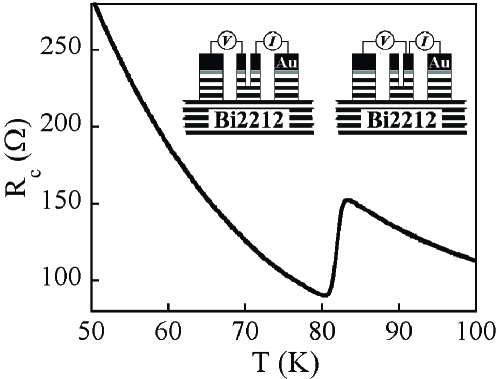
In this study, we used Bi2212 single crystals of different doping levels. As-grown overdoped crystals were prepared by the conventional solid-state-reaction method. Crystals in the underdoped level were grown first by traveling solvent floating zone methods. Reducing doping level was done by annealing the crystals in a low-concentration (0.1) oxygen gas mixed with nitrogen gas. The superconducting transition temperatures of the as-grown overdoped and underdoped crystals used were about 90 K and 83 K, respectively. For mesa fabrication, a-few-thousand-Å-thick Au film was deposited first on the surface of a freshly cleaved single crystal. Mesa structure was then formed by photolithographic micropatterning and ion-beam etching. Additional process of photolithographic patterning, metal deposition, and lift-off was done to attach contact leads to the small mesa area. Details of the mesa fabrication are described elsewhere.Kim ; Kim2 Finally, the central mesa (refer to the insets of Fig. 1) of typical lateral dimension of 1045 m2 was divided into equal halves by further etching it with the contact leads as masks. The dimension of each smaller mesa thus prepared in the central mesa was 1013 m2. We adopted the configurations in the left and right insets of Fig. 1 for the four- and three-terminal measurements, which were used to probe the lower and upper stacks of intrinsic junctions in the central mesa, respectively. The four-terminal configuration was used to monitor the intrinsic properties of the junctions, while the three-terminal configuration prepared on the same crystal was used to monitor the properties including the surface junction. The total thickness of the central mesa was usually less than 200 Å and the upper stack contained about 5-6 intrinsic junctions. The temperature dependence of the -axis resistance and the differential conductance were obtained by standard ac lock-in technique.
III Results and Discussion
Fig. 1 shows the typical -axis tunneling resistance of a mesa (UD2) fabricated on the surface of an underdoped Bi2212 single crystal in a three-terminal configuration. The bulk transition temperature should be close to the temperature of maximum curve, that is 82.5 K. As Kim et al. reported earlier Kim the superconductivity of the surface Cu-O bilayer of a Bi2212 single crystal, which is in contact with normal-metallic Au electrode, is significantly suppressed. The resulting formation of the surface NID junction is apparent as illustrated in Fig. 1 by the strongly semiconducting temperature dependence of the curve below . For the mesa UD2 in the underdoped regime the superconducting transition of the surface Cu-O bilayer was not observed down to 4.2 K, which was in contrast to previous observations in slightly overdoped crystals,Kim ; Kim2 ; Doh1 where the surface bilayers usually showed the superconducting transition at K. We believe that, in the case of underdoped crystals, the reduced hole doping of the surface Cu-O bilayer pTc ; Mossle2 contributes to the suppression of the superconductivity in addition to the proximity-induced suppression.
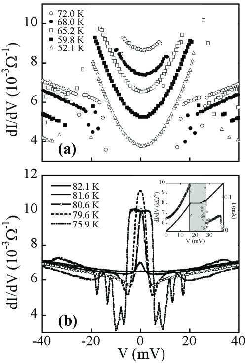
A set of differential conductances () of the mesa UD2 for various temperatures are shown in Fig. 2. The conductance was measured in the first branch of the IVC, which was from the surface junction of the mesa. The curves at the lower temperature range in Fig. 2(a) display distinct gap-like features. An intrinsic Josephson junction in the supercurrent branch of its IVC usually switches prematurely to the quasiparticle branch before the bias voltage reaches the gap edge. The sudden jumps of the differential conductance at finite voltages in Fig. 2(a) were caused by this premature switching, where the Josephson coupling of the inner junctions broke down before the gap edge of the inner Cu-O bilayer in the surface NID junction was reached. More details of the situation are illustrated in the inset of Fig. 2(b) for 65.2 K, where the IVC for biases below 16.5 mV and above 27 mV represent the first and the second quasiparticle branches, respectively. The shaded area in-between approximately marks the region of the voltage jump in the IVC. As the temperature is raised the depression of the differential conductance near the zero bias becomes shallower (Fig. 2(a)), and the conductance gradually exhibits an zero-bias enhancement (Fig. 2(b)) between 75.9 K and 79.6 K for this mesa. However, as shown in Fig. 2(b), in the middle of the superconducting transition slightly above 79.6 K, the magnitude of the zero-bias peak decreases with increasing temperature and finally vanishes near . The oscillations of the curve with rather regular periodicity at 75.9 K are believed to be caused either by the fluctuating Josephson coupling in the inner junctions underneath the surface junction near or by the coherent interference of boundary-reflected quasiparticles in the normal-metal electrode of the surface junction.Rowell ; Nesher
The appearance of the zero-bias enhancement of the differential conductance of this c-axis tunneling at temperatures just below is very surprising. It is in clear contrast to most of earlier results of -axis tunneling measurements in HTSC’s,Wei ; cat1 ; cat2 ; Miya1 ; Miya2 where at all temperatures explored, even very close to , only gap-like features have been observed. A very few cases of conductance enhancement in the -axis transport were reported Ng ; Ishibashi but with much less pronounced peaks than those observed in this study, so that earlier observation of the c-axis ZBCE was accounted for by leakage ab-plane tunneling through some surface defects.
The transition from gap-like depression to enhancement of the differential conductance was observed earlier in STM measurements on conventional superconductors.Sri ; Chuang By reducing the spacing between the normal STM tip and the superconductor surface the conduction characteristics of the system turned from tunneling-like to a weak-link behavior until the direct contact was made between the STM tip and the superconductor surface. The barrier strength parameter decreased correspondingly, along with the decrease of the tunneling resistance. Also, in a junction of AuBi2Sr2CuO6(Bi2201)Bi2212 single crystal, which was fabricated by sequential deposition of Bi2201 and Au films on a Bi2212 single crystal, Matsumoto et al. SAR observed excess zero-bias conductance with the temperature approaching from below. It was argued that the observed excess zero-bias conductance was caused by the conventional AR effect, where the effective value was reduced with increasing temperature by the semiconducting temperature dependence of the Bi2201 film. We suppose that the conventional AR effect with decreasing effective value slightly below was also responsible for the observed ZBCE in our measurements. One should note, however, that the increase of the resistance below in Fig. 1 was caused mainly by the temperature dependence of in Eq. (3) in the zero-bias limit, . Thus, the additional weak temperature dependence of should be determined from a careful fitting as described below. The possibility of an AR between Au layer and surface Cu-O bilayer can be ruled out, since the latter is non-superconducting at all temperatures under consideration. We assume that the reason for the scarcity of observation of the ZBCE in the -axis transport measurements of HTSC’s except for the cases of Refs. 3 and 26 was mainly because most of the previous measurements were focused on the temperature range sufficiently lower than with resultant strong barrier potential.
In order to confirm the possible appearance of the AR effect in the -directional conduction we followed the extended BTK formalism by Tanaka and Kashiwaya.Tanaka The BTK kernel for -wave HTSC’s in the case of pure -axis tunneling without any planar momentum components is given by
| (1) |
where . To account for the -wave OP of Bi2212 was chosen with as the azimuthal angle in the Cu-O layer.Won For the temperature dependence of OP magnitude of the underdoped crystal used the following empirical approximation gapftn was adopted.
| (2) |
The above expression for the gap of the underdoped Bi2212 crystal was obtained by fitting the temperature dependence of the gap used in Ref. 31 to the data in Ref. 25 for underdoped Bi2212 crystals with =83 K, where we used Oda 40 meV as the maximum value of the OP at zero temperature. Equation (2) agrees very well with the numerical solution of the BCS gap function except near , where underdoped samples are known to render a larger gap.Miya1 ; Miya2 Using these parameters the normalized conductance was calculated according to the BTK formula BTK as
| (3) |
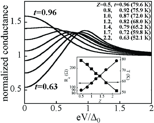
where is the Fermi distribution function. The values of the barrier strength parameter at different temperatures were chosen by fixing the calculated conductance of Eq. (3) for =0 to the measured differential conductance in Fig. 2. As shown in the inset of Fig. 3 the values of determined in this way are proportional to the logarithm of , which is consistent with earlier observations.Chuang In addition, the temperature dependence of agrees with the scenario of gradually weakening barrier strength with increasing temperature. Figure 3 displays the results of Eq. (3) corresponding to the curves of Fig. (2) for =52.179.6 K. The overall qualitative features of the calculated normalized conductance curves have almost one to one correspondence to the experimental data. At low temperatures, where the value is supposed to be relatively large, the calculated curves show gap-like features which are qualitatively similar to the observed ones. With increasing temperature the barrier strength parameter decreases and both the calculated and experimental conductance curves develop an AR-like enhancement near the zero-bias voltage in a continuous manner. The most pronounced discrepancy between the two sets of curves, however, is the width of the AR enhancement at higher temperatures; the measured widths are significantly narrower than the calculated ones. The discrepancy was caused mainly by the above-mentioned premature switching of a junction state to the quasiparticle branch; the switching took place before the voltage reached the gap edge and thus the width of the conductance enhancement was made narrower. Other possibilities are the decrease of the AR process itself due to thermal excitation of sub-gap-energy particles to the state above the gap and the thermal smearing of the gap edge at temperatures very close to . Both effects may decrease the effective OP magnitude experienced by the quasiparticles to a value smaller than that of Eq. (2).
We also observed similar gradual reduction of the barrier potential in a mesa (OD1) fabricated on an as-grown overdoped crystal (data are not shown). At temperatures sufficiently below ( 89 K) the IVC exhibited typical quasiparticle branches with high hysteresis. Thus, in the low temperature range, intrinsic junctions behaved as tunneling junctions with a high barrier potential. Approaching , however, the hysteresis gradually disappeared and the IVC became more or less SNS-junction like. This strongly suggests that the intrinsic junctions near may satisfy the clean interface condition and one may be able to observe the ZBCE by the AR in the c-axis conduction measurements.
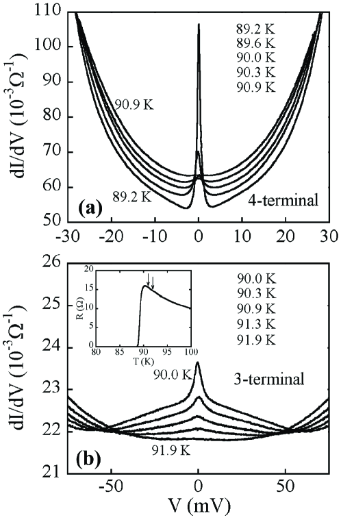
Taking the presence of -axis AR for granted near , we carefully investigated the existence of the -axis ZBCE above of mesas fabricated on single crystals of varied doping levels. The inset of Fig. 4(b) shows the resistive transition of another overdoped mesa OD3, taken in a four-terminal configuration. The mesa contained only several IJJ’s. The superconducting transition is relatively sharp and the temperature of maximum , which should be close to ,Tc is about 90.3 K. Since measurements in a four-terminal configuration do not include the surface effect, does not exhibit a finite resistance below as in Fig. 1. Thus, the inset of Fig. 4(b) illustrates the intrinsic transition properties of the inner junctions. As will be described below, the two arrows denote the temperatures above which the ZBCE in the four- (left arrow) and three-terminal (right arrow) configurations disappears.
Fig. 4(a) illustrates the differential conductance measured in the four-terminal configuration at temperatures very close to . The zero-bias peak at each temperature was caused by the Josephson pair tunneling over the stacked intrinsic junctions. With slightly increasing temperature the conductance peak reduces rapidly and disappears completely at 90.9 K, which is defined as the intrinsic value of of the crystal. We notice that the value of turns out to be slightly higher than the temperature of maximum . The concave background conductance represents the existence of the pseudogap in this temperature range.Parker The conductance data measured in a three-terminal configuration from the same central mesa are shown in Fig. 4(b). One should note that in this case the properties of the junctions in one of the smaller mesas including the surface junction were measured. At 90.9 K, where the pair-tunneling zero-bias conductance peak completely vanishes in the corresponding four-terminal measurements, a clear ZBCE still persists, although its magnitude is much smaller than the four-terminal counterpart. With increasing temperature the ZBCE gradually reduces and disappears completely only around 91.9 K. Thus, in this three-terminal configuration, one has a 1-K temperature window of ZBCE above the measured by the four-terminal configuration. In a different mesa (OD2) fabricated on another overdoped crystal, a 2-K temperature window of ZBCE above was obtained (data not shown). We believe that the ZBCE was caused by an AR in the surface junction between the normal electrode consisting of the Au film and the surface Cu-O bilayer with suppressed superconductivity, and the ”superconducting” electrode of the first inner Cu-O bilayer. Since the inner Cu-O bilayer is no more superconducting above 90.9 K, the AR effect in Fig. 4(b) is either from the thermally fluctuating superconducting order fluct or from the proposed preformed pairs in the pseudogap state. Then the significantly reduced magnitude of the ZBCE in the three-terminal configuration in Fig. 4(b) compared to the one in the four-terminal configuration in Fig. 4(a) is easily explicable, because both the thermally fluctuating pairs and the preformed pairs in the pseudogap region are in phase-incoherent states.
If the AR was genuinely from the preformed pairs as suggested by Ref. 13, the temperature window of the three-terminal ZBCE above should get wider for underdoped crystals. In the three-terminal configuration in Fig. 2, the ZBCE in the mesa of UD2 disappeared at 82.1 K, which was in fact even lower than the transition temperature (=83.5 K) determined from the four-terminal conductance measurements (not shown) on the same crystal. We suppose that this unphysical behavior obtained in UD2 was caused by the possible doping inhomogeneity along the depth of the mesa (lower doping near the surface of crystals), which was introduced during the annealing process of lowering the doping level. Due to this doping inhomogeneity the larger lower mesa probed by the four-terminal configuration may have shown even higher temperature of disappearing ZBCE than the upper mesa probed by three-terminal configuration. No doping inhomogeneity is supposed to develop in as-grown overdoped crystals. Since in UD2 the top Cu-O bilayer of the lower mesa was located only six layers below the surface Cu-O bilayer,inhomogeneity however, the effect of doping inhomogeneity should have been marginal. Thus the lack of the conductance enhancement in this underdoped crystal in the three-terminal configuration cannot be explained by the doping inhomogeneity only. We conclude that, contrary to the theoretical expectation, we have observed no appreciable ZBCE above in the underdoped crystal in the three-terminal configuration.
The great advantage of this measurement technique is in the fact the three- and four-terminal configuraions were prepared on the same ”central” mesa in an identical piece of single crystal. This geometry enabled us to determine the temperature, , where the pair tunneling ceases to exist in a four-terminal configuration. Then a delicate change of the temperature near in the three-terminal configuration, where the ZBCE due to the possible AR from phase-incoherent Cooper pairs starts disappearing, can be monitored very accurately.
In summary, we report that an AR has been observed in AuBi2212 single crystal junctions with the transport current along the axis of the Bi-2212 HTSC’s, in both underdoped and overdoped states. The features of the differential conductance curves changed from gap-like depression at low temperatures to an AR-like enhancement near . We attribute such continuous evolution to the AR between the proximity-suppressed surface Cu-O bilayer and the superconducting inner one as the barrier potential decreases with the temperature approaching from below. We utilized this appearance of the AR effect near to investigate the existence of the preformed pairs in the psudogap state above . In as-grown overdoped mesas we have observed maximally a 2-K temperature range where the three-terminal measurements exhibit the AR-induced ZBCE above which was determined in a four-terminal configuration. On the other hand, no appreciable ZBCE above has been detected in single crystals which were deep in the underdoped state, although theoretical consideration suggests a wider temperature range of ZBCE above . In the light of the results from underdoped crystals the ZBCE itself above in overdoped crystals may have been the thermal fluctuation effect of the superconducting order. If that is the case we have observed in this work no ZBCE by the AR from preformed pairs in the pseudogap state. Our results then agree with the recent report Dagan which negates the AR effect in -planar junctions by the preformed pairs in the pseudogap state but are in disaccordance with the observation of thermoelectrically induced vortices Nernst in a wide temperature range above in underdoped La2-xSrxCuO4. We believe that, more rigorous examination is also required on the validity of the suggested observationChoi of the AR effect from phase-incoherent preformed pairs.
Acknowledgements
One of us (H.-J. Lee) appreciates helpful private communications with Y. Bang and H.-Y. Choi, and Y. Bang’s critical reading of the manuscript. Useful discussion with Y.-J. Doh is also appreciated. The underdoped single crystals were provided by N. Momono and M. Ido in Hokkaido University. This work was supported by Korea Research Foundation, the center for excellency (SRC) administered by Korea Science and Engineering Foundation, and Basic Science Research Institute in POSTECH.
References
- (1) D. J. Van Harlingen, Rev. Mod. Phys. 67, 515 (1995).
- (2) K. A. Kouznetsov, A. G. Sun, B. Chen, A. S. Katz, S. R. Bahcall, John Clarke, R. C. Dynes, D. A. Gajewski, S. H. Han, M. B. Maple, J. Giapintzakis, J.-T. Kim, and D. M. Ginsberg, Phys. Rev. Lett. 79, 3050 (1997).
- (3) S. Sinha and K.-W. Ng, Phys. Rev. Lett. 80, 1296 (1998).
- (4) J. Y. T. Wei, N.-C. Yeh, D. F. Garrigus, and M. Strasik, Phys. Rev. Lett. 81, 2542 (1998).
- (5) M. Covington, M. Aprili, E. Paraoanu, L. H. Greene, F. Xu, J. Zhu, and C. A. Mirkin, Phys. Rev. Lett. 79, 277 (1997).
- (6) M. Mößle and R. Kleiner, Phys. Rev. B 59, 4486 (1999).
- (7) R. R. Schulz, B. Chesca, B. Goetz, C. W. Schneider, A. Schmehl, H. Bielefeldt, H. Hilgenkamp, J. Mannhart, and C. C. Tsuei, Appl. Phys. Lett. 76, 912 (2000); R. R. Schulz, B. Chesca, B. Goetz, C. W. Schneider, A. Schmehl, H. Bielefeldt, H. Hilgenkamp, J. Mannhart, and C. C. Tsuei, Physica C 341-348, 1651 (2000).
- (8) Y. Tanaka and S. Kashiwaya, Phys. Rev. Lett. 74, 3451 (1995).
- (9) A. F. Andreev, Sov. Phys. JETP 19, 1228 (1964).
- (10) G. E. Blonder, M. Tinkham, and T. M. Klapwijk, Phys. Rev. B 25, 4515 (1982).
- (11) R. Kleiner and P. Müller, Phys. Rev. B 49, 1327 (1994); A. Yurgens, D. Winkler, N. V. Zavaritsky, and T. Claeson, Phys. Rev. B 53, R8887 (1996).
- (12) N. Kim, Y.-J. Doh, H.-S. Chang, and H.-J. Lee, Phys. Rev. B 59, 14639 (1999).
- (13) H.-Y. Choi, Y. Bang, D. K. Campbell, Phys. Rev. B 61, 9748 (2000).
- (14) V.J. Emery and S.A. Kivelson, Nature 374, 434 (1995) and the references therein.
- (15) Y. Dagan, A. Kohen, G. Deutscher, and A. Revcolevschi, Phys. Rev. B 61, 7012 (2000).
- (16) N. Kim, Y.-J. Doh, H.-S. Chang, and H.-J. Lee, Physica C 341-348, 1563 (2000).
- (17) Y.-J. Doh, H.-J. Lee, and H.-S. Chang, Phys. Rev. B 61, 3620 (2000).
- (18) M. R. Presland, J. L. Tallon, R. G. Buckley, R. S. Liu, and N. E. Flower, Physica C 176, 95 (1991); G. V. M. Williams, J. L. Tallon, R. Michalak, and R. Dupree, Phys. Rev. B 54, R6909 (1996).
- (19) M. Mößle, R. Kleiner, R. Gatt, M. Onellion, and P. Müller, Physica C 341-348, 1571 (2000).
- (20) J. M. Rowell and W. L. McMillan, Phys. Rev. Lett. 16, 453 (1966).
- (21) O. Nesher and G. Koren, Phys. Rev. B 60, 9287 (1999).
- (22) S. Matsuo, M. Suzuki, X. G. Zheng and S. Tanaka, Physica C 282-287, 1497 (1997); H. J. Tao, F. Lu, and E. L. Wolf, ibid. 282-287 1507 (1997).
- (23) Ch. Renner, B. Revaz, J.-Y. Genoud, K. Kadowaki, and Ø. Fischer, Phys. Rev. Lett. 80, 149 (1998); Y. DeWilde, N. Miyakawa, P. Guptasarma, M. Iavarone, L. Ozyuzer, J. F. Zasadzinski, P. Romano, D. G. Hinks, C. Kendziora, G. W. Crabtree, and K. E. Gray, ibid. 80, 153 (1998); L. Ozyuzer, Z. Yusof, J. F. Zasadzinski, R. Mogilevsky, D. G. Hinks, and K. E. Gray, Phys. Rev. B 57, R3245 (1998).
- (24) N. Miyakawa, J. F. Zasadzinski, L. Ozyuzer, P. Guptasarma, D. G. Hinks, C. Kendziora, and K. E. Gray, Phys. Rev. Lett. 83, 1018 (1999).
- (25) N. Miyakawa J. F. Zasadzinski, L. Ozyuzer, P. Guptasarma, C. Kendziora, T. Kaneko, D. G. Hinks, and K. E. Gray, Physica C 341-348, 835 (2000).
- (26) T. Ishibashi, K. Sato, and K. Sato, Physica C 341-348, 1615 (2000).
- (27) H. Srikanth and A. K. Raychaudhuri, Phys. Rev. B 45, 383 (1992).
- (28) C. H. Chuang and T. T. Chen, Physica C 265, 89 (1996).
- (29) T. Matsumoto, S. Choopun, and T. Kawai, Phys. Rev. B 52, 591 (1995); see also N. Tsuda, T. Arao, T. Hosokawa, Y. Shiina, N. Matsuda, and D. Shimada, Physica C 282-287, 1489 (1997).
- (30) H. Won and K. Maki, Phys. Rev. B 49, 1397 (1994).
- (31) J. H. Xu, J. L. Shen, J. H. Miller, Jr., and C. S. Ting, Phys. Rev. Lett. 73, 2492 (1994).
- (32) M. Oda, T. Matsuzaki, and M. Ido, Physica C 341-348, 847 (2000).
- (33) The accurate value of should be obtained by the disappearing temperature of the differential conductance in the four-terminal measurements. In the resistive transition, however, the can be at best loosely defined.
- (34) I. F. G. Parker, C. E. Gough, M. Endres, P. J. Thomas, G. Yang, and A. Yurgens, Proc. SPIE, 3480, 11 (1998).
- (35) The AR effect from the thermally fluctuating superconducting order should be weaker than from the preformed pairs, if there is any, since the preformed-pair state is represented by phase fluctuations only while the thermally fluctuating state is subject to fluctuations both in the amplitude and the phase of the superconducting order (Refer to Q. Chen, I. Kosztin, B. Janko, and K. Levin, Phys. Rev. Lett. 81, 4708 (1998); Y. Yanase and K. Yamada, J. Phys. Soc. Jpn. 70, 3664 (2000)).
- (36) The number of Cu-O bilayers in one of the upper mesas was identified by counting the number of quasiparticle branches in its hyteretic IVC at temperatures sufficiently below .
- (37) Z. A. Xu, N. P. Ong, Y. Wang, T. Kakeshita, S. Uchida, Nature 406, 486 (2000).