The controllable - SQUID
Abstract
We have fabricated and studied a new kind of DC SQUID in which the magnitude and sign of the critical current of the individual Josephson junctions can be controlled by additional voltage probes connected to the junctions. We show that the amplitude of the voltage oscillations of the SQUID as a function of the applied magnetic field can be tuned and that the phase of the oscillations can be switched between 0 and in the temperature range of 0.1 - 4.2 K using a suitable control voltage. This is equivalent to the external application of (n+1/2) flux quantum.
The direct current superconducting quantum interference device (DC SQUID) is the most sensitive magnetic flux sensor currently available. It combines two phenomena: Flux(oid) quantization and the Josephson effect [1, 2, 3]. The critical current of the SQUID is an oscillatory function of the applied magnetic flux with a period given by the flux quantum Wb. Using a suitable current a little larger than the sum of the critical currents of the 2 Josephson junctions the oscillating critical current is transformed into an oscillatory voltage. The SQUID can be designed to meet various demands. However, once fabricated, the properties of the device, in particular the critical currents of the two Josephson junctions, are fixed. On the other hand, a recent development in the field of mesoscopic superconductivity is the controllable Josepshon junction. In such a junction it is possible to change the magnitude of the critical current [4, 5, 6] and even reverse its direction with respect to the phase difference between the superconducting electrodes [7, 8, 9, 10, 11, 12]. This corresponds to an extra phase factor of in the Josephson supercurrent () - phase relation . This -junction behaviour is well known in the field of high Tc superconductors [13] and has also been observed in ferromagnetic weak links [14]. However, the state (normal or ) of the junction is fixed once the device has been made, this in contrast with a controllable -junction. We have implemented such a controllable Josephson junction in a DC SQUID, which leads to a controllable -SQUID, in which the critical currents of the individual junctions [15] and hence the symmetry of the SQUID can be fine tuned. More interestingly the device can be switched from a state where no circulating current is running around the SQUID loop (at =n with n an integer), to a state with a circulating current running around the SQUID loop, without the application of an external magnetic field, but by switching one of the weak links into the -state. This is a consequence of the condition of a single-valued wave function around the SQUID loop:
| (1) |
where the total flux , the flux due to the screening current. Switching for example junction 1 in the -state changes with , which leads to the same solution of the equation if the junction would be in the normal state and .
In this Letter we propose and demonstrate experimentally the controllable -SQUID and show that the magnitude of the voltage oscillations as a function of the applied magnetic field (V-B oscillations) can be tuned and shifted a factor of in phase.
The only realization so far of a controllable -junction is based upon a superconductor - normal metal - superconductor junction in which the normal region is made of gold or silver and the superconductor is made of niobium [11, 12]. The normal region of the junction is connected to the center of a short mesoscopic wire (), that we will call the control channel, which is attached also to two large electron reservoirs. In practice the device has a cross shape, with the control channel crossing the normal region of the junction. The principle of operation is the following: A control voltage is applied over the control channel, resulting in a change in the electron energy distribution in the channel, and therefore the normal region of the SNS junction. As a consequence the occupation of the quantum states that carry the supercurrent though the normal region is also changed. If the control channel is sufficiently short, so that both electron - phonon and electron - electron interactions can be neglected, the electron energy distribution in the center of the control channel will not be a Fermi-distribution, but the re-normalized superposition of the electron distribution functions of the two reservoirs. This distribution is a double step function, with a separation of between the steps if [16]. Here T is the electron temperature in the reservoirs and is Boltzmann’s constant. The effect of this specific electron distribution in the normal region of the SNS junction on the magnitude of the critical current is a reduction of the critical current to zero and a subsequent sign reversal with increasing . In the limit of strong electron-electron interaction and still negligible electron-phonon interaction the electron energy distribution in the control channel will be a thermal one, with however an elevated effective temperature proportional to (hot electron regime). The effect of such a distribution on the critical current of the junction is a monotonic decrease to zero analogous to a rise in temperature [4, 17].
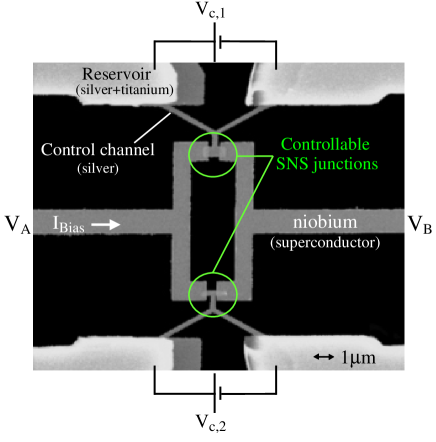
A practical realization of a controllable -SQUID is shown in Fig. 1. A niobium loop (thickness: 50 nm, surface area: 12 ) has two metallic weak links made of silver (thickness 50 nm). The length of the normal regions of both junctions is 1100 nm with a Nb separation of 420 nm. The width of the normal regions is 520 nm for the top junction and 220 nm for the bottom junction. The silver weak links are each connected to a V-shaped silver control channel with a total length of 5+1 which connects to two large silver reservoirs of 475 nm thick and a surface area of about . The size of the reservoirs is needed because they should act as effective cooling fins to prevent unwanted electron heating at T1K[18, 19]. The resistance per square of the normal region of the junction and the control channel is 0.4 , which yields, using free electron theory, an elastic mean free path of 46 nm with diffusion constant D=0.02 . The Thouless energy, estimated from the junction dimensions, is identical for both junctions and given by =12.
The geometry of the controllable Josephson junction used in the controllable SQUID differs from the conventional cross shape. The disadvantage is that the length L of the control channel is much larger than in the case of a cross shaped device, resulting in a diffusion time . As a consequence, a material with a long electron-electron relaxation time is needed to be able to maintain a non-thermal energy distribution in the control channel. For this reason silver is used as the normal metal[20, 21].
We now describe the sample fabrication, again referring to Fig. 1. The samples have been realized on a thermally oxidized Si wafer that is covered with a 150 nm layer of sputter deposited to improve the adhesion of Ag. In the first step the Nb ring is deposited using standard e-beam lithography on a double layer of PMMA, DC sputtering and subsequent lift-off. The critical temperature of the sputtered film is 8.1 K. Subsequently the silver normal region, control channel and the reservoirs are deposited in one single step using shadow evaporation. This is needed because the adhesion of Ag is so poor that it is not possible to bake this film to be able to do another lithography step. We use a double layer of PMMA-MA and PMMA with e-beam lithography and wet etching to create a PMMA suspended mask. The deposition is done in an UHV deposition system with a background pressure of mBar, the pressure in the system during the evaporation steps is mBar. Prior to deposition we use Argon etching ( mBar, 500 V) for 3.5 minutes to clean the Nb surface. After that we deposit 10 nm of Ti adhesion layer under a large angle (47o), with the result that the Ti layer is only deposited on the substrate at the position of the reservoirs, whereas it will be deposited on the sides of the resist at the position of the thin openings defining the control channel and the normal region of the junction. Subsequently we deposit 50 nm Ag perpendicular to the substrate, thus creating the control channel and the normal region of the junction. As a last step 700 nm of Ag is deposited again at 47o to form the reservoirs with an effective thickness of 475 nm. To measure the quality of the Nb-Ag interface we have made, in the same run, a cross of a 200 nm wide Nb and Ag wire. The resistance of the 200x200 nm interface has been determined to be 0.1 which is smaller than the square resistance of the Silver (0.4 ), indicating that the interface is clean. The SQUID shown in Fig.1 has a normal state resistance of 0.55 and, at 1.4 K, an equilibrium supercurrent (, mV) of 10 . The theoretical prediction of the is 0.5, [22], which corresponds well with the measured value of .
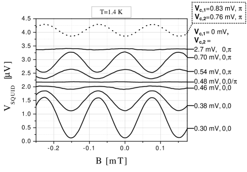
In the experiment, we bias the SQUID with a low frequency AC bias current (, 80Hz) with an amplitude a little larger than the critical current of the SQUID (see Fig 1) and measure the voltage over the SQUID, , as a function of the applied magnetic field B using a lock-in amplifier. This lock-in technique strongly reduces the noise compared to a DC biased measurement. Simultaneously we send a DC current through the top and/or bottom control channel and measure the resulting control voltage and/or . Measurements are performed at 100 mK, 1.4 K and at 4.2 K. A typical result, taken at 1.4 K using the device shown in Fig 1, is shown in Fig 2. The solid lines represent the -B oscillations for increasing values of () using . At first the amplitude of the oscillations decreases with increasing and reaches zero at =0.48 mV, indicating that the critical current of the bottom junction is equal to 0. At higher values of the -B oscillations re-appear, with a shift in phase with respect to the oscillations at lower values of . The bottom junction and hence the SQUID, are now in the state. At zero field we now measure a voltage maximum in stead of a minimum, indicating that a circulating current is now flowing around the SQUID loop. If the bottom junction is now kept in the -state (=0.76 mV), and is increased to 0.83 mV, the top junction switches to the -state as well. This corresponds to an addition of 2 times to the phase of the SQUID loop. In this case the original phase of the V-B oscillations is regained, as shown by the dashed line in the figure. Similar measurements at 100 mK in a dilution refrigerator have shown similar results, with however larger amplitudes of the V-B oscillations due to the temperature dependence of the critical current of the Josephson junctions.
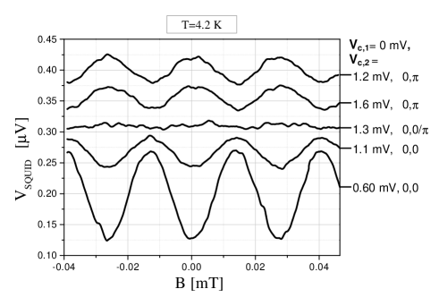
The question now arises whether the transition to a -state would be possible at 4.2 K. To be able to observe the effect at these higher temperatures we have made another set of samples, that differ only in the fact that the Josephson junctions are shorter (length of the normal region: 870 nm, width 500 nm, separation of the Nb electrodes: 260 nm, Rn=0.29 , =19 ) and that the surface area of the SQUID is 70.5 . We performed a measurement of the V-B oscillations as a function of (=0) at 4.2 K, with an AC current bias of 1.5 A. The results are shown in Fig. 3. It is clear from the figure that despite a reduction in the signal amplitude, due to the lower critical current and the lower normal state resistance, the transition to the state is observed at mV. This is a much higher value than in the previous experiment, caused by the elevated temperature and the larger Thouless energy. The observation of the -state at this temperature is somewhat surprising, for the transition to a -junction has so far only be observed at T100 mK.
In summary, we have shown that it is possible to fabricate a controllable - SQUID, based on Nb-Ag, which operates in the temperature range of 0.1 -4.2 K. The critical current of each junction can be controlled by means of the application of a control voltage over additional contacts attached to the normal region of the specific junction. Moreover, the role of the magnetic field, to apply and thereby to induce a circulating current in the SQUID, can be played by , which induces a screening current at integer external flux if its value is large enough to cause the junction enter a -state.
REFERENCES
- [1] J.Clarke in SQUID sensors, Fundamentals, Fabrication, and Applications, editted by H. Weinstock, NATO ASI Series 329, Dordrecht, 1-62 (1996).
- [2] M. Cryot and D. Pavuna, in Introduction to superconductivity and high-T materials , World Scientific, Singapore, (1992).
- [3] M. Tinkam, in Introduction to Superconductivity, McGraw-Hill, Singapore, (1996).
- [4] A.F. Morpurgo, T.M. Klapwijk and B.J. van Wees, Appl. Phys. Lett. 72, 966-968 (1998)
- [5] K. Neurohr, Th. Schäpers, J. Malindretos, S. Lachenmann, A.I. Braginski, H. Lüth, M. Behet, G. Borghs, A.A. Golubov, Phys. Rev. B 59, 11197 (1999).
- [6] J. Kutchinsky, R. Taboryski, C.B. Sorensen, J.B. Hansen and P.L. Lindelof, Phys. Rev. Let. 83, 4856 (1999)
- [7] A.F. Volkov, Phys. Rev. Lett. 74, 4730 (1995).
- [8] A.F. Volkov, H. Takayanagi, Phys. Rev. B. 56, 11184 (1997).
- [9] F.K. Wilhelm, G. Schön, A.D. Zaikin, Phys. Rev. Lett. 81, 1682 (1998).
- [10] S.-K Yip, Phys. Rev. B 58, 5803 (1998).
- [11] J.J.A. Baselmans, A.F. Morpurgo, B.J van Wees, T.M. Klapwijk, Nature 397, 43 (1999).
- [12] R.Shaikhaidarov, A.F.Volkov, H.Takayanagi, V.T.Petrashov. P.Delsing, Phys.Rev. B 62. R14649 (2000)
- [13] D.J. van Harlingen, Rev. of Mod. Phys. 67, 515 (1995)
- [14] V. V. Ryazanov, V. A. Oboznov, A. Yu. Rusanov, A. V. Veretennikov, A. A. Golubov, and J. Aarts Phys. Rev. Lett. 86, 2427 (2001)
- [15] E.J. Tarte, R.W. Moseley, M.R. Kölbl, W.E. Booij, G. Burnell and M.G. Blamire Supercond. Sci. Technol. 13, 983 (2000).
- [16] H. Pothier, S.Guéron, N.O. Birge, M.H. Devoret, Phys. Rev. Let. 79, 3490 (1997).
- [17] J.J.A. Baselmans, B.J. van Wees, T.M. Klapwijk, Phys. Rev. B 63, 094504 (2000)
- [18] F. C. Wellstood, C. Urbina, J. Clarke, Phys. Rev. B 49, 5942 (1994).
- [19] M. Henny, S. Oberholzer, C. Strunk , C. Schönenberger, Phys. Rev. B 59, 2871 (1999)
- [20] F. Pierre, H. Pothier, D. Estève, M.H. Devoret, J. of low Temp. Phys. 118, 437 (2000).
- [21] We have made a SNS junction identical to the ones used in the controllable SQUID using 50 nm of Cu as the normal region and control channel. Only a monotonic decrease of the supercurrent has been observed in this sample as a function of (T=1.4K).
- [22] P. Dubos, H. Courtois, B. Pannetier, F.K Wilhelm, A.D. Zaikin, and G. Schön, Phys. Rev. B, 63, 064502 (2001)