The Superconducting Gap in MgB2:
Electronic Raman Scattering Measurements of Single Crystals
Abstract
Polarisation-resolved Raman scattering measurements were performed on MgB2 single crystals to determine the magnitude, symmetry and temperature dependence of the superconducting gap. A single sharp peak due to Cooper pair breaking appears in the electronic continuum below , reaching an average maximum Raman shift of cm-1 () and showing up to 5 cm-1 anisotropy between polarised and depolarised spectra. The temperature dependence of follows that predicted from BCS theory, while the anisotropy decreases with decreasing temperature. It is concluded that the Raman results are consistent with a slightly anisotropic s-wave gap in a conventional BCS superconductor.
pacs:
PACS numbers: 74.25.Gz, 74.70.Ad, 78.30.ErThe recently discovered superconductor MgB2 [1] shows an unusually high for a simple binary compound, immediately raising questions regarding the nature of superconductivity in this material [2, 3, 4, 5, 6, 7]. Experiments on polycrystalline samples generally support a gap of s-like symmetry, but measurements of the gap magnitude vary widely. Some groups report a single superconducting gap, with gap-to- ratios ranging from 0.6 to 5 [8, 9, 10, 11], while other groups find multiple gap-like features with gap-to- ratios around 1.1–1.8 and 3.5–4.8 [12, 13, 14, 15]. Due to the difficulties and uncertainties associated with polycrystal measurements, these results strongly motivate further study of the gap feature(s) in single crystals.
Electronic Raman scattering is a useful experimental technique for studying superconductors because it provides a direct probe of the superconducting gap via the breaking of Cooper pairs by the incident light [16]. The frequency, polarisation dependence and temperature dependence of the pair breaking peak reflect the magnitude, symmetry and temperature dependence of the gap [16, 17, 18]. Knowledge of these fundamental properties is essential for the underlying mechanism of superconductivity to be deduced. For polycrystalline samples, the MgB2 Raman spectrum presents a broad phonon feature superimposed on a relatively intense electronic continuum [15, 19, 20], the latter undergoing a superconductivity-induced renormalization which has been interpreted in terms of two gaps of magnitudes () 44 cm-1 and 100 cm-1 [15]. In this letter we report the first Raman measurements of the fundamental gap properties in single crystals of MgB2.
Single crystals of MgB2 were synthesized from a precursor mixture of 99.9% pure magnesium powder and 97% pure amorphous boron. The crystals were grown in a BN container under 4–6 GPa pressure at 1400–1700∘C for 5 to 60 minutes. Magnetization and resistivity measurements give K with a transition width of 0.3 K [21]. Four circle XRD measurements indicate these are high quality single crystals, with no evidence of bulk impurities. Slab-like crystals with relatively clean and flat in-plane surfaces were selected for measurement. These crystals exhibited broken hexagonal shape of typical dimension 200–300 m square by 30–40 m thick. The crystals were mounted for in-plane measurement and oriented with the a-axis horizontal, within , confirmed by x-ray diffraction measurements. Further confirmation was provided by the results of superconducting-state Raman measurements. The incident light was polarised either vertically (V) or horizontally (H), that is, either perpendicular or parallel to the a-axis. Only vertically polarised scattered light was collected. In the point group, VV polarisation selects excitations of and symmetry, while HV polarisation selects only the component. Henceforth the VV and HV configurations will be referred to as polarised and depolarised.
Raman spectra were measured with a Jobin-Yvon T64000 triple monochromator, charge coupled device, and an excitation wavelength of 514.5 nm provided by an Ar-Kr laser. The typical incident power was 0.8 mW, point-focussed to a spot of 100 m diameter. To determine the degree of laser overheating, spectra were also measured at laser powers higher than typical. The only noticeable effect of higher incident powers was spot heating, and where appropriate subsequently quoted temperatures have been corrected for this effect. Temperature control was provided by a closed-cycle helium refrigerator and at typical laser powers sample overheating was estimated to be less than 2 K. All spectra have been corrected for the Bose thermal contribution.
Polarised and depolarised Raman spectra of a single crystal of MgB2 (crystal A) from 15 to 1300 cm-1 are shown in Fig. 1. The spectral intensity has been normalised at high wavenumbers and the polarised spectra
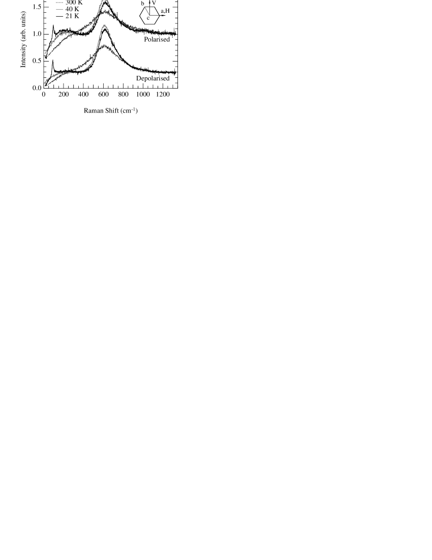
offset by 0.5 units along the y-axis. Dominating the spectra is a very broad, asymmetric feature located at around 620 cm-1, which is commonly attributed to the Raman-active E2g symmetry phonon in MgB2 [19, 20]. This feature narrows substantially with decreasing temperature, consistent with suggestions that the E2g phonon is very anharmonic [5], but curiously shows no indication of a large superconductivity-induced hardening below predicted by band theoretical calculations [4]. Cursory modelling of this feature with a Fano equation, an unsatisfactory description of the observed spectral lineshape, revealed 7–10 cm-1 hardening between 40 and 21 K. Further experiments must be performed to clarify the character of this mode.
In contrast, a clear superconductivity-induced renormalization of the electronic continuum is visible in the 21 K spectra, where a sharp pair breaking peak forms at around 100 cm-1. The magnitude of the renormalization is greater in depolarised spectra. Accompanying the peak is a decrease of scattering intensity at lower Raman shifts, although some scattering intensity remains directly below the peak. In the case of an isotropic s-wave gap the theoretically calculated electronic Raman spectrum is characterised by a pair breaking peak located at an energy of in all scattering channels, below which there is zero scattering intensity [16]. For anisotropic s-wave the scattering threshold remains, located at the minimum gap energy, while pair breaking peaks appear at different Raman shifts in different polarisations, reflecting the gap anisotropy [17, 18]. Since the polarisation dependence of the peak seen in MgB2 is not strongly anisotropic, we directly associate the pair breaking peak energy with .
Figure 2 shows Raman spectra from crystal A in the vicinity of the pair breaking peak. The spectra have been normalized to unity around 350 cm-1 and successive spectra have been progressively offset by one unit along

the y-axis. Where appropriate, temperatures have been corrected for sample heating effects. Here, the evolution of the peak with temperature is seen and a small anisotropy in peak energy between polarised and depolarised spectra is apparent. In the vicinity of 25 cm-1 the Raman intensity at low temperatures nearly vanishes. To obtain an estimate of the gap energy , the spectrum in the vicinity of the pair breaking feature was approximated by a Gaussian with a cubic background, and fitted with a least squares algorithm. Subsequently quoted uncertainties in are the 95% confidence intervals obtained from the fit. The average anisotropy between the two polarisations thus obtained is cm-1, the polarised peak always appearing higher in energy than the depolarised peak. Close examination of Fig. 2 suggests that the anisotropy is about 5 cm-1 at temperatures close to , and falls with decreasing temperature to a little less than 3 cm-1 at the lowest temperatures measured.
A number of single crystals were measured and low-frequency Raman spectra from a second crystal, crystal B, are shown in Fig. 3. In common with crystal A, a pair breaking peak appears in the superconducting state spectrum and agrees well between crystals. Anisotropy in is also present, amounting to cm-1 on average, about half that seen in crystal A. Some additional structure is also apparent. A sharp peak present in most crystal B spectra near 300 cm-1, but not present in crystal A, is attributable to surface contamination. Although the polarised spectra are comparable between crystals, additional scattering intensity is present in the depolarised spectra of crystal B. At low temperatures a

sharp shoulder forms around 30–40 cm-1, which is very similar to that seen in polycrystal results [15]. Residual scattering intensity in the vicinity of 25 cm-1 is non-vanishing in crystal B and the magnitude of the superconductivity-induced renormalization in the depolarised spectra is reduced compared to crystal A. Inspection of crystal B with an optical microscope showed a less regular surface and confirmed the presence of surface impurities. Typically, crystals with flat, clean surfaces showed a sharp peak with low residual scattering while crystals with evidence of surface disorder showed higher residual scattering and a shoulder at 30–40 cm-1.
Within the usual theoretical description of non-resonant electronic Raman scattering, the square of the Raman vertex weights scattering from different portions of the Fermi surface depending on the incident and scattered light polarisations [17]. Taking the band dispersion given by the nearest neighbour tight binding model [3] we made a straightforward calculation of for and symmetries and found that the former weights excitations from almost the entire hexagonal Brillouin zone, particularly near the vertices, while the latter weights excitations around the edges. Thus, the observation of a smaller gap magnitude in depolarised () spectra suggests an anisotropic in-plane gap of the form , compatible with s-wave symmetry [22].
In determining the superconducting gap symmetry, and thus placing constraints on the underlying mechanism of superconductivity, the temperature dependence of the gap provides another convenient test. BCS theory gives an explicit temperature dependence for a s-wave gap with which the experimental data may be compared.
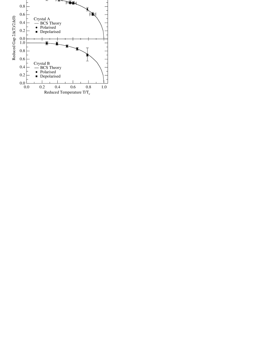
We calculate the reduced gap from our data, extrapolating from our lowest temperature measurements. Results of this calculation are shown in Table I.
| Sample | Polarisation | (cm-1) | |
|---|---|---|---|
| Crystal A | Polarised | ||
| Depolarised | |||
| Crystal B | Polarised | ||
| Depolarised |
The magnitude of the superconducting gap energy, averaged between polarisations, is , which is consistent with MgB2 being a moderately strong coupling superconductor. Figure 4 shows for both crystals, which follow the BCS-predicted temperature dependence. Uncertainties in temperature are shown for those data points to which correction was applied. The temperature dependence of the superconducting gap, as directly measured by Raman scattering, indicates that MgB2 is a conventional BCS superconductor.
The presence of Raman scattering intensity below 2 seen in Figs. 2 and 3 initially appears to contravene a simple s-wave interpretation of the data. The theory of Raman scattering in superconductors predicts a zero intensity threshold below the pair breaking peak in an s-wave superconductor [16, 17, 18] and Raman studies of the Nb3Sn and V3Si conventional superconductors [23, 24, 25] confirm a sharp decrease in scattering intensity below the 2 peak. In contrast, the high- superconductors exhibit broad, anisotropic pair breaking features which are accompanied by significant in-gap scattering intensity in all scattering channels, a consequence of the nodes in the d-wave gap function [17, 18]. Nodes in the gap function of MgB2 might explain the in-gap intensity seen below Tc in crystal A (Fig. 2), however this possibility is discounted by the near-isotropic polarisation dependence of the narrow pair breaking peak. While polycrystal measurements show gap-like features below 100 cm-1 [15], association of the 40 cm-1 shoulder with a second superconducting gap is problematic since it is not seen consistently in both crystals.
A number of extrinsic factors appear to contribute to the in-gap scattering present in Figs. 2 and 3. Rayleigh scattering, impurity and luminescence components, due to surface contamination, were present to varying degrees during the measurements, and the low-frequency tail of the very broad E2g phonon may also furnish scattering intensity at low frequencies. Significant surface disorder may introduce additional scattering contributions and the similar 40 cm-1 shoulder seen in polycrystal [15] and crystal B spectra may be related to a c-axis component of the superconducting gap. Such surface effects may also contribute scattering intensity to the below-gap Raman spectrum of crystal A, although to a much lesser degree. Clearly the 40 cm-1 shoulder is not an intrinsic feature of the in-plane Raman spectrum, related to a second pair breaking peak. Rather it appears to be an extrinsic effect related to sample surface quality.
In summary, we have measured the temperature and polarisation dependence of the pair breaking peak seen in the in-plane electronic Raman continuum of MgB2 single crystals. This peak shows BCS-like temperature dependence with only slight anisotropy, arguing strongly for conventional s-wave superconductivity. The average gap to ratio indicates moderately strong electron phonon coupling. We are able to identify only one gap feature in the in-plane Raman spectra, and attribute structure below the pair breaking peak seen in the poorer crystal to surface defects.
This work was supported by the New Energy and Industrial Technology Development Organization (NEDO) as collaborative research and development of fundamental technologies for superconductivity applications.
REFERENCES
- [1] J. Nagamatsu, N. Nakagawa, T. Muranaka, Y. Zenitani and J. Akimitsu, Nature410, 63 (2001).
- [2] J. M. An and W. E. Pickett, Phys. Rev. Lett.86, 4366 (2001).
- [3] J. Kortus, I. I. Mazin, K. D. Belashchenko, V. P. Antropov and L. L. Boyer, Phys. Rev. Lett.86, 4656 (2001).
- [4] Amy Y. Liu, I. I. Mazin, and J. Kortus Phys. Rev. Lett.87, 087005 (2001).
- [5] T. Yildirim, O. Gülseren, J. W. Lynn, C. M. Brown, T. J. Udovic, Q. Huang, N. Rogado, K. A. Regan, M. A. Hayward, J. S. Slusky, T. He, M. K. Haas, P. Khalifah, K. Inumaru and R. J. Cava, Phys. Rev. Lett.87, 037001 (2001).
- [6] M. Imada, J. Phys. Soc. Jpn. 70, 1218 (2001).
- [7] N. Furukawa, J. Phys. Soc. Jpn. 70, 1483 (2001).
- [8] T. Takahashi, T. Sato, S. Souma, T. Muranaka and J. Akimitsu, Phys. Rev. Lett.86, 4915 (2001).
- [9] G. Rubio-Bollinger, H. Suderow, and S. Vieira, Phys. Rev. Lett.86, 5582 (2001).
- [10] A. Sharoni, I. Felner and O. Millo, Phys. Rev. B63, 220508(R) (2001).
- [11] H. Kotegawa, K. Ishida, Y. Kitaoka, T. Muranaka and J. Akimitsu Phys. Rev. Lett.87, 127001 (2001)
- [12] P. Szabó, P. Samuely, J. Kačmarčík, Th. Klein, J. Marcus, D. Fruchart, S. Miraglia, C. Marcenat and A. G. M. Jansen, Phys. Rev. Lett.87, 137005 (2001).
- [13] F. Giubileo, D. Roditchev, W. Sacks, R. Lamy, D. X. Thanh, J. Klein, S. Miraglia, D. Fruchart, J. Marcus and Ph. Monod, Phys. Rev. Lett.87, 177008 (2001).
- [14] S. Tsuda, T. Yokoya, T. Kiss, Y. Takano, K. Togano, H. Kito, H. Ihara, and S. Shin, Phys. Rev. Lett.87, 177006 (2001).
- [15] X. K. Chen, M. J. Konstantinovic̀, J. C. Irwin, D. D. Lawrie and J. P. Franck, Phys. Rev. Lett.87, 157002 (2001).
- [16] M. V. Klein and S. B. Dierker, Phys. Rev. B29, 4976 (1984).
- [17] T. P. Devereaux and D. Einzel, Phys. Rev. B51, 16336 (1995); T. P. Devereaux and D. Einzel, Phys. Rev. B54, 15547 (E) (1996).
- [18] T. P. Devereaux, Phys. Rev. Lett.74, 4313 (1995).
- [19] A. F. Goncharov, V. V. Struzhkin, E. Gregoryanz, J. Hu, R. J. Hemley, H.-k. Mao, G. Lapertot, S. L. Bud’ko and P. C. Canfield, Phys. Rev. B64, 100509(R) (2001).
- [20] J. Hlinka, I. Gregora, J. Pokorný, A. Plecenik, P. Kúš, L. Satrapinsky and Š. Beňačka, Phys. Rev. B64, 140503(R) (2001).
- [21] S. Lee, H. Mori, T. Masui, Yu. Eltsev, A. Yamamoto and S. Tajima, J. Phys. Soc. Jpn. 70, 2255 (2001).
- [22] P. Seneor, C.-T. Chen, N.-C. Yeh, R. P. Vasquez, L. D. Bell, C. U. Jung, Min-Seok Park, Heon-Jung Kim, W. N. Kang and Sung-Ik Lee, Phys. Rev. B65, 012505 (2002)
- [23] S. B. Dierker, M. V. Klein, G. W. Webb and Z. Fisk, Phys. Rev. Lett.50, 853 (1983).
- [24] R. Hackl, R. Kaiser and S. Shicktanz, J. Phys. C 16, 1729 (1983).
- [25] R. W. Hackl, R. Kaiser and W. Gläser, Physica C 162–164, 431 (1989).