Titanium single electron transistor fabricated by electron-beam lithography
Abstract
A new method to fabricate non-superconducting mesoscopic tunnel junctions by oxidation of Ti is presented. The fabrication process uses conventional electron beam lithography and shadow deposition through an organic resist mask. Superconductivity in Ti is suppressed by performing the deposition under a suitable background pressure. We demonstrate the method by making a single electron transistor which operated at K and had a moderate charge noise of e/ at 10 Hz. Based on nonlinearities in the current-voltage characteristics at higher voltages, we deduce the oxide barrier height of approximately 110 mV.
pacs:
73.23.Hk, 73.40.Gk, 73.40.RwI Introduction
Single-charge devices have been studied intensively as possible alternatives for present day electronics (see, e.g., Ref. sets, ). Their operation is based on the fabrication of small enough tunnel junctions such that the energy of charging the tunnel junction capacitor, , where is the electron charge and the junction capacitance, is high compared to thermal fluctuations. Although direct applications of single electronics are still few, structures based on mesoscopic tunnel junctions have several fundamental uses in tunnel spectroscopy gueron ; mina , or as quantum limited detectors for the measurement of charge quantum bits schon ; korotkov1 . In most of these applications it is beneficial, if not necessary, to have the spectroscopic probe made from non-superconducting material, but simultaneously to maintain the essential parts of the circuit superconducting in order to observe quantum coherent behavior. Typically it is not possible to meet these criteria by oxidation of the aluminum leads that are part of the sample. In this work, we develop a reliable new method for fabrication of normal-insulator-normal tunnel barriers, which is based on the existing principles of e-beam lithography and shadow evaporation.
Electron-beam lithography with an organic polymer resist mask has served as the straightforward, flexible method to fabricate Al tunnel junctions offsetmask ; fultondolan . Since Al oxidizes easily and forms a several nm thick native oxide layer, yielding an almost vanishing tunnel conductance of mesoscopic junctions, sufficiently thin Al tunnel barriers (1-2 nm) are made in relatively low oxygen pressures of typically 0.1 mbar. Due to the high oxide barrier of Al2O3 of 1.5 V (Ref. al_oxide, ), current-voltage () curves do not become nonlinear due to barrier suppression effects at the low voltages relevant to the single-charge or spectroscopic experiments.
The fact that Al, having the property of easy oxidation, is a superconductor with bulk of about 1.2 K has certainly facilitated the way towards the nowadays good understanding of mesoscopic charging effects and superconductivity. Nevertheless, as already mentioned, there are several needs for tunnel barriers having normal counter electrodes also in zero external magnetic field. In fact, various techniques have been developed quite recently for this particular purpose. Guéron et al. gueron used thin, fully oxidized Al layers of nm on Cu. Some weakly oxidizing metals such as Ni and Gd have been oxidized by reactive evaporation react_ni or through oxygen glow discharge gadolin . Chromium forms a native oxide layer of 1-2 nm, with the desired property that the metal is not a superconductor. Normal-conducting SET transistors made of Cr have indeed been demonstrated kuzmin ; scherer , with controversial values for the barrier height of the Cr oxide: 170 mV (Ref. kuzmin, ), or 740 mV (Ref. scherer, ). However, controlled fabrication of Cr oxide junctions seems still difficult. Our attempts to oxidize Cr in various pressures of pure oxygen, or in air, consistently resulted in a short circuit in the junction.
II Fabrication techniques
Titanium seems a promising candidate material for fabrication of tunnel barriers. It forms a native oxide layer of nm, consisting mainly of TiO2 (Ref. vaquila, ), which could be a suitable barrier as such. Ti has been used to fabricate ultrasmall junctions by anodic STM nano-oxidation stm_tit1 ; rt_set ; stm_tit2 . These experiments give somewhat inconsistent values for the oxide barrier height between 178 mV (Ref. stm_tit2, ) and 285 mV (Ref. rt_set, ).
Although bulk Ti is superconducting with a of 0.39 K, the transition temperature decreases rapidly if the metal is dirty tit_tc . Vacuum evaporated films of Ti, even if deposited under UHV conditions, seem to be disordered enough that the falls well below temperatures accessible by small dilution refrigerators. Our Ti films evaporated at mbar exhibited a relatively large resistivity m and a RRR of 1.02. According to Ref. tit_tc, , a of 100 mK corresponds to a resistivity m. Since our films were considerably dirtier, we expect them to stay normal over the accessible temperature range down to 100 mK.
We used a standard double layer resist mask composed of 480 nm of copolymer and 120 nm of PMMA for the Ti shadow evaporation. Ti was e-beam deposited at room temperature at a rate of 1 nm/s at mbar. The deposited films seemed to have a tendency to spread some 50 nm around the main line. This behavior was markedly pronounced in films evaporated at higher pressures of mbar, where the metal had spread over the whole undercut area even several m wide. Since the spreading was strongly pressure dependent, we believe it was caused by scattering of Ti atoms in the vacuum region between the surface of the resist and the substrate. We first attempted to make tunnel junctions by e-beam depositing a second Ti layer after oxidation of the first layer. This always resulted in a short circuit, independent of the way the oxidation was performed. The problem was solved by making the counter electrodes by thermal evaporation of a Cu layer on top of the oxidized Ti. Apparently the oxide was broken during the second e-beam deposition, possibly by x-rays coming from the deposition target.
Along these lines, SET transistors were fabricated by first patterning the island by e-beam evaporation of 15 nm of Ti, followed by oxidation for 45 min in air. The electrodes were then made by thermal evaporation of 25 nm of Cu. We made a half dozen SET samples, all of which had reasonable room temperature resistances, scattered between 50 k and 15 M. One sample was cooled down to 100 mK. Initially it had a tunnel resistance k, but the resistance had increased during storage before cooldown up to M. This tendency of resistance increase with time seemed to be characteristic for all the fabricated junctions.
III Characterization of Ti SET
The measured SET device was rather asymmetrical (see inset of Fig. 1). The bigger junction had a geometrical area of about nm2, but in the smaller junction the films were hardly overlapping at all, and thus it was difficult to deduce its area accurately. The sample was cooled down to 100 mK in a plastic dilution fridge, the leads being filtered with 0.7 m of Thermocoax cable. The sample was characterized using voltage bias. -characteristics recorded at mK are shown in Fig. 1. Due to the high total tunnel resistance of the two junctions, M, current noise in the measurement system was a problem. The curves shown in Fig. 1 are a result of averaging over about 20 minutes. Gate modulation of the transistor was visible below 0.4 K. Immediately after cooldown there were strong fluctuations of the background charge, and the -curves didn’t stay stable. After several days, however, the background charge fluctuations settled down and the gate operation point did not change noticeably over tens of hours.
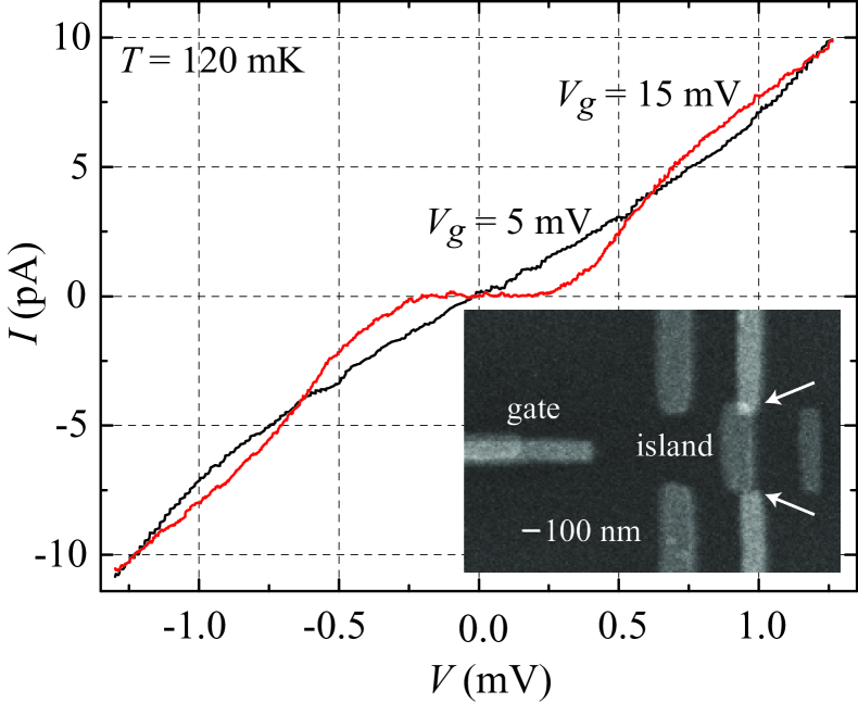
From the maximum width of the Coulomb blockade current plateau around zero voltage, mV, we derive the total island capacitance fF, and a charging energy of 1.8 K.
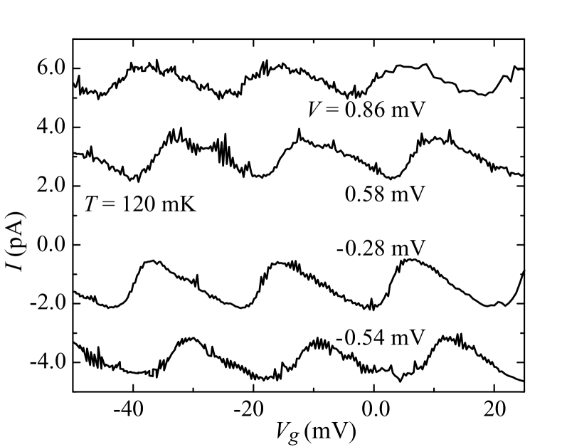
Gate modulation curves of the transistor at mK are shown in Fig. 2. Due to asymmetry of the device, the curves have different slopes at different sides of the maxima. Just beyond the Coulomb blockade threshold, absolute values of the positive and negative slope of the current modulation, at a fixed bias voltage, are given by
| (1) |
where is the gate period. In an asymmetrical device, the slopes are different because . On the basis of Eq. 1, we derive M, M, and . We thus would expect a total tunnel resistance of M, which is of the same order as the value M estimated directly from the -characteristics at low voltages rt_approx .
Assuming the capacitance is dominated by the contribution from the larger junction having the area nm, and using the oxide thickness Å determined in section IV, and the plate capacitor formula , we get a dielectric constant . This value is drastically smaller than the dielectric constants reported in literature for thin films of TiO2, (Refs. perm1, ; perm2, ; perm3, ). In fact, such a high permittivity would make the capacitance so large that single-charge effects would not be observable under our experimental conditions. Reduced dielectric constants have been reported in tunnel barriers made from other materials as well al_oxide ; scherer .
As discussed in section II, we do not expect our Ti films to go superconducting in the accessible temperature range. In a SET having a superconducting island but normal electrodes, the Coulomb blockade plateau is widened at both sides by the amount due to the energy gap of the superconductor. Thus, when an external magnetic field is applied to suppress superconductivity, onset of current should switch approximately by the voltage . We made this test by recording the current at a fixed voltage 0.32 mV just beyond the onset of the current branch in a zero field, and in a high enough applied field mT. Results of these two measurement series averaged to the same with standard errors of mean fA. We assume the effect of superconductivity immediately beyond the onset of current can be approximated simply by shifting the -curve along the voltage axis. then corresponds to a shift in voltage by V, which determines the minimum detectable gap V. Thus we have a minimum detectable critical temperature mK. When is compared to the measurement temperature of 100 mK, we conclude that the Ti films were not superconducting at 100 mK, in agreement with Ref. tit_tc, .
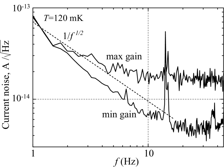
Current noise in the output of the Ti SET was measured in the voltage-biased configuration at different gate operation points of the transistor, and at different bias voltages. The noise spectra shown in Fig. 3 were measured at the bias mV (lowest curve in Fig. 2), in the region of maximum current modulation. Clearly, the noise at the maximum gain is larger than at the minimum gain. Below 10 Hz, the noise power follows roughly a behavior expected from a collection of two-level fluctuators. At higher bias points, the noise saturates at values comparable to those of maximum gain at low bias. At 10 Hz at the maximum gain of pA/e, we have a current noise fA/, which is translated to equivalent input charge noise e/. This figure is similar or slightly higher than what we have observed in ordinary Al SETs or what has been reported mooij_jap ; noise_gain , but considerably higher than the lowest figures so far, e/, observed in a stacked design stacknoise .
IV High voltage behavior
At voltages comparable to the height of the potential barrier in the insulating oxide, -curves become nonlinear as a consequence of suppression of the barrier. This opens up the possibility to characterize the barrier in terms of its height and width . Several authors kuzmin ; scherer have used a formula derived by Simmons simmons1 for the tunnel current density as
| (2) |
where , , and is a correction factor discussed below in more detail. The expression holds for a barrier of arbitrary shape and voltage provided is the mean barrier height above the Fermi level of the negatively biased electrode, and is the width of the barrier at the same position. For a symmetrical, rectangular barrier at low voltages , , and is constant and equal to the actual barrier width, .
Large scale -characteristics of our Ti SET are shown in Fig. 4. The asymmetry which is dependent on current direction can be explained by a tunnel barrier which is asymmetrical due to different work functions of the electrodes. In fact, our situation is rather complicated due to the presence of two asymmetrical tunnel junctions having different resistances. However, because the ratio of junction resistances was of the order 4, we made the simplifying assumption of ignoring the smaller resistance junction in fitting the Simmons’ theory to our data.
As shown in the discussion of asymmetrical tunnel barriers in Ref. solids, , the differential conductance of a barrier between electrodes having different work functions and is symmetric about the voltage . Indeed, our data has this symmetry property with respect to a +15 mV shift in conductance if the Coulomb blockade contribution is excluded (data not shown). At larger voltages, there is a similar symmetry about -45 mV. These shifts can be traced back to the larger and smaller resistance junctions, respectively. Ratio of the shifts agrees reasonably well with the estimated junction resistance ratio. These data thus indicate a work function difference of 10-15 mV for the Cu-Ti pair in this configuration work_f .
Although the correction factor has been ignored in earlier studies on symmetric junctions kuzmin ; scherer , it should not be neglected since otherwise an error of tens of % in the fitted parameters is expected. This cast some doubts on the parameters obtained for Cr junctions in Refs. kuzmin, ; scherer, . In our case it is necessary to include , since it is the only factor that gives rise to asymmetry in the -characteristics hartman .
Let us now consider the asymmetrical, trapezoidal barrier with heights and (Refs. hartman, ; simmons2, ), shown in the inset of Fig. 4 (a). If electrode 1 is negatively biased, the net electrical current density flows to direction 1 and is denoted by . In the case of opposite polarity, the net current density flows to direction 2 and is denoted by . For the asymmetrical barrier, generally . In the following, the subscripts 1 and 2 refer to and , respectively.
IV.1 Simmons’ theory, intermediate voltages:
The average barrier heights at voltages satisfying (without loss of generality, we take to be the lower barrier) are equal and are given by . The net current density is given by Eq. 2, with
| (3) |
The net current density is given by Eq. 2 as well, with
| (4) |
Equation 2, when substituted with Eqs. 3 and 4, should describe the -characteristics at intermediate voltages . Because the area of the large resistance junction was not known accurately, we scaled the current density with a free fitting parameter. Before fitting, the voltages were multiplied by the factor to account for division of the applied voltage across the two junctions, using their zero-voltage resistance ratio . However, the fit turned out to be poor especially at low voltages, in accord with experiments on Cr junctions kuzmin ; scherer . In contrast to the experimental data, theory predicts that at low voltages and are almost equal. The discrepancy could not likely be explained by effect of the second junction either. Fit of the whole experimental data to and determined the parameters mV, mV, and Å. However, the reliability of these fits is weakened by the fact that several other parameter combinations resulted in seemingly similar curves. Barrier heights in this range are, however, favored by other arguments as discussed in the next paragraphs.
IV.2 Simmons’ theory, high voltages:
The intersection voltage of the two current branches and , marked as in the data in Fig. 4, offers another, probably better, way to determine the barrier height. The intersection occurs in the high voltage regime, . The currents are still given by Eq. 2, but now with , for , and and for . For both and , .
Numerical calculations of the intersection voltage indicate if and differ by at most 10-20 %. From Fig. 4 we have mV. Thus, after correcting for voltage division due to the second junction, we have mV. is calculated with the independently determined value mV, to determine mV. These parameter values are in reasonable agreement with the fits to the Simmons’ theory in the intermediate-voltage regime, but not with results of former work: 178 mV (Ref. stm_tit2, ), 285 mV (Ref. rt_set, ).
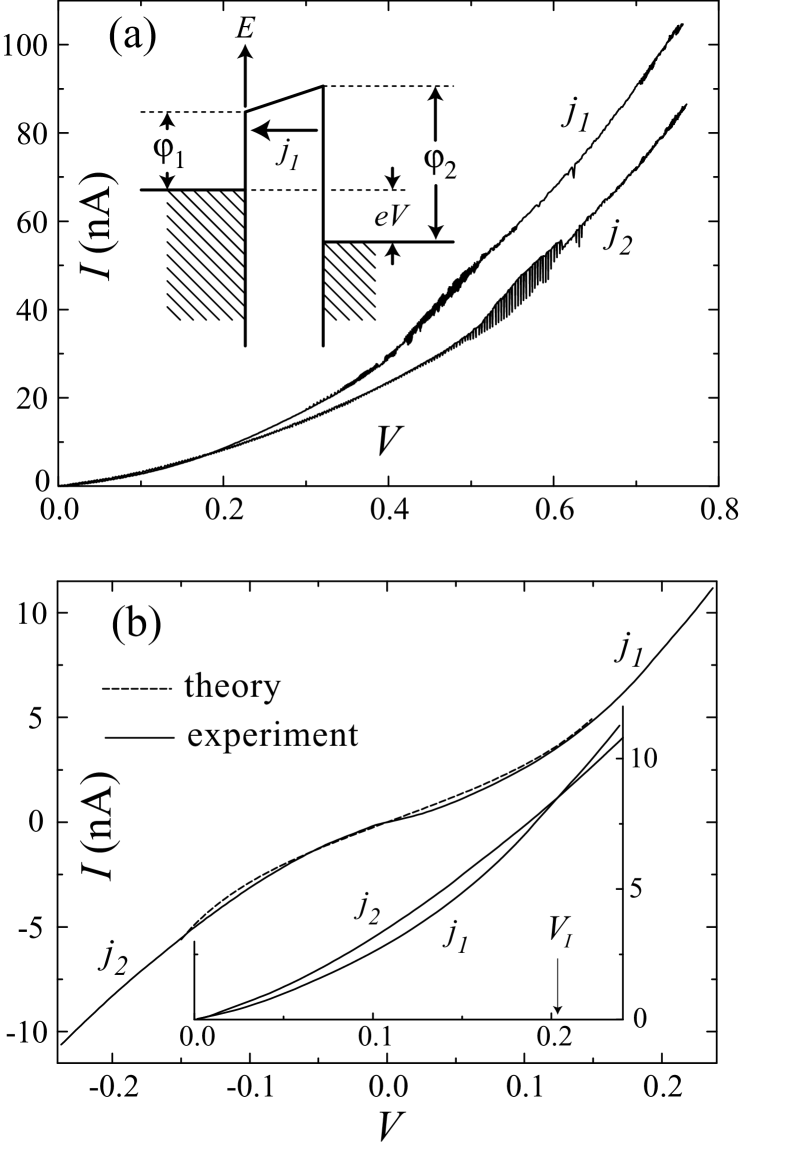
Around voltages of approximately +0.4 V and -0.5 V, there is a noisy section in the -curves, followed by a change in resistance. Similar effects were observed in Cr oxide junctions by Scherer scherer , and interpreted as being caused by charge traps in the barriers activating by a suitably high electric field, thus giving rise to additional current paths. The enhanced conductance in our case just beyond the noisy section agrees well with this explanation.
V Summary and conclusions
We have developed a straightforward and reliable way to fabricate normal tunnel barriers by oxidation of titanium in air. The method can find several uses in fundamental research or in applications. We use the method to fabricate a single electron transistor which performs comparably to traditional Al SETs. Nonlinearities in the -characteristics at higher voltages indicate the height of the TiO2 barrier of 110 mV, and width of 16 Å.
Acknowledgements.
The authors would like to thank Hansjörg Scherer for useful information. This research was supported in part by Emil Aaltonen foundation, and by the Human Capital and Mobility Program ULTI of the European Union.References
- (1) D. V. Averin and K. K. Likharev, in Mesoscopic Phenomena in Solids, edited by B. L. Altshuler, P. A. Lee, and R. A. Webb (Elsevier, Amsterdam, 1991).
- (2) S. Guéron, H. Pothier, N. O. Birge, D. Esteve, and M. H. Devoret, Phys. Rev. Lett. 77, 3025 (1996).
- (3) M. A. Sillanpää, T. T. Heikkilä, R. K. Lindell, and P. J. Hakonen, e-print cond-mat/0102367.
- (4) A. Shnirman and G. Schön, Phys. Rev. B 57, 15400 (1998).
- (5) A. N. Korotkov, Phys. Rev. B 63, 115403 (2001).
- (6) G. J. Dolan, Appl. Phys. Lett. 31, 337 (1977).
- (7) T. A. Fulton and G. J. Dolan, Phys. Rev. Lett. 59, 109 (1987).
- (8) M. Maezawa, M. Aoyagi, H. Nakagawa, I. Kurosawa, and S. Takada, Appl. Phys. Lett. 66, 2134 (1995).
- (9) C. H. Shang, G. P. Berera, and J. S. Moodera, Appl. Phys. Lett. 72, 605 (1998).
- (10) P. LeClair, J. S. Moodera, and R. Meservey, J. Appl. Phys. 76, 6546 (1994).
- (11) L. S. Kuzmin, Yu. A. Pashkin, A. N. Tavkhelidze, F.-J. Ahlers, T. Weimann, D. Quenter, and J. Niemeyer, Appl. Phys. Lett. 68, 2902 (1996).
- (12) H. Scherer, Th. Weimann, P. Hinze, B. W. Samwer, A. B. Zorin, J. Niemeyer, J. Appl. Phys. 86, 6956 (1999).
- (13) I. Vaquila, M. Passeggi, and J. Ferrón, J. Phys.: Condens. Matter 5, 157 (1993); I. Vaquila, M. Passeggi, and J. Ferrón, Phys. Rev. B 55, 13925 (1997).
- (14) K. Matsumoto, S. Takahashi, M. Ishii, M. Hoshi, A. Kurokawa, S. Ichimura, and A. Ando, Jpn. J. Appl. Phys. 34, 2B, 1387 (1995).
- (15) K. Matsumoto, M. Ishii, K. Segawa, Y. Oka, B. J. Vartanian, and J. S. Harris, Appl. Phys. Lett. 68, 34 (1996).
- (16) B. Irmer, M. Kehrle, H. Lorenz, and J. P. Kotthaus, Appl. Phys. Lett. 71, 1733 (1997).
- (17) J. Vangrunderbeek, C. van Haesendonck, and Y. Bruynseraede, Phys. Rev. B 40, 7594 (1989).
- (18) It is rather difficult to deduce from the -curve. At low voltages the curve has nonlinearities due to Coulomb effects, and at higher voltages, due to barrier suppression.
- (19) T. Fuyuki and H. Matsunami, Jpn. J. Appl. Phys. 25, 1288 (1986).
- (20) W. D. Brown and W. W. Grannemann, Solid State Electron. 21, 837 (1978).
- (21) S. A. Campbell, H. S. Kim, D. C. Gilmer, B. He, T. Ma, and W. L. Gladfelter, IBM J. Res. Develop. 43, 383 (1999).
- (22) S. M. Verbrugh, M. L. Benhamadi, E. H. Visscher, and J. E. Mooij, J. Appl. Phys. 78, 2830 (1995).
- (23) B. Starmark, T. Henning, T. Claeson, P. Delsing, and A. N. Korotkov, J. Appl. Phys. 86, 2132 (1999).
- (24) V. A. Kruperin, D. E. Presnov, A. B. Zorin, and J. Niemeyer, J. Low Temp. Phys. 118, 287 (2000).
- (25) J. G. Simmons, J. Appl. Phys. 34, 1793 (1963).
- (26) J. M. Rowell, in Tunneling phenomena in solids, edited by E. Burstein and S. Lundqvist (Plenum, New York, 1969).
- (27) is sensitive to the particular configuration, such as crystal direction. Tabulated values, N. W. Ashcroft and N. D. Mermin, Solid State Physics (W. B. Saunders, Philadelphia, 1976); CRC Handbook of Chemistry and Physics, 78th edition, (CRC Press, New York, 1997), would indicate mV.
- (28) T. E. Hartman, J. Appl. Phys. 35, 3283 (1964).
- (29) J. G. Simmons, J. Appl. Phys. 34, 2581 (1963).