Giant microwave photoresistance of two-dimensional electron gas
Abstract
We measure microwave frequency (4-40 GHz) photoresistance at low magnetic field , in high mobility 2D electron gas samples, excited by signals applied to a transmission line fabricated on the sample surface. Oscillatory photoresistance vs is observed. For excitation at the cyclotron resonance frequency, we find an unprecedented, giant relative photoresistance of up to 250 percent. The photoresistance is apparently proportional to the square root of applied power, and disappears as the temperature is increased.
pacs:
73.50.Pz, 73.50.-hThe two dimensional electron gas (2DEG) in GaAs/AlxGa1-xAs heterojunctions has long been known to exhibit resonant photoresponse to illumination at the cyclotron resonance frequency, . This resonant response has generally been attributed to heating of the electrons by absorption of energy from the radiation field. The earliest photoresistance experiments on 2DEG, in both the far infrared (FIR)maantsui ; horstman and millimeter wavevasilnodots regimes, showed single, well-defined positive photoresistance features near the cyclotron resonance condition, , where is the applied frequency and is the effective mass in GaAs, and is the cyclotron frequency, . , the change of dc resistance due to applying radiation, divided by the resistance with the radiation off, was much less than unity.
Later workzudov for to 150 GHz, used higher mobility samples (, about three times that in the earlier investigationvasilnodots ), and revealed of large relative size, with larger . Strikingly, vs showed oscillations with alternating positive and negative . These oscillations were periodic in like Shubnikov-de Haas (SdH) oscillations, but had -dependent period . peaks occurred at , for . The peak was largest but peaks for up to 7 were observed. To explain the oscillatory photoresistance the authors of ref. zudov , proposed a process in which impurity scattering combines with microwave absorption at . This causes transitions between Landau orbitals with energy quantum numbers differing by and guiding centers displaced from each other.
In this paper we report on photoresistance measurements, in which microwaves were applied to a transmission line made of metal film on the top surface of the sample. We find an oscillatory whose maximum value is 2.5, nearly an order of magnitude larger than previously observedzudov . The giant photoresistance decreases with , and is proportional to the incident microwave amplitude, that is, to the square root of the applied power.
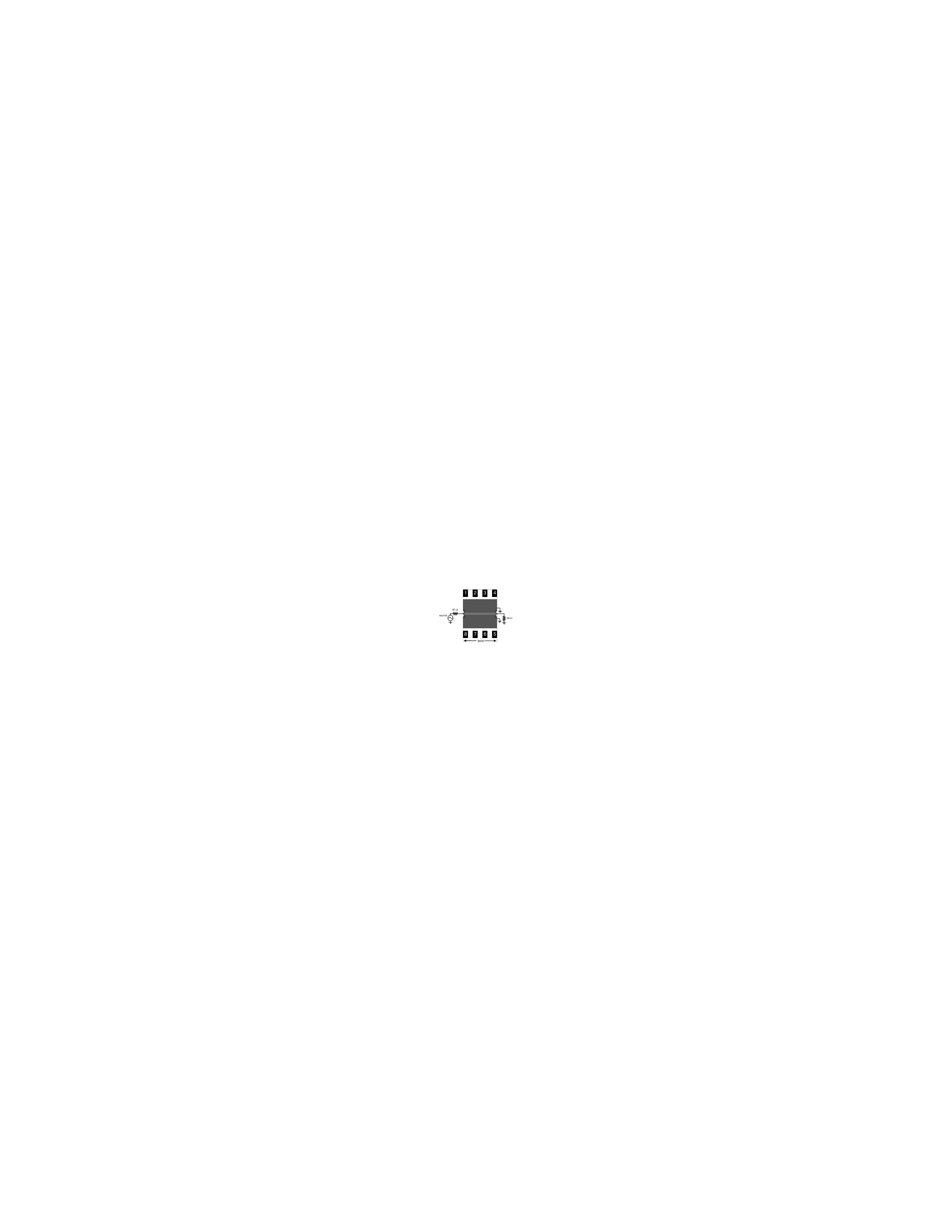
We performed measurements on samples originally designed for broadband, transmission line based measurements of the microwave conductivity of the 2DEGengel . Fig. 1 is a schematic illustration of a sample. On the top surface of the 3 5 mm sample, a film of 200 Å Ti and 3500 Å Au was patterned to form a coplanar waveguide (CPW)wen transmission line, with a 30 m wide center strip separated from side ground planes by slots of 20 m-width, which are shown in light grey in the figure. In the limit of low 2DEG conductivity, the in-plane microwave fields produced by driving the CPW are well-confined within the slots; in the present experiments some of the microwave field leaks under the metal film near the slot. We studied the change, on applying microwaves to the CPW, of quasi-dc resistance measured using combinations of the alloyed AuGe/Ni contacts at the edges, marked 1 through 8 in the figure. The 2DEG under the tapers of the CPW at the edges of the sample (the areas indicated by the dashed lines in Fig. 1) was removed by chemical wet etching. The rest of the sample was not etched, so the ohmic contacts are connected to the slot areas by the 2DEG under the ground planes.
We measured two samples, both made from the same wafer, a high-mobility GaAs-AlGaAs heterojunction in which the 2DEG was located approximately 120 nm underneath the sample surface. Sample 2, but not sample 1, contained an antidot array, which was placed just in the two CPW slots. To produce the antidots, 500 nm period square lattices of 50 nm diameter, 50 nm deep holes were defined by electron beam lithography and reactive ion beam etchingvawter . The samples were prepared for measurement with a brief illumination from a red LED, after which 0.3 K mobility (without antidots) was around 3 to . As determined from Shubnikov-de Haas (SdH) oscillations in vs , the densities of sample 1 and sample 2 were respectively 1.7 and 2.1 cm -2.
The quasi-dc resistance measurements used typical operating frequency of 13.5 Hz, and applied current of 100 nA rms. We report resistances, , measured from four contacts along one edge of the sample, in the topology associated with diagonal resistivity, with injected current between contacts 1 and 4 on Fig. 1 , and voltage taken between contacts 2 and 3. With the microwaves both off and on, some asymmetry of between positive and negative was present in sample 1 , and to a much lesser extent in sample 2. We attribute this asymmetry to inhomogeneity produced by illumination, and to the large size and close proximity to each other of the contacts. All the presented here are the average of data taken at and .
The samples were measured in a dilution refrigerator cryostat. A Hewlett Packard 8722D network analyzer at room-temperature supplied microwave signals to cryogenically compatible coaxial cables that were connected to the CPW. The external magnetic field () was normal to the plane of the 2DEG.
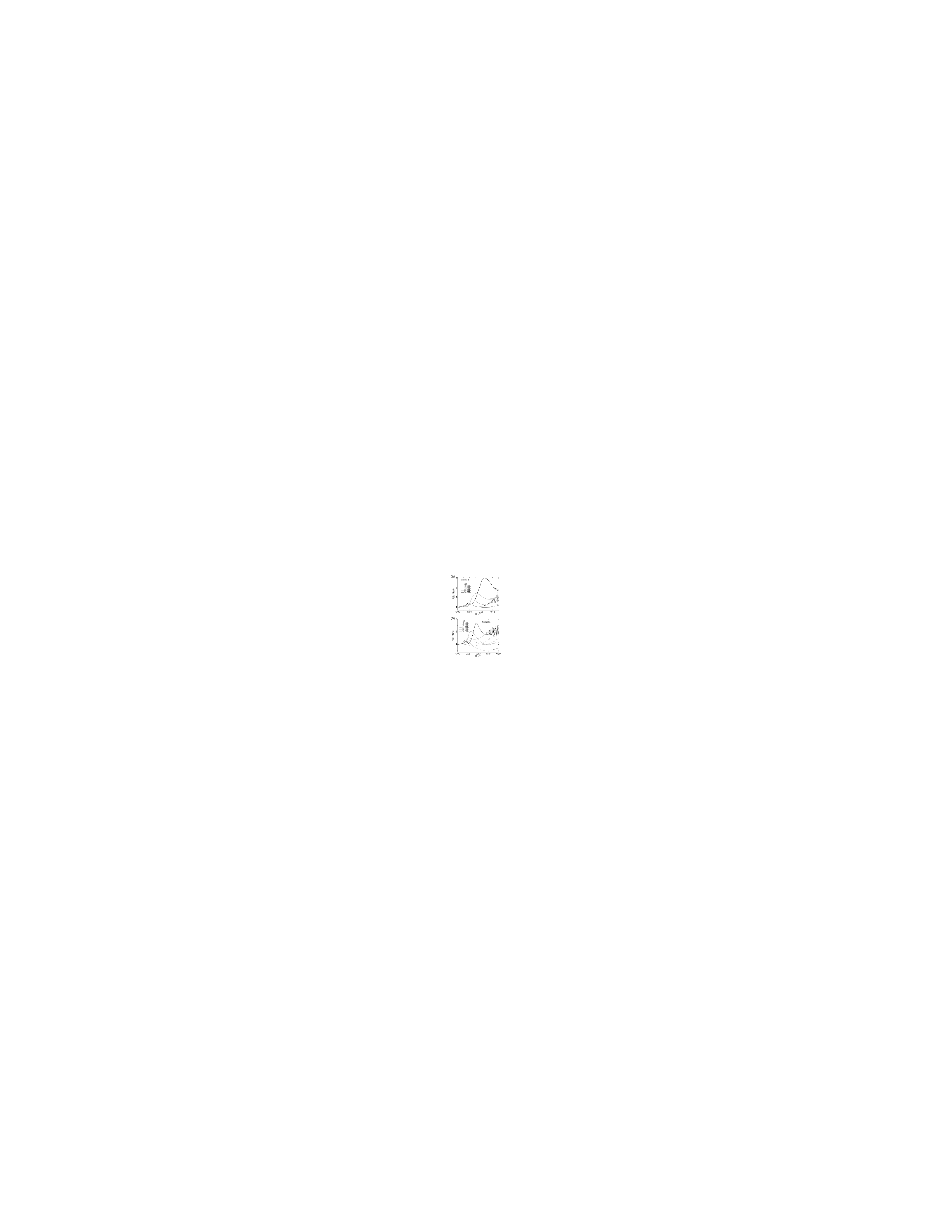
Fig. 2a shows vs for sample 1. Along with a reference trace taken with the microwave source off, traces are shown for several applied microwave frequencies, . The microwave power was 100 nW at 50 ohms, incident onto the edge of the CPW. The “bath” temperature (that of the metal on which the sample was mounted) was about 100 mK, but heating due to the applied power must have occurred. When microwaves are incident on the CPW, vs exhibits a series of peaks. As increases, the oscillations shift to higher and grow stronger, and more features emerge at lower . For GHz there are three peaks, which we will see have roughly even spacing in .
Data for sample 2 (with antidots in the CPW slots) are shown in Fig. 2b. The oscillations exist similar to sample 1. The different behavior of the two samples, both with and without the microwaves, are likely due to different red-light illumination doses rather than to the presence of the antidots in sample 2. The antidots have little effect on the measurement since the measuring contacts are all on one side of the antidot strips and so are somewhat remote from them.
Our main result is the large size of the photoresistance seen particularly on the highest- peak. There we find , the change in on applying microwaves divided by the microwaves-off value, as high as 2.5 for sample 1 and 2.0 for sample 2. The large cannot be explained by being made small by cancellation of Hall and diagonal contributions to the measured resistance, so it is clear that the application of the microwaves near resonance produces a drastic change in the transport of the 2DEG.
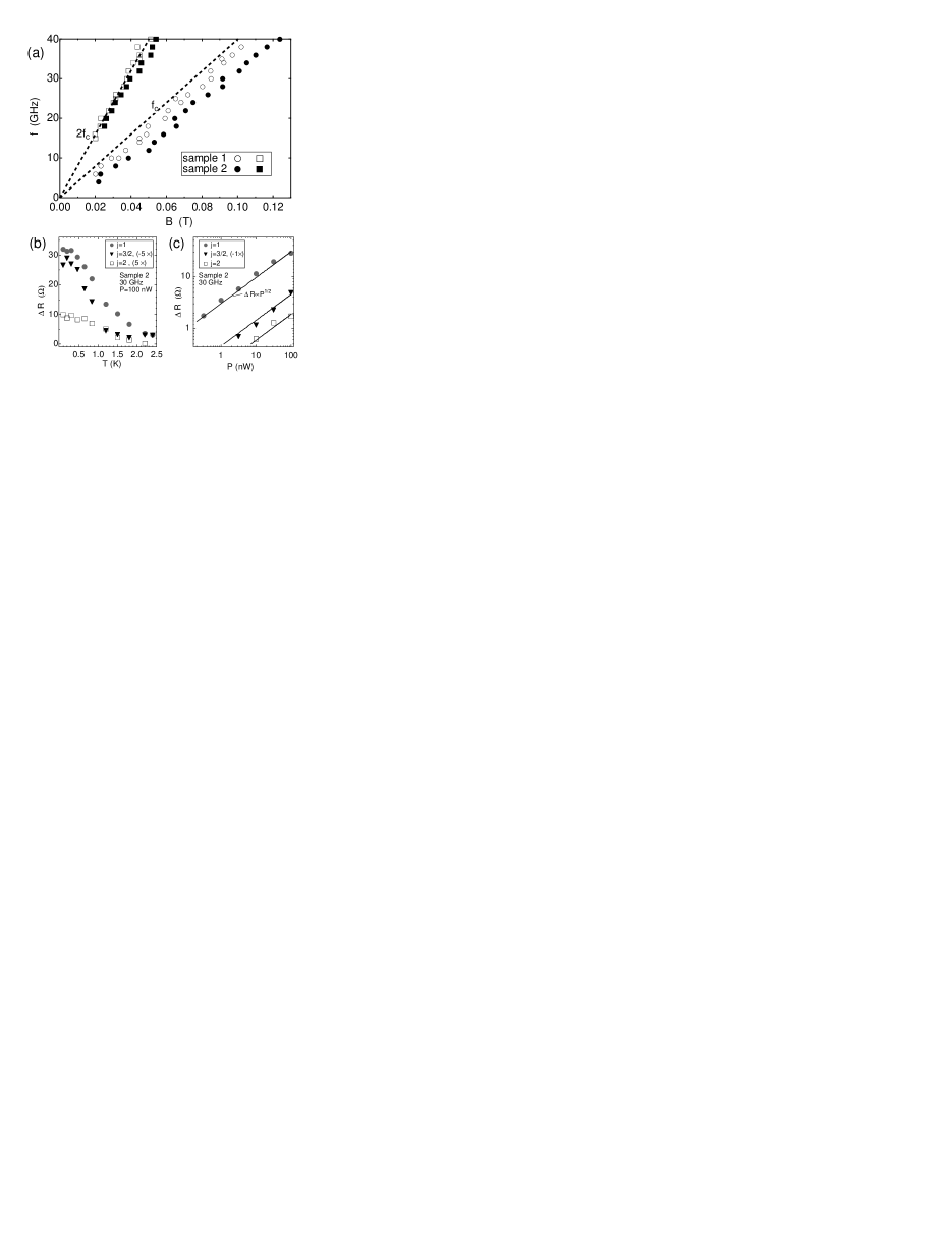
The photoresistance oscillations are related to as described in ref. zudov ; with , maxima occur at integer , and minima at half-integer . Fig. 3a shows the positions of the and microwave-produced maxima of both samples. The applied frequency, , is plotted against the at which the maximum occurs. and are also plotted, where we have used of 0.07 times the free electron mass. The maxima falling close to the lines demonstrates the approximate peridicity of the photoresistance oscillations. The highest () maximum falls at significantly higher than the line, especially for sample 2. The maximum falls on to within about 5 percent for both samples. Outward shift of the first harmonic was also reported in ref. zudov .
In Fig 3b, we plot vs for the 1,3/2, and 2 photoresistance extrema of sample 2, for nW, at GHz. is negative for , and positive for and 2. increases with decreasing , saturating around 500 mK. 30 GHz photons have energy at 1.43 K; vs is significantly reduced from its maximum by that temperature, and is likely characterized by that energy.
Fig. 3c shows vs , the microwave power incident onto the CPW, for sample 2 with GHz, at the and maxima and the minimum. The “bath” temperature, , to which the electrons cool in the limit of very small applied, was around 100 mK. Lines with appear on the graph; this behavior fits the data well and is at least consistent with the data for and . The behavior appears to hold well down to small , where heating of the sample would be much less. vs may be affected by (1) heating of the sample and by (2) reflectance of the CPW varying with . The second effect could make the microwave intensity that reaches the relevant area of 2DEG nonlinear in the power incident onto the CPW.
The samples we looked at have similar mobility to those examined in ref. zudov . The high ends of our and ranges overlap the conditions studied in that reference, for example at GHz, K. The much larger presently observed may be due to a larger power density reaching the 2DEG, or to inhomogeneity caused by the opaque ground planes upon illuminating the sample with red light.
In conclusion, we have found a low microwave photoresistance much larger than previously observed; the features have apparent dependence, and a characteristic .
We would like to thank W. E. Baca, J. Wang and J. Yao for technical assistance and C. M. Hu for valuable discussions. We especially thank R. R. Du for making ref. zudov available before publication. This work is supported by the Air Force Office of Scientific Research, and the National Science Foundation.
References
- (1) J. C. Maan, Th. Englert, and D. C. Tsui, Appl. Phys. Let. 40, 609 (1982).
- (2) R. E. Horstman, E. J. v.d. Broek, J Wolter, R. W van der Heijden, G.L. J. A. Rikken, H. Sigg, P. M. Frijlink, J. Maluenda and J. Hallais, Solid State Comm. 50, 753 (1984).
- (3) E. Vasiliadou, G. Müller, D. Heitmann, D. Weiss, K von Klitzing, H. Nickel, W. Schlapp, and R Lösch, Phys. Rev. B23, 17145 (1993).
- (4) M.A. Zudov, R.R. Du, J.A. Simmons and J.L. Reno, cond-mat/9711149; see also M.A. Zudov, R.R. Du, J.A. Simmons and J.L. Reno, submited for publication.
- (5) L.W. Engel, D. Shahar, Ç. Kurdak, and D.C. Tsui, Phys. Rev. Lett. 71, 2638 (1993); also in Physical Phenomena in High Magnetic Fields II, proceedings, (World Scientific, Singapore, 1996) 23.
- (6) C. P. Wen, IEEE Trans. Microwave Theory Tech., MTT-17, 1087 (1969).
- (7) G.A. Vawter, in Handbook of Advanced Plasma Processing Techniques, edited by R. Shul and S. Pearton (Springer, Berlin, 2000), 50.