Equilibrium Properties of Double-Screened-Dipole-Barrier SINIS Josephson Junctions
Abstract
We report on a self-consistent microscopic study of the DC Josephson effect in junctions where screened dipole layers at the interfaces generate a double-barrier multilayered structure. Our approach starts from a microscopic Hamiltonian defined on a simple cubic lattice, with an attractive Hubbard term accounting for the short coherence length superconducting order in the semi-infinite leads, and a spatially extended charge distribution (screened dipole layer) induced by the difference in Fermi energies of the superconductor and the clean normal metal interlayer . By employing the temperature Green function technique, in a continued fraction representation, the influence of such spatially inhomogeneous barriers on the proximity effect, current-phase relation, critical supercurrent and normal state junction resistance, is investigated for different normal interlayer thicknesses and barrier heights. These results are of relevance for high- grain boundary junctions, and also reveal one of the mechanisms that can lead to low critical currents of apparently ballistic junctions while increasing its normal state resistance in a much weaker fashion. When the region is a doped semiconductor, we find a substantial change in the dipole layer (generated by a small Fermi level mismatch) upon crossing the superconducting critical temperature, which is a new signature of proximity effect and might be related to recent Raman studies in Nb/InAs bilayers.
pacs:
PACS numbers: 71.27.+a, 74.50.+r, 74.80.Fp, 73.40.JnI Introduction
The Josephson effect [1] is one of the most spectacular phenomena arising from the macroscopic phase coherence of Cooper pairs. A dissipationless current flows at zero voltage between two superconductors weakly coupled through a tunnel barrier (, where and denote a superconductor and an insulating barrier, respectively) or weak links (, , etc., where stands for a constriction, and for a normal metal). The study of such inhomogeneous superconducting structures has been driven by both interest in the fundamentals of quantum mechanics, and by the potential application of Josephson junctions as circuit elements in electronic devices. [2]
Recently, considerable attention has been directed toward the study of junctions, [3, 4, 5] where the insulating tunnel barrier is split into two pieces separated by a normal metal. These types of junctions have provided a playground to study the interplay [6] between the mesoscopic coherence of a single-particle wave function in the normal metal and the macroscopic coherence of a many-body wave function of Cooper pairs. [7] Furthermore, the reexamination of various multilayered structures of the type in applied research has been driven by the struggle to optimize the performance of Josephson junctions in low-temperature superconducting (LTS) digital electronics.[8, 9, 10] In mesoscopic superconductivity, one frequently deals with -- junctions [3] ( being a heavily doped semiconductor with a two-dimensional electron gas) where the role of the layer is played by a space-charge layer arising at the - interface (additional scattering at the interface can occur from the mismatch between the effective electron masses and Fermi momenta in the and ). The technological advances in fabricating such hybrid structures [3] have given an impetus to the field of mesoscopic superconductivity [6, 7] where the two-dimensional electron gas is amenable to an engineering of its “metallic” properties; i.e, one can tune the Fermi wavelength, or mean free path, and one can confine electrons with gate electrodes. In such structures, phase-coherence of the electron and Andreev-reflected hole [11] at the interface can be studied without too much normal reflection, because the charge-accumulation layer arising at a typical Nb/InAs interface, or the Schottky barrier at a Nb/Si interface, are much more transparent than typical dielectric tunnel barriers. [6]
While initial understanding of the Josephson effect came from studies of tunnel junctions, [1] further developments concentrated on weak links [12] which provide the non-hysteretic (i.e., single valued) characteristic needed for applications, like SQUIDs [13] or rapid single flux quantum logic. [14] The return to junctions came after the fabrication of Nb/Al tunnel junctions [15] with a reliable control of the critical current (conventional tunnel junctions can be made non-hysteretic by externally shunting their high capacitance with a resistor, which reduces the overall performance [16]). The renewed interest [9] in multilayered junctions for LTS electronics comes from an attempt to combine the advantageous properties of both weak links and tunnel junctions [8]—the junctions are intrinsically shunted, while exhibiting large characteristic voltages with moderate critical current densities (in fact, rapid single flux quantum devices require large critical current densities, to reduce the error rate, [14] which is difficult to achieve using standard Nb/Al/AlOxNb tunnel junction technology, but might be reached in junctions with carefully engineered properties [9]). When the interlayer is clean, the junction resistance is mainly controlled by scattering at the interfaces (like in conventional Nb/Al//Al/Nb junctions [17]), and not by the interlayer material properties.
Here we undertake a study of a special class of junctions where the double-barrier structure arises from two inhomogeneous screened dipole layers (SDL) determined by a relatively large Debye screening length of a few lattice spacings. We start from a microscopic lattice Hamiltonian with the and layers described by different metals that have the same bandwidth, but their Fermi levels are misaligned. The Fermi level mismatch forces a charge redistribution, with the strongest deviation from uniformity located near the interface, which is gradually diminished inside the bulk layers on a length scale set by . The charge profile ensures an equilibration of the chemical potential throughout the system when no bias voltage is applied. Since we assume a screening length of a few lattice spacings, the dipole layer is spatially extended (i.e., thicker than just one monoatomic layer). This choice of microscopic junction parameters allows us to examine the charge redistribution appearing between conductors which are less efficient in screening than ordinary metals (such as the underdoped cuprates or InAs). Our treatment of the double SDL barrier is fully microscopic and self-consistent, meaning that effects of the static electric potential (generated by the excess charge) on the Josephson current and on the normal state resistance are related to the parameters of the underlying Hamiltonian, rather than characterizing the barrier by an effective transparency [4, 10, 20] , or using a delta function potential at the interface to model the normal reflection [21, 22] (in addition to the inevitable retroreflection [11]). We tackle both the fundamental aspects of the problem (like the self-consistent evaluation of the order parameter, the change of its phase across the junction, and the emergence of non-sinusoidal current-phase relations) and issues relevant for applications (like the characteristic voltage, a product of the critical current and the normal state resistance , which determines the high-frequency performance of the junction). Our junctions are three-dimensional (3D) and clean, so that quasiparticle transport through the interlayer is ballistic.
Previous theoretical work on ballistic junctions focused on resonant supercurrents in low-dimensional structures. [22, 23, 24, 25] Mesoscopic superconductivity coherence effects in 3D junctions (e.g., a current proportional to of the barrier, rather than the characteristic dependence for two uncorrelated sequential tunneling processes) have been investigated in Ref. [4]. These junctions are mostly similar to the ones studied here, except that our “microscopic” charge accumulation barriers are not atomically sharp interfaces that can be described by a phenomenological transparency . A more microscopic treatment of the effect of charge inhomogeneity for
normal transport through the contact of two different metals (a problem frequently appearing in the multilayers of giant magnetoresistance devices [26]) has been undertaken using the Boltzmann equation, [27] and in superconducting junctions using quasiclassical methods in a non-self-consistent fashion. [28] It is worth emphasizing that standard quasiclassical Green function techniques, which exploit the fact that macroscopic quantities vary on a length scale substantially exceeding the interatomic distance, cannot be applied directly to problems containing boundaries between two different metals. Since electron reflections lead to fast spatial variations of the original Green functions around the boundary, the method has to be extended properly to take this into account (see Ref. [28] for details).
Our study is relevant for three types of recently explored experimental systems: (i) grain boundary junctions [29] in high- superconductors, where our short coherence length superconductor and the poor screening of the excess charge (i.e., Debye screening length comparable to the coherence length), mimic the effect of a charge imbalance at the grain boundaries on the depression of the order parameter, and thereby the intergranular current density [30, 31] (without complicating the problem further with -wave symmetry); (ii) Raman scattering studies [32] of the proximity effects in Nb/InAs hybrid structures reveal a substantial change of the charge accumulation layer formed at such interface above and below the of Nb—we also find that layer induced by a small Fermi level mismatch is modified by proximity effects in our junctions when the carrier concentration in the is 100 times smaller than in the ; (iii) recent experiments on ballistic junctions, [33] in the limit where and do not depend on the thickness of the , exhibit a much smaller characteristic voltage than predicted for short clean junctions—the scattering off a dipole charge layer is an example of a process which sharply reduces , but only weakly increases .
The paper is organized as follows. In Sec. II we introduce the model and the main ideas of the Green function computational technique (employed to solve the quantum problem of the charge distribution and equilibrium transport; the electrostatic problem of the potential generated by these charges is solved classically). Section III contains the results for the self-consistent pair amplitude (or the order parameter) and the local change of the phase across the junction. The current-phase relation for different strengths of the electrostatic potential generated by the SDL is discussed in Sec. IV, where we also evaluate the characteristic voltage . We conclude in Sec. V.
II Modeling a Junction with a double-barrier screened dipole layer
Early studies of the Josephson effect in junctions were based on a tunneling Hamiltonian formalism and perturbation theory in the barrier transmissivity. [18] Later on, quasiclassical Green function techniques [19] were applied to a double-barrier junction with the interlayer in the dirty limit. [20] While these results are valid only in a few limiting cases, a recent reexamination of this problem covers a wider range of parameters. [4, 9] For example, when transport through the interlayer is ballistic (mean free path greater than the thickness of the junction), one cannot use standard tools [20] like the Usadel equation. Instead, a solution of the Gor’kov equations for the Green functions of the double-barrier structure is required. [4, 10] Furthermore, if the barriers are not of low transparency, the usual arguments for the validity of rigid boundary conditions [12] (i.e., taking the gap to be constant inside the superconducting leads) fail when the and regions have the same cross section, and the thickness of the junction is not much larger than the superconducting coherence length . In such cases, the critical current density can be close to the bulk critical current density, and a self-consistent evaluation of the order parameter inside the is needed to ensure current conservation throughout the structure. [34, 35, 36] Since we choose to work with a short coherence length superconductor, quasiclassical approximations neglecting dynamics on a length scale below are not applicable (in our case is not much larger than the Fermi wavelength , and spatial variation of the order parameter on a length scale smaller or comparable to is important).
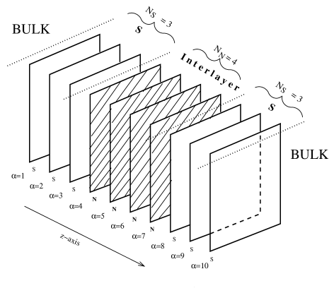
Our approach to quantum transport in ballistic junctions starts from a microscopic Hamiltonian defined on a simple cubic lattice (of lattice constant ). [34] It allows us to describe the transport for an arbitrary junction thickness, temperature, and barrier strength. Also, the geometry is such that the interlayer has the same width as the leads. For computational purposes, the infinite lattice which models the junction is divided into a self-consistent part and a bulk part, as shown in Fig. 1. A negative- Hubbard term is employed to model the real-space pairing of electrons due to a local instantaneous attractive interaction. [34, 37] The lattice Hamiltonian is given by
| (2) | |||||
where () creates (destroys) an electron of spin at site , is the hopping integral between nearest-neighbor sites and (energies are measured in units of ), which is taken to be the same in the and , and is the attractive Hubbard interaction for sites within the superconducting planes. The normal interlayer is described by the noninteracting part of the Hamiltonian (2), which is just a (clean) nearest-neighbor tight-binding model with a diagonal on-site potential . The potentials are not given a priori, but instead are calculated self-consistently by first determining the local electronic charge density and comparing it to the bulk charge density of the corresponding or layers. The imbalanced charge on each plane generates an electric field and thereby an electric potential. Summing the contributions from the charges on all other planes then yields the total local potential and the local potential energy shift . We now recalculate the charge density on each plane and iterate until is determined self-consistently (see below for a detailed description of the algorithm). The local potentials are largest near the interface, and decay as one approaches the bulk leads.
We use the Hartree-Fock approximation (HFA) for the interacting part of the Hamiltonian (2). This accounts for the superconductivity in the region in a way which is completely equivalent to a conventional BCS theory with an energy cutoff determined by the electronic bandwidth rather than by the phonon frequency. We choose half-filling and on the sites in the superconducting leads. The homogeneous bulk superconductor has a transition temperature and a zero-temperature order parameter . This yields a standard BCS gap ratio and a short
coherence length . The bulk critical current per unit area is , which is a bit higher than the current density determined by the Landau depairing velocity . This stems from the possibility of having gapless superconductivity in 3D at superfluid velocities slightly exceeding [42] (note that is direction-dependent for a cubic lattice at half-filling; we use the average value over the Fermi surface , appearing in the transport formulas, to compare our critical bulk supercurrent density to the expressions that assume a spherical Fermi surface and a density of particles ). The junction properties are studied here in the low-temperature limit at (the BCS gap is essentially temperature independent below ). At this temperature, the coherence length of the clean normal metal is . Since we do not consider inelastic scattering processes, the dephasing length is larger than . Therefore, determines the coherence properties of a single quasiparticle wave function inside the normal region.
The inhomogeneous superconductivity problem is solved by employing a Nambu-Gor’kov matrix formulation for the Green function between two lattice sites and at the Matsubara frequency ,
| (3) |
The corresponding local self-energy is given by the matrix
| (4) |
The diagonal and off-diagonal (i.e., normal and anomalous) Green functions are defined, respectively, as
| (5) | |||||
| (6) |
where denotes time-ordering in and . The self-energies and Green functions are coupled together through the Dyson equation,
| (8) | |||||
where the local approximation for the self-energy, , is assumed. In the HFA
for the attractive Hubbard model, the local self-energy is found from the local Green function by
| (9) |
and
| (10) |
The self-energy is time-independent because the interaction is instantaneous and we use the HFA (i.e., retardation effects in the superconductor are neglected). The noninteracting Green function, is diagonal in Nambu space, with an upper diagonal component given by
| (11) |
As all sites within a plane are identical, the self-energy need only be calculated once for each of the planes, while it is allowed to vary from plane to plane.
We work with Green functions represented in a mixed basis, which is defined by the two-dimensional momenta and the (discrete) -coordinate of the plane . This follows after the initial 3D problem is converted to a quasi-one-dimensional one [40] by performing a Fourier transformation within each plane (where the junction is translationally invariant) and retaining the real-space representation for the -direction of the inhomogeneity. For the local interaction treated in the HFA, computation of the Green function reduces to inverting an infinite block tridiagonal Hamiltonian matrix in real space. The Green functions are thereby evaluated as a matrix continued fraction (technical details are given elsewhere [38, 41]). The final solution is fully self-consistent in the order parameter inside the part of the junction comprised of the region and the first 30 planes inside the superconducting leads on each side of the interlayer (see Fig. 1). The self-consistent region is long enough because heals to its bulk value over just a few coherence lengths . Our Hamiltonian formulation of the problem and its solution by this Green function technique is equivalent to solving a discretized version of the Bogoliubov-de Gennes [39] (BdG) equations in a fully self-consistent manner, i.e. by determining the off-diagonal pairing potential in the BdG Hamiltonian [34] after each iteration until convergence is achieved. The tight-binding description of the electronic states also allows us to include an arbitrary band structure or unconventional pairing symmetry. [37]
In conjunction with the self-consistent solution of the superconducting part of the problem, we have to self-consistently solve the electrostatic problem. Although both the and are half-filled in most of our calculations (i.e., there is no mismatch in the Fermi wave vector), shifting the bottom of the band leads to a difference in their Fermi levels. This generates a redistribution of electrons around the interface when these are brought into contact. The resulting non-uniform electric field can be described by a potential (for simplicity, we use the label having in mind a discrete coordinate at a particular site ) which varies in the transition layer around the boundary with a thickness of . In the region the following condition is satisfied
| (12) |
in order to ensure a constant electrochemical potential throughout the system in equilibrium. The solution which satisfies this equation is usually simplified [28] to , where is a monotonic function of equal to for or for (this allows one to formulate quasiclassical equations in the region ). Here we treat the contact between the and in a fully microscopic fashion: starting from the Hamiltonian (2), a Fermi level mismatch , and assuming a screening length of a few lattice spacings, we find the charge redistribution around the contact, as well as the corresponding classical electrostatic potential generated by them. Thus, our technique can treat arbitrary spatial variation of the (lattice) Green functions, superconducting order parameter, and electrostatic potential. This includes the region , where we find a sharp increase of but never as sharp as the (unphysical) delta function.
Since our multilayer structure is translationally invariant in the transverse direction, each infinite plane has a uniform surface charge distribution which generates a homogeneous electric field pointing along the direction ( is the relative dielectric constant of the ionic lattice). The quantum-mechanical part of the electrostatic problem entails determining the local electron density (filling) at each site of a given plane
| (13) |
where is the in-plane kinetic energy for the transverse momentum , and is the two-dimensional tight-binding density of states on a square lattice (which is used for the sum over momenta parallel to the planes). The corresponding electric potential is determined classically from the “charge deviation” ( is the average filling in the bulk, or )
| (14) |
This must be summed over all planes to give the on-site potential . Therefore, the small induced charge imbalance satisfies (in a corresponding continuous system)
| (15) |
where is the total density of states at the chemical potential . This is integrated to give the distribution of the screened charge
| (16) |
which decays exponentially on a length scale set by the Debye screening length
| (17) |
Thus, the screening length is determined by and (for example, [31] and in high- superconductors). We choose which leads to . The self-consistency in the electrostatic problem is required because enters into the computation of the Green function as a diagonal potential in the Hamiltonian (2). The solution has converged when the potential is consistent with the charge distribution (13) determined from the Green function. Although this seems like a cumbersome computational task, the potential around the boundary barely changes when equilibrium Josephson current flows. Thus, the electrostatic part of the problem converges rapidly since the potential found in the solution at one phase gradient is a good initial guess for the iteration scheme at the next superconducting phase gradient.
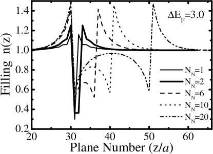
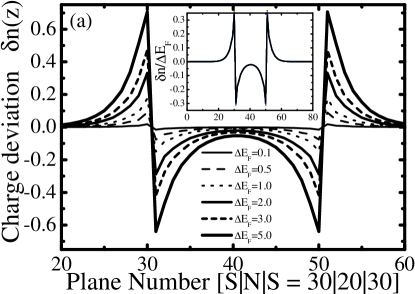
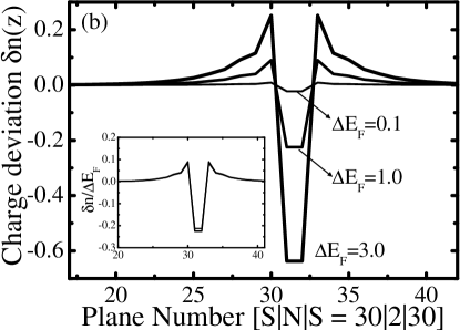
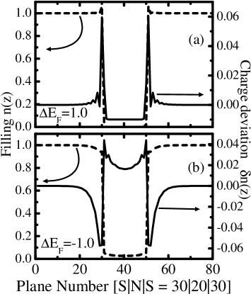
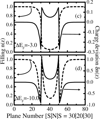
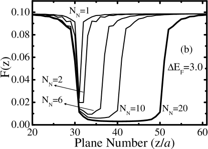
The density of electrons on each site in a given plane (at zero supercurrent) is plotted as a function of the junction thickness for in Fig. 2. The charge deviation from half-filling and the corresponding electrostatic potentials are (approximately) symmetric around the boundary for thick enough junctions, as shown in Fig. 3. Strictly speaking, only such symmetric distributions should be denoted “screened dipole layers”. For thinner junctions, where the screening of the excess charge does not heal to its equilibrium value, charge is depleted from the interlayer. The example of this behavior is the junction in the lower panel of Fig. 3. It leads to a non-monotonic resistance as a function of junction thickness at fixed (see Sec. IV). Thus, the charge effects become essential in short-coherence length superconducting junctions with thicknesses , which are encountered in high- grain boundaries. [31]
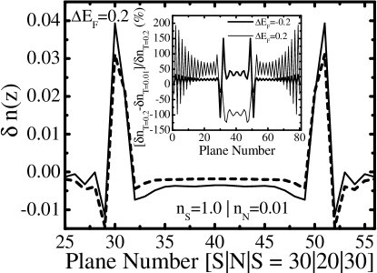
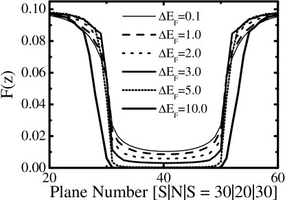
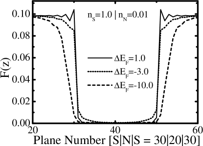
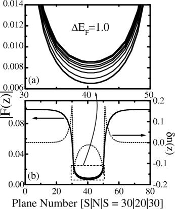
The interesting feature of the profiles for the half-filled and is that they can be approximately rescaled to a single reference distribution [set by ] after multiplying each of them by the ratio , as shown in the insets of Fig. 3. We believe this occurs because the noninteracting cubic density of states is nearly constant close to half filling. The scaling becomes essential in computing the properties of junctions with large since one can use the scaled potential profile computed at a smaller as the initial guess in the iteration procedure. Since the case has a higher degree of symmetry, we also perform calculations for (which approximates a doped semiconductor) in the normal region and half-filling in the superconductor. The result is shown in Fig. 4. Here the scaling of the distribution does not work as well (because the density of states has strong variation with energy). In addition, we find that the charge deviation is nonsymmetric, and yields a different for positive and negative [for symmetric filling the two distributions are simply related as ]. We also investigate the temperature dependence of the distributions of uncompensated charge for (the chemical potential in the bulk is for ) and at (which is close to ). In both cases and we find to be practically temperature independent (e.g., the change is at most around the boundary) for shown in the previous figure. This feature is exploited in Sec. IV to calculate the normal state resistance of our junctions from an imaginary axis computation of the charge and potential profile in the superconducting state. However, for and small a large change in the magnitude of is observed when going from to , as shown in Fig. 5. Similar phenomenon has been found in the recent Raman studies [32] which show a substantial change in the thickness of the charge accumulation layer at the interface between Nb and InAs, as Nb undergoes a superconducting transition and proximity effects develop in the InAs layer. This would point to a proximity effect influenced screening length, which cannot be seen in our local (Thomas-Fermi) screening theory containing only two parameters which determine : , which is fixed in our calculations, and the density of states which can be modified by the proximity effect. Our observation of the change in the charge concentration above () and below , without a palpable change in the screening properties, suggest that effects beyond the simple screening theory (e.g., nonlocal screening which becomes important in low filling cases [31]) probably have to be taken into account to understand this experiment.
III Self-consistent equilibrium properties of Junctions
We first provide an insight into the microscopic properties of these junctions which are determined by the proximity effect that affects the critical current (in non-self-consistent calculations such effects are taken into account only through some effective phenomenological suppression parameter [9]). They are encoded in the self-consistently computed variation of the amplitude and phase of the order parameter in the or pair amplitude in the . These are related to each other inside the by
| (18) |
where is obtained as the equal-time limit of the local anomalous Green function introduced in Sec. II
| (19) |
Although and are not directly measurable, they are important for understanding the superconductivity in inhomogeneous structures. Examples include the proximity effect in the and the depression of (compared to its bulk value) on the side of a boundary (“inverse proximity effect”). Since the critical current of the junction is determined by at the boundary, the study of throughout the junction gives direct insight into how self-consistency affects the transport properties (analytical approaches usually assume a step function for , which is applicable only for a limited range of junction parameters [12]). The non-zero value of inside the superconductor results from the attractive pairing interaction [which also gives rise to the non-zero order parameter ]. In the normal metal, and the gap vanishes, but can be non-zero due to the proximity effect. Therefore, it is more meaningful to plot , which is a continuous function throughout the junction. Inside the , should be understood as just . The superconducting
correlations are imparted to the region which is in contact with the . They are described quantitatively by the pair amplitude [43] (19). Because of the translational symmetry of the junction in the transverse direction, is constant within the plane, and changes from plane to plane along -axis. The scale over which changes exponentially from the interface to zero in the bulk of the is set by the normal metal coherence length . However, as the length diverges and the exponential decay of crosses over to a slower power-law decay (like at , inside a described by a Fermi liquid [44]).
Although this description of the proximity effect has been used since the early days of inhomogeneous superconductivity studies, [43] it is only recently that mesoscopic superconductivity [7] has established an explicit connection to a real-space picture of pairing correlations, provided by the phenomenon of (phase-coherent) Andreev reflection. [11] That is non-zero in a normal region is equivalent to saying that the electron and an Andreev reflected phase-conjugated hole maintain their single-particle phase coherence inside the . Technically, this interpretation follows directly from the expression for in terms of quasiparticle wave functions entering the BdG equations. [6] In other words, near the boundary, Andreev reflection mixes electron-like and hole-like quasiparticles in the same proportion in which they are mixed in the (where Bogoliubov quasiparticles are a mixture of electron-like and hole-like states with weights determined by the self-consistency condition) due to purely kinematic effects, since the interaction is absent in the . The definition of from Eqs. (3) and (19) in the second-quantized formalism, shows that such correlations can be interpreted alternatively as a condensate wave function leaking into the normal metal through the presence of evanescent Cooper pairs. [45] In the case of a Josephson junction, the overlap of two condensate wave functions provides a weak coupling between the superconducting leads, while insuring the global phase coherence and equilibrium current flow (i.e., the DC Josephson effect) for the time-independent phase difference between them. Thus, the two apparently different pictures of the Josephson effect in weak links (leakage of Cooper pairs versus Andreev reflection induced transfer of Cooper pairs) are in fact two facets of the same phenomenon.
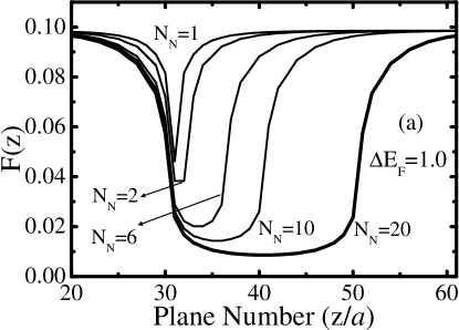
We first show two examples of computed self-consistently for vanishing supercurrent throughout the junction with . Figure 6 plots the scaling of with the junction thickness for the layers at the boundary being SDLs whose height is determined by or . The shape of evolves with the thickness, as well as with the height of the double-barrier. This second point is demonstrated in Fig. 7 where we fix and vary the strength of the SDL barrier. Here one would expect the evolution of toward a step function, which then justifies the use of rigid boundary conditions for strong enough scattering at the barriers. [12] However, we find a non-monotonic change in the shape of : the influence of a SDL on the order parameter is first reduced with increasing , but then leads to a depressed near the boundary for a strong charge imbalance generated by . Since our previous results for a junction having a strong on-site Coulomb potential, confined within a single plane, exhibit a step function like [38] , the effects observed here can be attributed to the finite spatial extent of the SDL. Moreover, we find that the step function (up to tiny oscillations near the boundary) for does develop in the special case of low filling in the region, like , and a small mismatch . A specific example of this behavior (compared to the case with the same parameters, but with a negative ) is shown in Fig. 8.
In the short junction case, the oscillations of on the scale of are observed for large enough . In this case, as discussed in the previous section, the junction is too thin for the distribution of charge to heal to its
equilibrium value. The charge depletion inside the brings it close to an insulating state. While oscillations on the scale of have been observed [34] in similar self-consistent calculations at (and attributed to the mesoscopic coherence of a single particle wave function), here it appears that they are a property of the superconducting interface which terminates at an “insulator” (this is also exhibited by a thick junction with small in Fig. 8). We have recently found such behavior, in its most pronounced form, in the case of junctions, with being a correlated insulator. [41] In the self-consistent calculations one can also observe how evolves, becoming smaller inside the region, as the phase change across the interlayer is increased and the Josephson current approaches . An example of such an effect due to self-consistency is shown in Fig. 9.
When self-consistency is satisfied, the phase of the order parameter is not a constant inside the leads (see also Sec. IV) because a phase gradient is needed to support the current in the ensuring current conservation throughout the junction. Thus, the change of phase from plane to plane has to be extracted from the self-consistent solution for . It can be expressed as the sum of a linear term and a “phase deviation” term
| (20) |
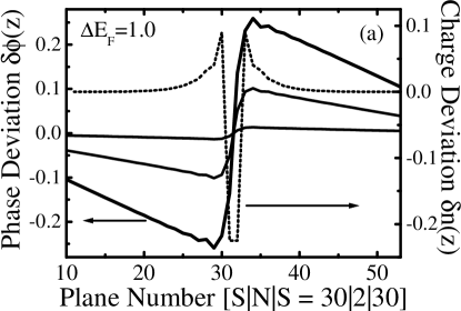
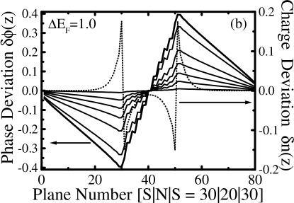
where the distance is measured from the origin along the -axis. The linear term is determined by the phase gradient which is set as the boundary condition in the bulk of the superconductor. The non-trivial information contained in is revealed by plotting . The overall phase increases smoothly and monotonically across the self-consistent region. We plot
for two different junction thicknesses with in Fig. 10. In general, oscillations of on the scale of are found for moderate and long enough junctions (). Oscillations, of both the phase and the order parameter, were found inside a long mesoscopic constriction in previous self-consistent calculations [34] at zero temperature (that gradually disappear with increasing ). Here we see the oscillations of at low temperature (but still ), while the corresponding (Fig. 6) does not oscillate.
IV Critical currents and characteristic voltages
In the self-consistent treatment, equilibrium supercurrent flows through the junction when the phase gradient exists in the bulk of the superconductor and a total phase change is established across the normal region. Therefore, we first find the solution for the bulk superconductor in both the absence of a supercurrent and in the presence of a supercurrent generated by a uniform variation in the order-parameter phase. The uniform bulk solution is then employed to provide the “boundary conditions” for the junction beyond the region where we determine properties self-consistently. Thus, our method does not require any assumptions about the boundary conditions at the interface between the barrier and the superconductor, which follow from the requirements of self-consistency. [38] We use current conservation as a stringent test of the achieved self-consistency in the solution for the Green function. Namely, the self-consistently determined ensures that Andreev reflection at each boundary generates supercurrent flow in the leads (besides being responsible for the proximity effect in
the discussed in Sec. II). Thus, the fulfillment of the self-consistency condition (18) means that the “source term” (on the right-hand side) vanishes in the equation of motion for the charge density operator
| (21) |
thereby recovering current continuity at every site ( is the current between two neighboring sites). When the current inside the superconductors is small, e.g., due to the geometrical dilution of a weak link with a junction area much smaller than , or when the junction resistance is dominated by a large interlayer resistance, [6, 12] one usually neglects the supercurrent flow and corresponding phase gradient in the bulk superconductor necessary to support it. Strictly speaking, such approaches violate current conservation. [35, 36] Inasmuch as our and layers have the same area, can be close to one for thin junctions with weak SDLs at small . In such cases, current flow affects appreciably the superconducting order parameter [i.e., both inside and outside of the , cf. Sec. III] and a self-consistent treatment becomes necessary (as is the case for the critical current of the bulk superconductor [42]). Because of the presence of a phase gradient inside the , the simple picture [1] of an equilibrium current being related to the phase difference between the left and right leads (where and are constant within the leads) is not applicable. Nevertheless, the solution for the current turns out
to be uniquely parameterized by a single quantity which can be taken as the phase change across the region [46] (the other option is the phase offset [35] which is related to the phase change by a nontrivial scale transformation). In a discrete model like ours, a convention has to be introduced on how this change is extracted from in Eq. (20). The thickness of the junction is defined to be the distance measured from the point , in the middle of the last plane on the left (at ) and the first adjacent plane (at ), to the middle point between the last and first plane on the right (cf. Fig. 1). Since is defined within the planes, we set to be the phase at , and equivalently for . The phase change across the barrier is then given by
| (22) |
for a junction of thickness . The current-phase relation is obtained by computing the current for a fixed bulk phase gradient and associating this value with the phase change across the region, which is extracted from the self-consistent pair amplitude . On the lattice, transport is described by the current across a link between two adjacent planes and . This current (per ) is obtained from the Green function connecting two neighboring planes as [38]
| (24) | |||||
The first iteration in our self-consistent algorithm usually gives a current which is smaller inside the than in the region. The iteration cycle is completed when the current is constant throughout the junction. The only approximation invoked here is the presence of a (typically small) discontinuity in the supercurrent at the
bulk-superconductor/self-consistent-superconductor interface. We find that the superconducting order has always healed to its bulk value at that point. However, sometimes there can be a jump in at this boundary when one nears the critical current. This discontinuity in the phase corresponds to a breakdown of current conservation at the this interface (it can become large for large and a thick junction, especially when one lies on the decreasing current side of the current-phase diagram). The critical current of the junction is reached when the planes with the lowest pair amplitude (which are located in the center of the ) can no longer support the necessary phase gradient to maintain current continuity.
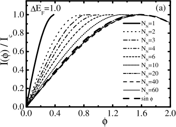
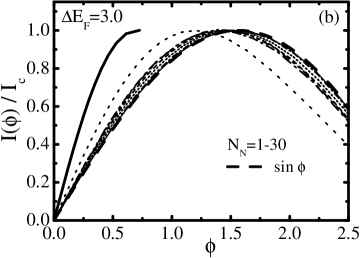
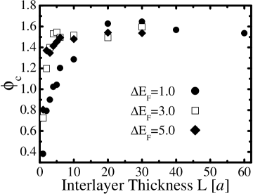
The scaling of the shape of the current-phase relation with the junction thickness is plotted in Fig. 11 for different . We find large deviations from the usual sinusoidal dependence for thin junctions and moderate heights of the SDL barriers. While in such cases (and at low temperatures) analytical predictions [4, 9, 20] also give non-sinusoidal , our “critical” phase change [] is always below the analytical prediction (Fig. 12), which can be attributed to the effects of self-consistency [35] (the other important distinction is that SDLs are spatially extended barriers). For thicker junctions, with high SDL barriers (and at high enough temperatures) the recovery of the usual junction current-phase relation is predicted. [9] Here we find a current-phase relation which is close to sinusoidal in the thick junction limit [(a) panel in Fig. 11], or in thin junctions with high SDL barriers [(b) panel in Fig. 11]. The corresponding critical current densities as a function of junction thickness are plotted in Fig. 13. For large , is non-monotonic because of the special role played by the barriers formed in the junctions with . When SDLs are completely screened inside the thick interlayers, the decay of current is determined just by the exponential decay of the proximity
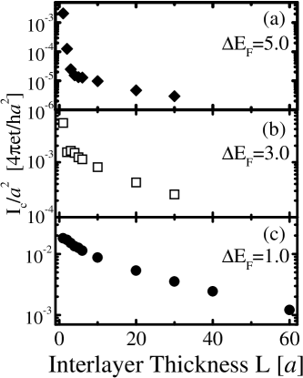
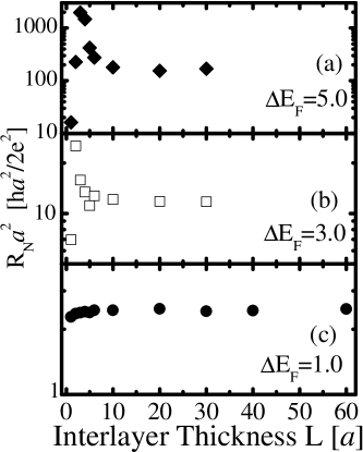
coupling between the leads through the clean normal interlayer (the resistance of these junctions is also practically independent of , see Fig. 14). For example, the characteristic decay length, extracted from fitting [12, 47] to for case in Fig. 13, is (with ). For larger , and long enough junctions to ensure monotonic decay of , appears to be shorter.
We use a Kubo linear response formalism to determine the normal state resistance . Kubo theory is formulated in terms of the non-local conductivity tensor
| (25) |
which relates the current density to the electric field through a non-local Ohm’s law (at finite frequency these are the respective Fourier components). Its physical meaning is obvious—it gives the current response at due to an electric field at . Although an external electric field induces charges (and corresponding potentials) to linear order, the linear transport properties, like , are found as the response to an external field only. This is because the current response to this inhomogeneous field (external + induced) is already beyond linear response. [49] Thus, only equilibrium screening has to be included in the Hamiltonian used to compute the Green function entering below. [50] This makes it possible to use the potential generated by the charge distributions (discussed in Sec. II), which is computed from the imaginary axis calculations, as an on-site fixed potential in the equilibrium Hamiltonian (2). In this way
the potential of the SDLs enters the resistance calculation through the Green functions in Eq. (31) computed by real-axis analytic continuation. The DC conductance of the sample of volume is expressed through as
| (26) | |||||
| (27) |
where is the local field inside the sample and is the externally applied voltage. Because of current conservation requirements on the form of [48] , it is possible to use arbitrary electric field factors in Eq. (26) [including a homogeneous field ].
Since our system is effectively one-dimensional (in real space) we need to calculate the longitudinal component in the -direction (perpendicular to the uniform planes) of . In a lattice model like ours, the relevant component of this tensor, , is given by (neglecting vertex corrections)
| (31) | |||||
where is the Fermi-Dirac distribution function. We first find the self-consistent solutions for the system in the normal state, with no current flowing, by setting the order parameter to zero on all planes. These solutions are then employed to calculate the Kubo tensor (31). The self-energy of the planes outside the interlayer contains only a constant real part, as the calculation is carried out within the HFA. Given the set of local self-energies, the Green functions which couple any two planes are readily found, for any momentum parallel to the planes.
The conductance (per unit area ) of the lattice system is obtained from the discretized version of (26)
| (32) |
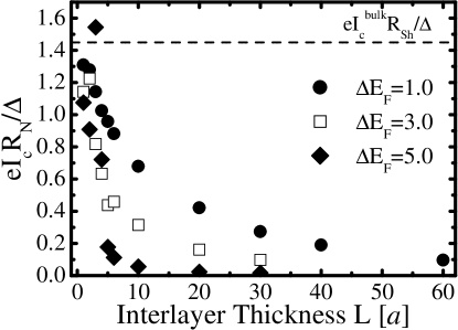
as the sum of the components of the non-local Kubo conductivity tensor. Thus, although one can find the inhomogeneous field [38] (across all links connecting planes and ) by inverting the discretized version of Eq. (25), for a constant throughout the system, the final expression for the conductance does not contain this field. The normal state resistances calculated in this framework are plotted in Fig. 14. In thin junctions and for large enough , a charge depletion layer arises inside the which leads to a non-monotonic behavior of (e.g., increases sharply for and , or and ). On the other hand, for small enough the conductance is only slightly changed from the Sharvin point contact conductance [51] of a ballistic junction per unit area , . Therefore, comparison of Fig. 13 and Fig. 14 shows that the SDL depresses the current substantially, while only weakly increasing the resistance. This reduces the product, plotted in Fig. 15, thus showing that charge accumulation layers are detrimental to junction performance in electronics circuits. This is further confirmed by the fact that in most of these junction is below the product of the bulk critical current and the Sharvin point contact resistance , which is the upper limit of the characteristic voltage in a clean weak link (the junction made of the same leads as studied here, but with a dirty interlayer, exhibits , for some range of parameters [41]). Therefore, the SDL induced scattering on a boundary is one of the mechanisms which can account for the low products observed in experiments [33] on nominally ballistic short junctions (where , being determined by the thin charge layer only, does not scale with just like what happens in ballistic conductors). One way to test this conjecture is to use electron holography to map out
the charge profile near the SN interface of these ballistic junctions.
V Conclusions
We have studied the influence of a charge imbalance, that arises at the boundary between a short coherence length superconductor and a normal metal (due to Fermi energy mismatch) on the equilibrium properties of a Josephson junction (where the and layers are of the same width). The screening length is large enough to generate a spatially extended charge redistribution that allows us to examine the interplay between the charge layer formation and superconductivity (characterized by the coherence length comparable to the screening length) near the boundary and in the interlayer. This resembles the charge redistribution on the grain boundaries of a high- superconductor. At half-filling in both the and , the charge distribution and its potential are symmetric (screened dipole layer), and can be rescaled to a single one determined by some reference Fermi level mismatch . When charge concentration in the is a hundred times smaller than in the , we find a proximity effect induced change in the charge redistribution generated by a small Fermi level mismatch upon moving from (where is of the order of ) to .
The step-function-like order parameter (which is used in non-self-consistent approaches) is recovered only in the case of a low charge density in the (compared to the filling in the ) and a small mismatch . The junction exhibits unusual properties when its thickness is comparable to the screening length. While the charge layer leads to a depression of the order parameter near the boundary, and thereby the junction critical current, it influences the normal state resistance in a much weaker fashion. Therefore, the product, relevant for digital electronics application, is reduced. This points out that such space-charge layers should be avoided to optimize junction performance and increase the critical current in high- superconductors. [52]
Acknowledgements
We are grateful to the Office of Naval Research for financial support from the grant number N00014-99-1-0328. Real-axis analytic continuation calculations were partially supported by HPC time from the Arctic Region Supercomputer Center. We have benefited from the useful discussions with A. Brinkman, J. Ketterson, T. Klapwijk, K. K. Likharev, J. Mannhart, I. Nevirkovets, N. Newman, I. V. Roshchin, J. Rowell, S. Tolpygo, and T. van Duzer.
REFERENCES
- [1] B. D. Josephson, Phys. Lett. 1, 251 (1962).
- [2] T. van Duzer and C. W. Turner, Priciples of Superconducting Devices and Circuits (2nd ed., Prentice Hall, Upper Saddle River, 1999).
- [3] A. Kastalsky, A.W. Kleinsasser, L.H. Greene, R. Bhat, F.P. Milliken, and J.P. Harvison, Phys. Rev. Lett. 67, 3026 (1991); A. W. Kleinssaser and A. Kastalsky, Phys. Rev. B 47, 8361 (1993).
- [4] A. Brinkman and A. A. Golubov, Phys. Rev. B 61, 11 297 (2000).
- [5] A. F. Volkov, Phys. Rev. Lett. 74, 4730 (1995).
- [6] C. W. J. Beenakker, Rev. of Mod. Phys. 69, 731 (1997).
- [7] Special issue of Superlattices and Microstructures, 25 No. 5/6 (1999).
- [8] M. Maezawa and A. Shoji, Appl. Phys. Lett. 70, 3603 (1997).
- [9] For a review see: M. Yu. Kupriyanov, A. Brinkman, A. A. Golubov, M. Siegel, H. Rogalla, Physica C 326-327, 16 (1999).
- [10] A. Brinkman, A. A. Golubov, H. Rogalla, and M. Kupriyanov, Supercond. Sci. Technol. 12, 893 (1999); D. Balashov, F.-Im. Buchholz, H. Schulze, M. I. Khabipov, R. Dolata, M. Yu. Kupriyanov, and J. Niemeyer, Supercond. Sci. Technol. 12, 244 (2000).
- [11] A. F. Andreev, Zh. Eksp. Teor. Fiz. 46, 1823 (1964) [Sov. Phys. JETP 18, 1228 (1964)].
- [12] K. K. Likharev, Rev. Mod. Phys. 51, 101 (1979).
- [13] M. B. Ketchen, IEEE Trans. Magn. 27, 2916 (1991).
- [14] K. K. Likharev and V. K. Semenov, IEEE Trans. Appl. Supercond. 1, 1 (1991).
- [15] M. Gurvitch, M. A. Washington, and H. A. Huggins, Appl. Phys. Lett. 42, 472 (1983).
- [16] A. W. Kleinsasser, A. C. Callegari, B. D. Hunt, C. Rogers, R. Tiberio, and R. A. Buhrman, IEEE Trans. Magn. 17, 307 (1981).
- [17] A. Zehnder, Ph. Lerch, S. P. Zhao, Th. Nussbaumer, E. C. Kirk, and H. R. Ott, Phys. Rev. B 59, 8875 (1999).
- [18] L. G. Aslamasov, A. I. Larkin, and Yu. N. Ovchinnikov, Sov. Phys. JETP 28, 171 (1969).
- [19] W. Belzig, F.K. Wilhelm, C. Bruder, G. Schön, and A.D. Zaikin, Superlattices and Microstructures 25, 1251 (1999).
- [20] M. Yu. Kupriyanov and V. F. Lukichev, Sov. Phys. JETP 67, 1163 (1988).
- [21] G. E. Blonder, M. Tinkham, and T. M. Klapwijk, Phys. Rev. B 25, 4515 (1982).
- [22] A. Furusaki, H. Takayanagi, and M. Tsukada, Phys. Rev. B 45, 10 563 (1992).
- [23] A. Chrestin, T. Matsuyama, and U. Merkt, Phys. Rev. B 59, 498 (1994).
- [24] G. Johansson, E. N. Bratus’, V. S. Shumeiko, and G. Wendin, Phys. Rev. B 60, 1382 (1999).
- [25] I. P. Nevirkovets and S. E. Shafranjuk, Phys. Rev. B 59, 1311 (1999).
- [26] M.A.M. Gijs and G.E.W. Bauer, Adv. Phys. 46, 286 (1997), and references therein.
- [27] V. K. Dugaev, V. I. Litvinov, and P. P. Petrov, Phys. Rev. B 52, 5306 (1995).
- [28] A. V. Zaitsev, Zh. Eksp. Teor. Fiz. 86, 1742 [Sov. Phys. JETP 59, 1015 (1985)].
- [29] K. A. Delin and A. W. Kleinsasser, Supercond. Sci. Technol. 9, 227 (1996).
- [30] J. Mannhart and H. Hilgenkamp, Appl. Phys. Lett. 73, 265 (1998).
- [31] A. Gurevich and E. A. Pashitskii, Phys. Rev. B 57, 13 878 (1998).
- [32] I. V. Roshchin, A. C. Abeyta, L. H. Greene, T. A. Tanzer, J. F. Dorsten, P. W. Bohn, S.-W. Han, P. F. Miceli, and J. F. Klem, unpublished; I. V. Roshchin, Ph.D. thesis, Electronic and optical properties of thin-film superconductors and superconductor-semiconductor interfaces, Department of Physics, University of Illinois at Urbana-Champaign, Urbana (2000); L. H. Greene, J. F. Dorsten, I. V. Roschchin, A. C. Abeyta, T. A. Tanzer, G. Kuchler, W. L. Feldmann, P. W. Bohn, Czech. J. Phys. 46, 3115 (1996).
- [33] J.P. Heida, B.J. van Wees, T.M. Klapwijk, and G. Borghs, Phys. Rev. B 60, 13 135 (1999), and references therein.
- [34] A. Levy-Yeyati, A. Martn-Rodero, and F. J. Garca-Vidal, Phys. Rev. B 51, 3743 (1995); J. C. Cuevas, A. Martn-Rodero, and A. Levy Yeyati, Phys. Rev. B 54, 7366 (1996).
- [35] F. Sols and J. Ferrer, Phys. Rev. B 49, 15913 (1994).
- [36] R. A. Reidel, L.-F. Chang, and F. Bagwell, Phys. Rev. B 54, 16 082 (1996).
- [37] A. M. Martin and J. F. Annett, in Ref. [7].
- [38] P. Miller and J. K. Freericks, J. Phys.: Condens. Matter. 13, 3187 (2001).
- [39] P. G. de Gennes, Superconductivity of Metals and Alloys (Addison-Wesley, 1966).
- [40] M. Potthoff and W. Nolting, Phys. Rev. B 59, 2549 (1999).
- [41] J. K. Freericks, B. K. Nikolić, and P. Miller, cond-mat/0103067.
- [42] J. Bardeen, Rev. Mod. Phys. 34, 667 (1962).
- [43] G. Deutscher and P.G. De Gennes, in Superconductivity, ed. by R.D. Parks, (Marcel Dekker, New York, 1969), Vol. II, p. 1005.
- [44] D. S. Falk, Phys. Rev. 132, 1576 (1963).
- [45] G. B. Lesovik, T. Martin, and G. Blatter, cond-mat/0009193.
- [46] M. Yu. Kupriyanov, Pis’ma Zh. Eksp. Teor. Fiz. 56, 414 (1992) [JETP Lett. 56, 399 (1992)].
- [47] A. W. Kleinsasser and T. N. Jackson, Phys. Rev. B 42, R8716 (1990).
- [48] C. L. Kane, R. A. Serota, and P. A. Lee, Phys. Rev. B 37, 6701 (1988).
- [49] B. K. Nikolić and P. B. Allen, Phys. Rev. B 60, 3963 (1999).
- [50] A. D. Stone, in Mesoscopic Quantum Physics, edited by E. Akkermans, J.-L. Pichard, and J. Zinn-Justin, Les Houches, Session LXI, 1994 (North-Holland, Amsterdam, 1995)..
- [51] Yu. V. Sharvin, Zh. Eksp. Teor. Phys. 48, 984 (1965) [Sov. Phys. JETP 21, 655 (1965)].
- [52] A. Scheml, B. Goetz, R. R. Schulz, C. W. Schneider, H. Bielefeldt, H. Hilgenkamp, and J. Mannhart, Europhys. Lett. 47, 110 (1999); G. Hammerl, A. Schmehl, R. R. Schulz, B. Goetz, H. Bielefeldt, C. W. Schneider, H. Hilgenkamp, and J. Mannhart, Nature 407, 162 (2000).