Role of doped layers in dephasing of 2D electrons in quantum well structures
Abstract
The temperature and gate voltage dependences of the phase breaking time are studied experimentally in GaAs/InGaAs heterostructures with single quantum well. It is shown that appearance of states at the Fermi energy in the doped layers leads to a significant decrease of the phase breaking time of the carriers in quantum well and to saturation of the phase breaking time at low temperature.
pacs:
73.20.Fz, 73.61.EyInelasticity of electron-electron interaction is the main mechanism of dephasing of the electron wave function in low-dimensional systems at low temperature. Whereas the theory predicts divergence of the phase breaking time with decreasing temperature,Tf an unexpected saturation of at low temperatures has been experimentally found in one- and two-dimensional structures.r1 ; r2 These observations rekindle a particular interest to dephasing.
In order to perform transport experiments, a - or modulation doped layer is arranged in semiconductor heterostructures. Usually the doped layer is spaced from the quantum well, all carriers leave the impurities and pass into the quantum well. In some cases a fraction of the carriers remain in the doped layer. As a rule, these carriers do not contribute to the DC conductivity because they are localized in fluctuations of long range potential. In other words, the percolation threshold of doped layer is above the Fermi level. In this paper we demonstrate that presence of the carriers and/or empty states in doped layer at the Fermi energy can contribute to dephasing and its temperature dependence.
The main method of experimental determination of the phase breaking time is an analysis of the low-field negative magnetoresistance, resulting from destruction of the interference quantum correction to the conductivity. We have measured the negative magnetoresistance in a single-well gated heterostructures GaAs/InxGa1-xAs. The heterostructures were grown by metal-organic vapor-phase epitaxy on a semiinsulator GaAs substrate. They consist of -mkm-thick undoped GaAs epilayer, a Sn layer, a 60-Å spacer of undoped GaAs, a 80-Å In0.2Ga0.8As well, a 60-Å spacer of undoped GaAs, a Sn layer, and a 3000-Å cap layer of undoped GaAs. The samples were mesa etched into standard Hall bridges and then Al gate electrode was deposited onto the cap layer by thermal evaporation. The measurements were performed in the temperature range K at magnetic field up to 6 T. The discrete at low-field measurements was T. The electron density was found from the Hall effect and from the Shubnikov-de Haas oscillations. These values coincide with an accuracy of 5% over the entire gate-voltage range.
Varying the gate voltage from to V we changed the electron density in quantum well from to cm-2 and the conductivity from to Ohm-1. The low-field magnetoconductivity for two gate voltages is shown in Fig. 1. To determine the phase breaking time we have used the standard procedure of fitting of the low-field magnetoconductivity to the Hikami expression r3
| (1) | |||||
where , , is the mean-free path, is the momentum relaxation time, is the digamma function, and is equal to unity. This expression was obtained within the diffusion approximation. Nevertheless, as shown in Ref. r4, , with less than unity it can be used for analysis of the experimental data even beyond the diffusion approximation, giving the value of close to true one. The results of fitting carried out in two magnetic field ranges are presented in Fig. 1. One can see that the values of fitting parameters somewhat depend on the magnetic field range. However, the difference in does not exceed %. The value of is lower than unity and lies within the interval . This is result of the fact that in the structure investigated the ratio is not low enough:r4 .
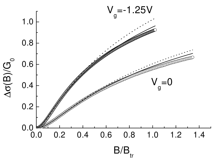
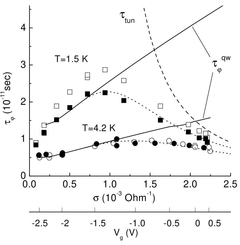
Figure 2 shows the conductivity dependence of for two temperatures. One can see that -versus- plot exhibits maximum: increases with increasing conductivity while Ohm-1 and decreases at higher values. Qualitatively this behavior is independent of the fitting range. The maximum is more pronounced at lower temperature.
Nonmonotonic conductivity dependence of is in conflict with the theoretical prediction. In 2D systems the main phase breaking mechanism at low temperature is inelasticity of the electron-electron interaction and the phase breaking time has to increase monotonically with :Tf
| (2) |
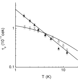
As is seen from Fig. 2 the conductivity dependence of is close to the theoretical one only when Ohm-1, but significantly deviates for higher . In addition, the increase of leads to changing in the temperature dependence of (see Fig. 3). When Ohm-1, the temperature dependence of is close to predicted theoretically. At higher , the -versus- plot shows the saturation at low temperature.
To interpret the experimental temperature and conductivity dependences of , let us first analyze the variation of electron density in the quantum well with the gate voltage [see Fig. 4(a)]. The total electron density in a gated structure has to be given by the simple expression , where is the gate–2D channel capacity per centimeter squared. Straight line in Fig. 4(a) represents this dependence obtained with as fitting parameter and , where Å is the cap-layer thickness, . One can see that over the range of from to V the experimental data are close to the calculated dependence, whereas at V the electron density in the quantum well is less, than the total density .
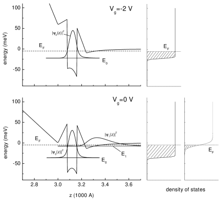
Such a behavior can be understood from inspection of Fig. 5, which presents the energy diagram of the structure investigated for two gate voltages. Selfconsistent calculation shows that at V there are only the states located in the quantum well (upper panels). At V the states located in -layer appear (lower panels). However, it should be borne in mind that the strong potential fluctuations in -layer leads to formation of the tail in density of these states. At low electron density in -layer, when the Fermi level lies within the tail, the electrons are localized in potential fluctuations and, thus, do not contribute to the structure conductivity. The absence of both magnetic field dependence of the Hall coefficient and positive magnetoresistance in wide range of magnetic field shows that this situation occurs in our structures while cm-2.
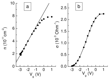
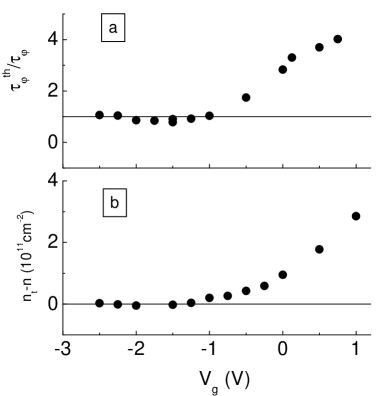
Now we are in position to put together the gate voltage dependences of the phase breaking time and those of the electron density in -layer. Figure 6 shows the ratio as function of , where has been found from Eq. (2) with the use of experimental -versus- dependence presented in Fig. 4(b). It is clearly seen that the experimental values of are close to theoretical ones, i.e., , when there are no electrons in -layer ( V) and become to be significantly less when carriers appear therein ( V). Thus, an additional mechanism of phase breaking for electrons in the quantum well arises when the -layer is being populated.
One of such mechanisms can be associated with tunneling. Indeed, appearance of electrons in -layer means arising of empty states at the Fermi energy therein, and, as sequence, tunneling of electrons between quantum well and -layer. In this case, an electron moving over closed paths (just they determine the interference quantum correction) spend some time within the -layer. Due to low value of local conductivity in -layer, the electron fast losses the phase memory therein.111Strictly speaking, the phase breaking mechanisms in doped layers, where electrons occupy the states in the tail of density of states, are the subject of additional study, but it seems no wonder that dephasing in these layers occurs faster than in quantum well. If the phase breaking time in -layer is much shorter than both the tunneling time and the phase breaking time in quantum well , the effective phase breaking time will be given by simple expression
| (3) |
Let us analyze our experimental results from this point of view. We can find the gate-voltage dependence of and thus the conductivity one from Eq. (3) using calculated from Eq. (2) and the experimental values of for K. The results presented in Fig. 2 by dashed line was obtained with determined from the fitting within the magnetic field range . It is seen that sharply decreases when the conductivity increases. Such a behavior is transparent. The tunneling probability is proportional to the density of final states. In our case the final states are the states in the tail of the density of states of -layer, therefore their density at the Fermi energy increases when increases (see Fig. 5).
Since the tunneling is temperature independent process, Eq. (3) with the -versus- dependence found above has to describe the experimental gate-voltage dependence of for any temperatures. Really, as is seen from Fig. 2 the results for K are very close to calculated curve.
The tunneling has to change the temperature dependence of also. Because increases with the temperature decrease as , the effective phase breaking time has to saturate at low temperature. In Fig. 3 the temperature dependences of found from Eq. (3) with calculated from Eq. (2) and determined above are presented. Good agreement between the calculated and experimental results shows that this model naturally describes the low-temperature saturation of .
Thus, taking into consideration the electron tunneling between quantum well and -layer we have explained both the gate-voltage and temperature dependences of phase breaking time.
Another possible mechanism of phase breaking for systems where carriers occur not only in the quantum well is their interaction with carriers in doped layer. Inelasticity of this interaction can be of importance. High efficiency of such interaction can be result of exciting of local plasmon modes in -layers, for example. We do not know the papers where inelasticity of the interaction between electrons in quantum well and in doped layer was taken into account.
In conclusion, the study of weak localization in gated structures shows that appearance of carriers in doped layer leads to decreasing of the phase breaking time and changing in the conductivity and temperature dependences of . It should be mentioned that the - or modulation doped layers are arranged in all the heterostructures suitable for transport measurements, to create the carriers in quantum well. The mechanisms discussed above can be important for phase breaking, even though the doped layers do not contribute to the conductivity.
Acknowledgment
This work was supported in part by the RFBR through Grants No. 00-02-16215, No. 01-02-06471, and No. 01-02-17003, the Program University of Russia through Grants No. 990409 and No. 990425, the CRDF through Award No. REC-005, and the Russian Program Physics of Solid State Nanostructures.
References
- (1) B. L. Altshuler and A. G. Aronov, in Electron - Electron Interaction in Disordered Systems, edited by A. L. Efros and M. Pollak, (North Holland, Amsterdam, 1985) p.1.
- (2) P. Mohanty, E. M. Q. Jarivala, and R. A. Webb, Phys. Rev. Lett. 78, 3366 (1997).
- (3) W. Poirier, D. Mailly, and M. Sanquer, preprint available at http://xxx.lanl.gov/abs/cond-mat/9706287.
- (4) S. Hikami, A. Larkin, and Y. Nagaoka, Prog. Theor. Phys. 63, 707 (1980).
- (5) G. M. Minkov, A. V. Germanenko, V. A. Larionova, S. A. Negashev, and I. V. Gornyi, Phys. Rev. B 61, 13164 (2000).