[
Multiwalled carbon nanotube: Luttinger liquid or not?
Abstract
We have measured curves of multiwalled carbon nanotubes using end contacts. At low voltages, the tunneling conductance obeys non-Ohmic power law, which is predicted both by the Luttinger liquid and the environment-quantum-fluctuation theories. However, at higher voltages we observe a crossover to Ohm’s law with a Coulomb-blockade offset, which agrees with the environment-quantum-fluctuation theory, but cannot be explained by the Luttinger-liquid theory. From the high-voltage tunneling conductance we determine the transmission line parameters of the nanotubes.
pacs:
PACS numbers: 74.50.+r, 73.23.-b, 73.23.Hk]
Metallic carbon nanotubes are considered as outstanding realizations of strongly interacting, one-dimensional electron systems, i.e. Luttinger liquids (LL) [1, 2, 3]. A Luttinger liquid is a paramagnetic metal without Fermi-liquid quasiparticles. Its basic charged excitations are plasmons which can be viewed as propagating electrodynamic modes in a similar fashion as in any regular transmission line. Experimental evidence for LL behavior has recently been observed in single walled carbon nanotubes [4] as well as in multiwalled tubes (MWNT) [5]. The transmission line analogy, in turn, facilitates the connection of LL theory to the environment-quantum-fluctuation (EQF) theory [6, 7]. This theory has been successful in explaining Coulomb blockade in normal tunnel junctions [7]. Unlike the LL model, the EQF theory incorporates various factors, which makes it much more amenable to detailed experimental comparison, especially in the case of resistive transmission lines.
In this paper we present experimental results on the -curves for four metallic, arc-discharge-grown MWNTs. We analyze our results using both the EQF analysis [6, 7] as well as the standard LL formulas [8, 9]. At small voltages both of these approaches predict for -curves a power law , which is also supported by the experiments yielding . At large voltages we find that only the EQF theory is applicable and obtain for the high frequency impedance k. From the values of and we can independently determine the kinetic inductance of the nanotubes and obtain consistent values of nH/m.
A multiwalled nanotube consists of several concentric nanotubes. About one third of the tubes are expected to be metallic with quite large inter-layer capacitance. According to our analysis, the large capacitance connects the inductive as well the resistive components of separate tubes in parallel. All metallic tubes take part in the conduction at high frequencies, in contrast to the Aharonov-Bohm experiments of Ref. [5] where only the outermost layer contributed to the dc-resistance. The total electron density of a MWNT is proportional to , the number of metallic layers, and in each channel the Fermi velocity of 1D electron gas is m/s. Here is the effective mass of an electron, and we have taken into account the fact that each metallic layer has four independent 1D conduction channels.
A metallic nanotube, placed on a silicon substrate between metallic contact lines, can be viewed as an inner conductor of a transmission line whose outer conductor is formed by nearby metallic bodies. The capacitance per unit length of the line is ln. Here is the dielectric constant of the medium between the conductors, is the outer radius of the nanotube, and is a distance from a metallic ground. The current carriers of the nanotube occupy 1D conduction bands and, in contrast to the carriers in metallic wires, they have a low total density , resulting in a large kinetic energy stored in the current flow. Therefore, the magnetic inductance ln, which is usually relevant for transmission lines, has to be replaced by the kinetic inductance , since . In addition, for a 1D plasmon in a nanotube the inverse compressibility of the neutral Fermi gas becomes comparable to the electrostatic inverse compressibility of the transmission line geometry. This can be taken into account by renormalization of the nanotube capacitance into :
| (1) |
Hence, the plasmon velocity is
| (2) |
and in the expression for the line impedance ,
| (3) |
is the electrochemical (not only electric) potential difference, and is the quantum resistance.
In the above classical electrodynamic analysis the 1D plasmon modes are the only excitations of the nanotube transmission line. The LL model for an infinitely long MWNT [8, 9] recovers the electrodynamic plasmon mode with given by Eq. (2) (cf. the expression after Eq. (4) in Ref. [8]). But in addition to the plasmon mode, the Luttinger liquid has charge-neutral modes (a spin wave among them), which propagate with the velocity different from and keep the total charge density constant. The Coulomb interaction, measured by the difference of from unity, suppresses the single electron density of state (DOS) near the Fermi level. The DOS is given by the Fourier component of the electron Green’s function ( is the electron operator) and is probed by the curve: . At low energies , where for an end-contacted infinitely long MWNT [9, 10]
| (4) |
In the limit of large or no-interaction , the -characteristics of a MWNT approach Ohm’s law (), the Luttinger liquid turns into a Fermi-liquid.
Another approach, the EQF theory, considers the effects of environment quantum fluctuations on -characteristics under the conditions of Coulomb blockade. A non-resistive, infinitely long nanotube acts as a dissipative environment, i.e., as a heat bath with which the tunneling electron can exchange energy [6, 7]. The energy exchange is characterized by the function , which is a Fourier component of the correlator , where is the operator of the phase. At , is proportional to the second derivative of the current: . In the Coulomb blockade regime, i.e. when the voltage bias is less than , where is the capacitance of the tunnel contact, the EQF theory predicts that and with . Using the impedance of the nanotube, this yields the same power law as the LL theory in the large limit. This fact, pointed out in Ref. [10], is not accidental. In the LL picture the current is suppressed because there are no single electron quasiparticles, and the charge is transported by bosonic modes (plasmons). Although in a junction between 3D wires there are single-electron states available (in contrast to 1D), a tunneling electron at has not enough energy to get into them. As a result, the charge is transported again with 1D plasmons, which have similar properties for 1D and thin 3D wires.
On the other hand, one should expect a similarity between and , since both the operators, and , which define these two functions, are creation operators for the charge . But if the exponents and for the conductance coincide, the exponents and for and , respectively, differ by one. One can show [11], however, that similar relations connect the - and -exponents with the impedance: and . But due to charge-neutral modes, which were not considered in the EQF theory, the nanotube impedance differs in the LL theory from the impedance given by Eq. (3): . The difference in the impedance compensates the difference in the relations connecting and with the conductance, and eventually in the large limit both the theories predict the same exponent.
But the two approaches differ in their predictions for high voltages. According to the EQF theory the power law is only valid in the Coulomb blockade regime . The relevant frequency in this inequality corresponds to the environment mode excited by a tunneling event; in our experiments this means frequencies up to about 20 THz. At high frequencies and voltages the environmental impedance is shunted by tunnel junction capacitance and becomes . Then the EQF theory gives the formula [7]
| (5) |
This high-voltage asymptotics, characterized by the Coulomb offset and the “tail” voltage was experimentally studied and discussed by Wahlgren et al., and Penttilä et al. within the horizon picture [12, 13]. In contrast to the EQF, in the LL approach the capacitance of the tunneling contact is absent, and therefore this approach does not predict a crossover to the “tail” asymptotics given by Eq. (5).
A summary of our four nanotube samples, each with a diameter of about 15 nm, is presented in Table I. For contact, we employed gold electrodes which were evaporated either prior to or after the deposition of nanotubes. Deposition of nanotubes was done as described in Ref. [14]. Mapping of nanotubes with respect to alignment marks as well as AFM micromanipulation was performed using Park Scientific Instruments Autoprobe CP. Chrome or titanium (2-3 nm layer) was employed as an attachment layer before evaporating gold. Vacuum brazing at 700 C for 30 sec was employed to lower the contact resistance in samples T1-T3. On the dilution refrigerator, the samples were mounted inside a tight copper enclosure and the measurement leads were filtered using 0.5 m of Thermocoax cable.
Tunnel junction capacitances aF and resistances k (neglecting the tube resistance) were determined from asymptotic behavior by fitting Eq. (4) to the measured -curves. Owing to their relatively large size, the contacts to the nanotube are not ideal and may cause a small uncertainty in the interpretation of the values. Namely, the EQF theory and the LL model in the strong interaction and limit predict two times smaller values for the bulk than for the end contact [7, 8, 9].
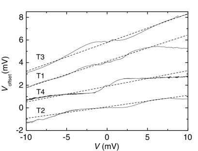
Fig. 1 illustrates the low-voltage -curve of all four samples T1-T4. We are plotting the quantity vs. , which in the case of a power law yields a straight line with the slope . Only slight deviation of linear behavior is seen at low voltages in Fig. 1. This indicates that the Coulomb blockade of the island is rather weakly seen (except in T4). The linear behavior also implies that the two tunnel junctions become independent. At voltages mV, in spite of the additional wiggles, slight tendency toward saturation is observed in the data. This is consistent with the EQF picture, which predicts that at high voltages must gradually approach to a -dependent constant. By fitting a straight line through each data set at mV, we obtain (Table 1). Using Eqs. (2) and (3) we obtain nH/m for the kinetic inductance. Capacitance for the nanotube aF/m is estimated using the average of where we employ the total tube length for scaling.
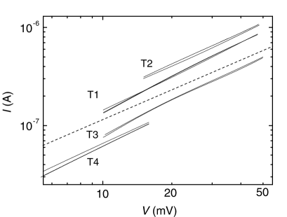
Fig. 2 displays -curves measured at large voltages. In order to facilitate a direct comparison with the power-law dependence, we have plotted our results on a log-log scale. Our data are rather close to a single power law with small but, at larger values of (samples T1 and T3), there is a gradual approach toward a linear law as expected for a single junction in a resistive environment. Thus both figures give evidence that the environmental (EQF) theory is better suited for the analysis at high voltages. In fact, also the saturation observed by Bockrath et. al. [4] can be explained by asymptotic approach toward Ohm’s law.
The plasma resonances, which one expects in finite nanotubes, are washed away in our samples. This gives a lower limit for the resistivity of the line, . On the other hand, the -line model works over our voltage range, i.e. , which results in an upper limit for of the order of 1 km (at 1 mV). For comparison, from the two-terminal resistance measurements we estimate that km for our tubes at DC [15].
One may argue that the poor agreement of the LL picture with the high-voltage part of the curves could be reconciliated by including the junction capacitance into the impedance, as is done in the EQF theory. There is, however, a conceptual problem to do it. The density of state is expected to be a bulk property and, therefore, independent of . Moreover, inclusion of into the impedance, which determines , does not help to match the LL picture with experimental results. The capacitance short circuits the environment impedance, and should decrease with , like in the EQF theory. But since , in contrast the EQF theory where , this yields a high-voltage plateau (voltage-independent current), but not Ohm’s law with Coulomb offset. Introduction of a proper high-energy cut-off in the LL model could explain a cross-over to Ohm’s law, but not a Coulomb offset. We expect this cut-off to be larger than the region of our analysis which is bounded by the presence of higher transverse modes above 50 mV.
Fits, based on Eq. (5), fall on top of the experimental data in Fig. 2. In the fitting, we assume that the junctions at the ends of the tube are symmetric and, in fact, is fitted to the single junction formula. We also tried to incorporate a cubic background, in the fitting, which was found essential in Al-samples because of the deformation of the tunnel barrier at high voltages [13]. Surprisingly, the cubic term was found negligible in all our nanotube samples. Our fits yield a characteristic impedance of k for the resistive environment. These results depend slightly on the measurement polarity (see Table I). Finally, using Eqs. (2) and (3), we obtain for the kinetic inductance nH/m.
Table I contains parameters obtained both from the EQF analysis for a -transmission line as well as from the power law exponents according to the LL model. The results of the two methods overlap each other; the scatter of the power law analysis is slightly smaller than that of the environmental analysis. In addition, we checked that the temperature dependence of the measured conductance, , yielded consistent values of . As a final result of all our determinations we quote the median value nH/m. If we compare this with the theoretical prediction , we conclude that the average number of conducting layers in our nanotubes is 8 and the large variation of the inductance may come from the variation in . The average value of 8 indicates that about every 3rd layer in our nanotubes is metallic.
To conclude, on the basis of our experimental results we argue that, at high voltages, the environmental theory gives a better account of transport measurements of multiwalled nanotubes than the Luttinger liquid picture, because the tunnel junction capacitance is neglected in the Luttinger liquid theory. At lower voltages, no distinction between these two theories can be made. Due to their large kinetic inductance, nanotubes provide an excellent high-impedance environment for normal junctions at high frequencies, which is crucial for single-electronics phenomena. As the kinetic inductances of different layers are in parallel in MWNT, these phenomena will be more pronounced in single walled carbon nanotubes.
We thank C. Journet and P. Bernier for supplying us with arc-discharge-grown nanotubes. Interesting discussions with B. Altshuler, F. Hekking, G.-L. Ingold, A. Odintsov, and A. Zaikin are gratefully acknowledged. This work was supported by the Academy of Finland, by the Israel Academy of Sciences and Humanities, and by the Large Scale Installation Program ULTI-3 of the European Union.
REFERENCES
- [1] See, e.g., ”Special Issue on Nanotubes” in Physics World, June 2000, p. 29.
- [2] C. Dekker, Physics Today, May 1999, p. 22.
- [3] See, e.g., M.P.A. Fischer and L.I. Glazman in Mesoscopic Electron Transport, edited by L.L. Sohn, L.P. Kouwenhoven, and G. Schön (Kluwer Academic Publishers, Dordrecht, 1997) p. 331; J. Voigt, cond-mat/0005114.
- [4] M. Bockrath, D.H. Cobden, J. Lu, A.G. Rinzler, R.E. Smalley, L. Balents, and P.L. McEuen, Nature 397, 598 (1999).
- [5] C. Schönenberger, A. Bachtold, C. Strunk, J.-P. Salvetat, and L. Forro, Applied Physics A 69, 283 (1999); A. Bachtold, C. Strunk, J.-P. Salvetat, J.-M. Bonard, L. Forro, T. Nussbaumer, and C. Schönenberger, Nature 397, 673 (1999).
- [6] M.H. Devoret, D. Esteve, H. Grabert, G.-L. Ingold, H. Pothier, and C. Urbina, Phys. Rev. Lett. 64, 1824 (1990).
- [7] G.-L. Ingold and Yu.V. Nazarov, in: Single Charge Tunneling, ed. H. Grabert and M.H. Devoret, (Plenum Press, N.Y., 1992), pp. 21-107.
- [8] C. Kane, L. Balents, and M.P.A. Fischer, Phys. Rev. Lett. 79, 5086 (1997).
- [9] R. Egger, Phys. Rev. Lett. 83, 5547 (1999).
- [10] K.A. Matveev and L.I. Glazman, Phys. Rev. Lett. 70, 990 (1993).
- [11] E.B. Sonin, cond-mat/0103017.
- [12] P. Wahlgren, P. Delsing, and D.B. Haviland, Phys. Rev. B 52, R2293 (1995); P. Wahlgren, P. Delsing, T. Claeson, and D.B. Haviland, Phys. Rev. B 57, 2375 (1998).
- [13] J.S. Penttilä, Ü. Parts, P.J. Hakonen, M.A. Paalanen, and E.B. Sonin, Phys. Rev. B 61, 10890 (2000).
- [14] L. Roschier, J. Penttilä, M. Martin, P. Hakonen, M. Paalanen, U. Tapper, E. Kauppinen, C. Journet, P. Bernier, Appl. Phys. Lett. 75, 728 (1999).
- [15] Ballisticity of our tubes is enhanced by the AFM-manipulation which seems to clean the surface. This is in accordance with the work of S. Frank, P. Poncharal, Z.L. Wang, W. A. de Heer, Science 280, 1744 (1998) in which ballistic propagation in MWNTs was observed after dipping in to Hg-bath.
| / | Range | ||||||||||
|---|---|---|---|---|---|---|---|---|---|---|---|
| m | K | k | aF | k | mH/m | mH/m | mV | ||||
| T1 | 0.7/0.5 | 1.7 | 4.2 | 25 | 31 | 3.5/7.7 | 0.9/4.2 | 0.30 | 1.1 | 10-50 | |
| T2 | 0.3/0.8 | 3.0 | 0.1 | 20 | 33 | 1.3/2.3 | 0.1/0.4 | 0.12 | 0.2 | 15-50 | |
| T3 | 0.8/0.6 | 4.6 | 4.2 | 46 | 37 | 2.0/4.8 | 0.3/1.6 | 0.32 | 1.2 | 10-50 | |
| T4 | 1.4/2.3 | 3.0 | 0.1 | 68 | 111 | 1.8/2.7 | 0.2/0.5 | 0.17 | 0.3 | 7-20 |