[
Spin injection through the depletion layer: a theory of spin-polarized p-n junctions and solar cells
Abstract
A drift-diffusion model for spin-charge transport in spin-polarized p-n junctions is developed and solved numerically for a realistic set of material parameters based on GaAs. It is demonstrated that spin polarization can be injected through the depletion layer by both minority and majority carriers, making all-semiconductor devices such as spin-polarized solar cells and bipolar transistors feasible. Spin-polarized p-n junctions allow for spin-polarized current generation, spin amplification, voltage control of spin polarization, and a significant extension of spin diffusion range.
pacs:
72.25.Dc,72.25.Fe,85.75-d]
Spintronics[1] has played an important role in defining novel applications that are either not feasible or ineffective with traditional semiconductor electronics. Spintronic devices have found their niche in industries for magnetic read heads and nonvolatile memory cells. Here we propose and demonstrate a new scheme for spintronics, a spin-polarized p-n junction, which amplifies spin density, significantly extends the range of spin diffusion, electronically tailors spin polarization, and, in combination with light as a spin-polarized solar sell, generates spin-polarized currents with tunable spin polarization. We prove these concepts by solving drift-diffusion equations for a realistic device model based on GaAs, which demonstrates that spin polarization can be injected through the depletion layer. Possibility of injecting spin polarization through a transistor is also discussed.
The electrical injection of spin-polarized carriers within all-semiconductor structures (from a magnetic into a nonmagnetic semiconductor) was recently realized experimentally [2] (the scheme proposed in [3]). Optical injection of spin-polarized carriers (both minority [4, 5] and majority [4, 6]) has been known for some time. In addition, the relatively long spin diffusion lengths[6, 7], coherent spin transport across semiconductor interfaces, a successful fabrication of a magnetic/nonmagnetic p-n junction[8] based on the novel (Ga,Mn)As material[9], and the recent demonstration of a gate-voltage control of magnetization in (In,Mn)As[10], make semiconductors promising materials for spintronic applications [11].
In this paper we investigate the spin-charge transport in semiconductors under the conditions of inhomogeneous bipolar doping (Flatte and Vignale[12] have recently made an interesting proposal for spin diodes and transistors in unipolar semiconductor heterostructures–a very different case from ours); we are not concerned with spin injection per se. Our model device is a spin-polarized p-n junction with spin polarization induced (either optically–in which case we get a spin-polarized solar cell–or electronically) to minority or majority carriers. By studying spin-charge transport numerically across the depletion layer, we observe novel phenomena, all resulting from the fact that spin polarization is transferred (what we call injected) through the depletion layer.
We first introduce a drift-diffusion model for spin-charge transport in an inhomogeneously doped semiconductor illuminated with circularly polarized light (and later solve the model for GaAs). In addition to the approximations used in deriving the usual (unpolarized) equations [13], we assume that all the dopants are fully ionized, the carrier populations nondegenerate and varying only in one () direction. Further, we assume the spin polarization to be carried solely by conduction electrons (that is, consider holes unpolarized), as is the case of III-V semiconductors like GaAs[4], best candidates for photo-spintronics.
The following parameters describe our model: acceptor (donor) densities (); electron (hole) densities (), in equilibrium (); intrinsic carrier density (); electron (hole) number current densities (); electron (hole) mobilities and diffusivities () and (); bipolar photoexcitation rate ; intrinsic generation-recombination rate constant and spin-relaxation time . Electron parameters , , and will carry spin index ( for spin up and for spin down): , , and . We also define spin-related quantities: spin density , spin polarization , and spin photoexcitation rate .
The time evolution and spatial distribution of carrier and spin densities is described by three sets of equations. (i) Poisson’s equation , where is the electrostatic potential (related to the electric field in the direction), is the sample dielectric permittivity, and is the local charge density with the elementary charge . (ii) The linear response equations for the particle currents, and . The mobilities and conductivities are connected via Einstein’s relation ; is the Boltzmann constant, and the absolute temperature. (iii) The continuity equations
| (1) | |||||
| (2) |
expressing the particle generation and recombination as well as spin relaxation. Equation sets (i-iii), together with appropriate boundary conditions drawn from the actual physical situation, fully determine the steady state () distribution of carrier and spin densities.
In a homogeneous case and steady state Eqs. 1 and 2 become , and . Note that the rate at which electron spin relaxes is not , but rather , reflecting the disappearance of spin by recombination (spin is effectively transferred to holes which then lose it). This is more pronounced in -doped samples. Let us see if our equations recover what is already known about spin polarization in semiconductors. For polarization we get , where is the polarization at time of pair creation. Take a -doped sample. Then , , and , with electron lifetime , expresses spin orientation[4]: if , which is usually the case, and electron spins are effectively oriented throughout the sample. In an -doped sample , and the spin polarization is . This is optical spin pumping[4]: spin polarization depends on the illumination intensity and is noticeable at .
Our prototype model device is a m long GaAs sample, doped with cm-3 acceptors on the left and with cm-3 donors on the right along the -axis (the doping profile is shown in Fig. 1). The left surface of the sample, , is illuminated by circularly polarized light which creates electrons and holes with photodensities cm-3, and induces electronic spin polarization (the value given by the band-structure symmetry[4]) at the surface. Since holes lose their spin orientation faster than they gain it (also a band structure effect[4]), their polarization is effectively zero and need not be considered. The task is to find the steady-state distribution of electron and hole densities and , as well as electron spin density and polarization , as a function of .
We solve the equation sets (i-iii) numerically, in the steady-state regime, with the boundary conditions: (where ), , and , reflecting bipolar photoexcitation and spin orientation processes at the illuminated surface (there is no illumination in the bulk: ); (where ), , and , maintaining equilibrium at the right surface. For electrostatic potential we use and , where is the applied bias, conventionally defined with respect to the dark built-in value[14]. The room-temperature parameters of GaAs used in our model are [14]: the intrinsic carrier density cm-3, electron and hole mobilities , electron and hole diffusivities (from Einstein’s relation) , and dielectric permittivity (where is the permittivity of free space). As for the generation-recombination rate (assumed to be a constant independent of and ), we take the value of . The electron lifetime in the -region is then ns. Finally, spin-relaxation time is taken to be ns, a reasonable value for GaAs [5, 6, 15].
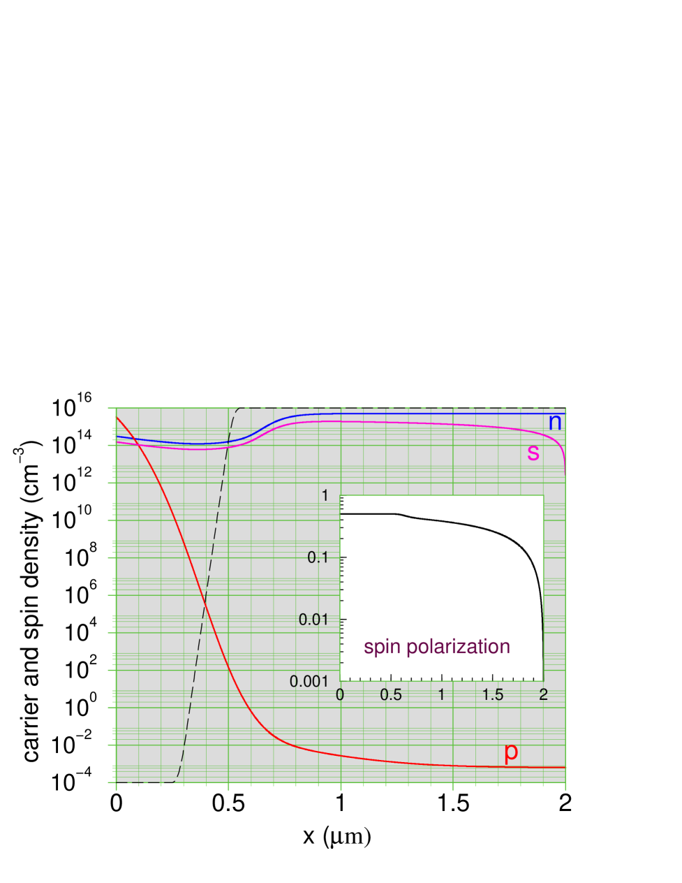
We first discuss the case of (the applied reverse bias from an external battery cancels the forward voltage due to photoexcitation), which is in Fig. 1. Electronic density starts off with the value of at , decreases somewhat in the depletion layer, then rises by more than a decade to reach its equilibrium value of in the region. The hole density sharply decreases from approximately through the depletion layer until it becomes , the equilibrium value on the side. Spin density is at the illuminated surface, and essentially follows the spatial dependence of through the depletion layer, but once in the region it decays towards zero[16]. The surprising feature is the increase of through the depletion layer. In effect, the magnetization of the sample increases by more than an order of magnitude as a result of spin injection. The polarization (Fig. 1, inset) starts at 0.5 at the illuminated surface, stays almost constant through the transition region, then decreases to zero at the right boundary[16]. We checked that these results are robust against changes in and by up to two decades, as long as (so that appreciable spin polarization can be induced in the region in the first place).
Spin polarization clearly survives the depletion layer. This is not an ordinary spin injection in which certain number of spin-polarized electrons tunnel through a contact and the spin density is equal on both sides. What we have, rather, is a spin pumping (leading to spin density amplification) mechanism. Indeed, in optical spin pumping [4] circularly polarized light creates spin polarization of majority carriers (electrons in region) by intensive illumination which generates spins at a faster rate than . Here we illuminate the (not ) region, so we do not have optical spin pumping. The physics is the following: light induces spin polarization of minority carriers (electrons in the region) through optical spin orientation (see Ref. [4]), which diffuse towards the transition region where they are swiftly pushed by the built-in field into their native region. What we have is spin pumping through the minority channel: spin-polarized minority electrons bring spin into the region faster than the spin there relaxes or diffuses away.
In a sense, minority electrons play the role of circularly polarized light. The evidence for that is in Fig. 1. In the region, spin imbalance is present even though the carrier populations are well relaxed in equilibrium. As a result, spin diffusion is controlled by the majority diffusivity constant [4] rather than the minority constant , as would be the case of carrier diffusion. Spin decay beyond the depletion layer is therefore described by the single exponential , where m is the spin diffusion length of electrons in the region. In the -region spin diffusion length is ; electrons diffuse bipolarly with hole diffusivity for a time ns, so that m is of the order of the electron diffusion length in the -region. Since ( in our model), the effective range of spin diffusion is extended far beyond the expected value. The depletion layer acts to extend the range of spin diffusion, with the effect most pronounced for , which is typically the case (especially at lower temperatures).
Our model scheme above constitutes a solar cell, as light illuminates the surface within the electron diffusion length from the depletion layer. As the electron diffusion length almost coincides with , electrons arrive at the transition region spin polarized. The built-in electric field then sweeps the electrons in the -region (and holes back into ). Because of the spin amplification in the -region, the resulting electrical current is spin polarized and can be used for spintronic applications (in a combination with ferromagnetic semiconductors or metals). Our spin-polarized solar cell has the usual I-V characteristics, with 1.03 V open-circuit voltage.
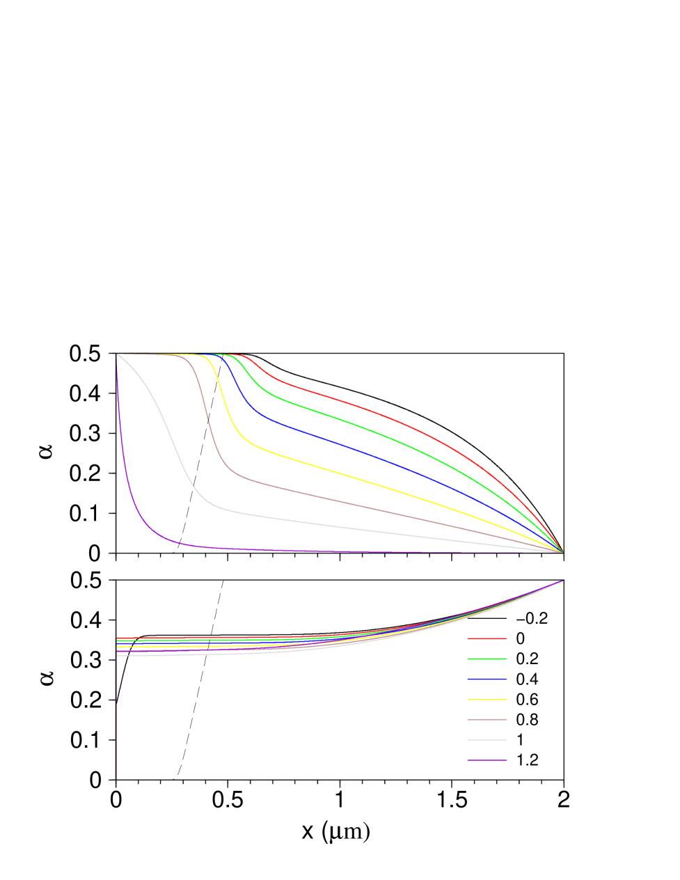
How does spin polarization change with the applied bias ? The calculated profiles for our model device are in Fig. 2 (top). There is a strong monotonic decrease of with increasing . To quantify this dependence we consider the change of the total spin accumulated in the cell (integral of the spin density from to 2); the spin accumulates almost exclusively in the region (where electron density is large). The result is in Fig. 3. Total spin changes by almost 20 times when increasing from -0.2 V to 1.2 V. By (loose) analogy with junction capacitance, we call this effect spin capacitance. The spin accumulation in the region essentially follows the nonequilibrium density of electrons (charges) there, but in the region, where spin diffusion length is much greater than carrier diffusion length, nonequilibrium spin accumulates to a much greater distance; spin capacitance is not trivially connected with nonequilibrium charges. Clearly, after switching off the light the spin is lost, so to “store” spins in the solar cell one needs to supply energy (the fact that will lead to special transient effects related to spin recovery). The reason why depends so strongly on is that changes the extent of the depletion layer: as increases, the width of the depletion layer decreases[13]. Since we are illuminating the same point in all cases, the amount of spin polarization that reaches the depletion layer decreases as the width of the layer decreases (so that the distance from the surface to the center of the layer increases). At large forward voltages (say, V, in Fig. 2), the injected spin essentially decays within , which is shorter than the distance from the illumination surface to the depletion layer. Another effect affecting the dependence of on is the value of the built-in field, which also decreases with increasing . This electronic control of spin polarization could be measured by observing luminescence of electrons in the region (by, say, forcing them to recombine with holes in heterostructures attached to the right surface). The above effects are not limited to optical spin injection. The only requirement is that there is an electronic spin and carrier imbalance (which can be also created electronically) in the p region.
Finally, consider the case of spin polarization injected in the majority (here ) region (say, by ferromagnetic electrodes). There is no light illuminating the sample, and all the parameters and boundary conditions remain as above, except that at all the charge densities are the equilibrium ones, and (a quite favorable case). The calculated for different are in Fig. 2 (bottom). The polarization, as before, is injected through the depletion layer (into minority electrons), but now does not affect that much. Consider what would happen if an region was now attached to the sample from the left, that is, we have an n-p-n transistor. The spin-polarization in the base () would be injected and amplified in the -collector (by the spin-pumping from the minority channel we introduced above). We conclude that spin polarization can be injected all the way through a transistor, from emitter into collector.
We thank Paul Crowell for useful discussions. This work was supported by DARPA and the U.S. O.N.R.
REFERENCES
- [1] G. A. Prinz, Science 282, 1660 (1998); D. D. Awschalom and J. M. Kikkawa, Physics Today 52, 33 (1999); S. A. Wolf, J. Supercond. 13 195 (2000).
- [2] R. Fiederling, M. Kleim, G. Reuscher, W. Ossau, G. Schmidt, A. Waag, and L. W. Molenkamp, Nature 402, 787 (1999); Y. Ohno, D. K. Young, B. Beschoten, F. Matsukura, H. Ohno, and D. D. Awschalom, Nature 402, 790 (1999); B. T. Jonker Y. D. Park, B. R. Bennett, H. D. Cheong, G. Kioseoglou, and A. Petrou, Phys. Rev. B 62, 8180 (2000).
- [3] M. Oestreich, J. Hübner, D. Hägele, P. J. Klar, W. Heimbrodt, W. W. Rühle, D. E. Ashenford, and B. Lunn, Appl. Phys. Lett. 74, 1251 (1999).
- [4] Optical Orientation, edited by F. Meier and B. P. Zakharchenya (North-Holland, New York 1984).
- [5] K. Zerrouati, F. Fabre, G. Bacquet, J. Bandet, J. Frandon, G. Lampel, and D. Paget, Phys. Rev. B 37, 1334 (1988).
- [6] J. M. Kikkawa and D. D. Awschalom, Phys. Rev. Lett. 80, 4313 (1998); J. M. Kikkawa and D. D. Awschalom, Nature 397, 139 (1999).
- [7] D. Hägele, M. Oestreich, W. W. Rühle, N. Nestle, and K. Eberl, Appl. Phys. Lett. 73, 1580 (1998).
- [8] Y. Ohno, L. Arata, F. Matsukura, S. Wang, and H. Ohno, Appl. Surf. Science 159, 308 (2000).
- [9] H. Ohno, Science 281, 951 (1998).
- [10] H. Ohno, D. Chiba, F. Matsukura, T. Omiya, E. Abe, T. Dietl, Y. Ohno, and K. Ohtani, Nature 408, 944 (2000).
- [11] S. Das Sarma, J. Fabian, X. D. Hu, and I. Žutić, Superlattice Microst. 27, 289 (2000); 58th Device Research Conference, p. 95 (IEEE; Piscataway 2000) and LANL Preprint cond-mat/0006369.
- [12] M. E. Flatte and G. Vignale, Appl. Phys. Lett. 78, 1273 (2001).
- [13] N. W. Ashcroft and N. D. Mermin, Solid State Physics (Saunders, New York, 1976).
- [14] A. L. Fahrenbruch and R. H. Bube, Fundamentals of Solar Cells (Academic, 1983).
- [15] J. Fabian and S. Das Sarma, J. Vac. Sc. Technol. B 17, 1708 (1999).
- [16] The spin decay beyond 1.5 m is not a bulk effect. It is caused by our boundary condition which is quite severe (it may physically correspond to a fast spin relaxation at that boundary caused by magnetic impurities), although it does not affect the important region around the depletion layer.