Electronic states and optical properties of GaAs/AlAs and GaAs/vacuum superlattices by the linear combination of bulk bands method
Abstract
The linear combination of bulk bands method recently introduced by Wang, Franceschetti and Zunger [Phys. Rev. Lett. 78, 2819 (1997)] is applied to a calculation of energy bands and optical constants of (GaAs)n/(AlAs)n and (GaAs)n/(vacuum)n (001) superlattices with ranging from 4 to 20. Empirical pseudopotentials are used for the calculation of the bulk energy bands. Quantum-confined induced shifts of critical point energies are calculated and are found to be larger for the GaAs/vacuum system. The peak in the absorption spectra has a blue shift and splits into two peaks for decreasing superlattice period; the transition instead is found to be split for large-period GaAs/AlAs superlattices. The band contribution to linear birefringence of GaAs/AlAs superlattices is calculated and compared with recent experimental results of Sirenko et al. [Phys. Rev. B 60, 8253 (1999)]. The frequency-dependent part reproduces the observed increase with decreasing superlattice period, while the calculated zero-frequency birefringence does not account for the experimental results and points to the importance of local-field effects.
pacs:
PACS numbers: 73.20.Dx, 78.66.Fd, 71.15.Hx, 78.20.BhI introduction
Quantum confinement in semiconductor heterostructures modifies the energy and dimensionality of electronic levels and leads to blue shifts of the optical gaps. Most experimental investigations have focused on the energy region of the fundamental gap, which is easily accessible by photoluminescence and photoluminescence excitation spectroscopies and yields a variety of interesting physical phenomena related to bound excitonic states; relatively few studies of confinement effects on high-energy transitions have been presented. Concerning theory, confined electronic levels close to band edges and the resulting optical properties can be calculated rather simply and accurately by the envelope-function method. The theoretical problem of determining optical spectra of semiconductor heterostructures in the whole visible region is much more complex and beyond the reach of effective-mass methods, as it requires a description of the effects of confinement on electronic states in the whole Brillouin zone.
Interband absorption spectra of tetrahedral semiconductors are dominated by two prominent features, denoted and .[1, 2] The peak (and its spin-orbit counterpart ) originates from band-to-band transitions along the direction, where valence and conduction bands are nearly parallel: this results in a -type critical point, i.e., a saddle point in the joint density of states, which also gives a strong excitonic character to the transition. The peak, instead, has contributions from different parts of the Brillouin zone, but mainly from a region centered around the special point (in units of , where is the lattice constant). The peak has essentially no excitonic character. Blue shifts and splittings of the and transitions were measured in GaAs/AlAs superlattices [3, 4]. More recently, a quantum confinement induced shift of and was measured in Ge nanoparticles embedded in a glassy matrix [5, 6].
A main purpose of this work is to calculate the behavior of and transitions upon confinement in GaAs/AlAs superlattices and in free-standing GaAs layers, which are simulated by GaAs/vacuum superlattices. Besides the obvious interest of the GaAs/AlAs system, the motivation for choosing GaAs/vacuum superlattices is to study confinement effects on and in a system where the electronic states are truly confined in the GaAs layers even at high energies. In GaAs/AlAs superlattices, on the other hand, the band structures of the two constituents far away from the fundamental band edges are rather similar and strong banding effects occur in short-period structures, i.e., the electronic states become delocalized along the superlattice. A comparison between the two systems should therefore elucidate the respective roles of quantum confinement and superlattice band formation in determining the optical properties. Free-standing GaAs films can be produced by chemical etching [7]; GaAs/vacuum superlattices can also be a model for multilayers formed by GaAs and a wide-gap oxide, like Al2O3 or oxidized AlAs (AlOx).
The electronic structure of short-period (GaAs)n/ (AlAs)n superlattices can be calculated from first principles by density-functional theory and norm-conserving pseudopotentials [8]. The computing time grows rapidly with the number of monolayers.[9] Moreover, density-functional calculations of the optical properties suffer from the gap problem [10] and require the inclusion of quasiparticle corrections [11] and excitonic effects,[12] thus increasing the computational cost. Recently a new pseudopotential approach has been developed [13], in which the electronic states of a heterostructure are represented as linear combinations of bulk bands (LCBB). This method can be applied to heterostructures with a large number of atoms per primitive cell with a reasonably low computational effort; it is particularly suited to study how the optical spectra of the bulk are modified upon confinement, since the electronic states of the bulk are the starting point of the technique. The LCBB method is adopted in this work. The results presented here can be the starting point for tackling more complex problems (e.g. the inclusion of local-field and excitonic effects, or the study of confinement in large quantum dots) as well as for comparison with ab-initio calculations when they will become available.
While GaAs and AlAs are cubic materials and have an isotropic dielectric constant, (001)-grown superlattices are intrinsically uniaxial and the component of the dielectric tensor parallel to the growth direction differs from the perpendicular component . The linear birefringence has been measured in GaAs/AlAs superlattices [15, 16]: is of the order of a few percent and has a nontrivial dependence on the superlattice period. Birefringence is much larger in GaAs/AlOx multilayers, where it has been employed to achieve phase matching for second-harmonic generation [17]. A goal of the present work is to calculate linear birefringence [18] and its dependence on energy and superlattice period. The calculations presented here yield only the contribution to birefringence arising from quantum-confinement-induced modifications of the electronic states; they do not account for the intrinsic dielectric anisotropy of a multilayer arising from different boundary conditions for an electric field parallel or perpendicular to the layers [19, 20]. This second contribution to birefringence is in fact equivalent to the inclusion of local-field effects in the dielectric response [21, 22, 23, 24] and is left for future work.
The rest of this paper is organized as follows. In Sec. II we briefly describe a few aspects of the adopted method: the LCBB technique combined with empirical pseudopotentials,[13, 14] as well as space symmetry and the tetragonal Brillouin zone of the superlattice. In Sec. III we present the results for GaAs/AlAs and GaAs/vacuum superlattices. These are divided into three parts: electronic levels (with the added complication of surface states in the GaAs/vacuum system), optical properties via the real and imaginary parts of the dielectric function, and birefringence. Section IV contains a discussion of the present findings also in view of extensions of this work.
II method of calculation
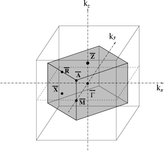
We consider (GaAs)(AlAs)n and (GaAs)(vacuum)n superlattices grown along a (001) crystallographic surface and with period with ranging form 4 to 20. The ideal structure for a lattice-matched system with abrupt interfaces is a simple tetragonal Bravais lattice, with a supercell defined by the basis vectors , , , where is the bulk lattice constant. The reciprocal lattice is also simple tetragonal, with basis vectors , and . The first Brillouin zone is shown in Fig. 1. Superlattice high symmetry points are distinguished from their bulk counterparts by putting a bar over the symbol. An additional symmetry point is defined as follows: if is even, if is odd. The most important zinc-blende points are folded onto superlattice points as follows:
| (1) | |||
| (2) | |||
| (3) |
In the case of a common anion structure like (GaAs)(AlAs)n the point group is , otherwise it is : the latter is the case of (GaAs)(vacuum)n superlattices.[25]
In order to study large scale systems, we adopt a LCBB method [13, 14]: superlattice electronic wave functions are expressed as linear combinations over band indices and wave vectors of full-zone Bloch eigenstates of the constituent bulk materials. Because of the requirement of periodicity, the superlattice potential mixes only bulk states labelled by vectors which differ by a superlattice reciprocal lattice vector : the number of coupled states is hence always equal to , because exactly are contained in the fcc Brillouin zone. The maximum dimension of the basis set is then given by multiplied by the number of selected bulk bands indices. In the case of a GaAs/vacuum superlattice we decide to include the 4 valence bands and the 4 lowest conduction bands in the basis set. In the case of a GaAs/AlAs superlattice the roughest selection is to take both GaAs and AlAs bulk states at each mixed and , orthonormalizing at the end the basis set obtained. But, as GaAs and AlAs band structures are very similar except for the lowest conduction band (see Fig. 2 and details of calculation below), we have verified that it is enough to include only GaAs states for from 1 to 8 together with the 5th band of AlAs (i.e., the lowest conduction band). The resulting set must be orthonormalized. It can easily be seen that the final dimension of the basis is always small ( for the largest supercell). A convergence test is presented at the beginning of Sec. III.
Unlike tight-binding or standard plane wave expansions, the LCBB method allows the intuitive pre-selection of physically important states to be included in the basis set. By contrast with the approach, off- states are directly considered, permitting a correct treatment of - coupling and of all confinement-induced couplings within the Brillouin zone, without the need for a large basis of bulk states. The formalism applied here is strain-free, believing that the small lattice mismatch () justifies a description of the geometrical structure as unrelaxed, with a lattice constant of 5.655 Å averaged over the constituent materials. All trends in the superlattice states obtained by LCBB method were shown to be reproduced [13], with a surprising accuracy (10-20 meV) and a small computational effort, down to the monolayer superlattice and up to large periods.
A local empirical pseudopotential approach is chosen to perform the band structure calculations, both for the heterostructures and the constituent compounds. Since the adopted pseudopotentials are designed for a kinetic-energy cutoff of 5 Ry, [26] bulk eigenfunctions are expanded on a basis set made of about 60 plane-waves at each point. In Fig. 2 we show the band structures of GaAs and AlAs calculated with these pseudopotentials.
The potential term in the one-particle Hamiltonian is built as a superposition of screened, spherical atomic pseudopotentials :
| (4) |
where is a fcc direct lattice (DL) vector and the displacement of the atom of type in the bulk primitive cell. The weight function selects the atom basis which lies on each lattice site, describing the geometrical details and the symmetry of the structure: in the vacuum layers its value is zero. The Hamiltonian matrix elements on the bulk basis set depend on the Fourier transform of the pseudopotentials ; details on the LCBB method can be found in Refs. [13, 14]. We use the continuous-space functions proposed by Mäder and Zunger [26]. In Ref. [26] the empirical parameters are adjusted in order to fit both the measured electronic properties of bulk GaAs and AlAs and some local density approximation (LDA) results for superlattices. It has been verified that the wave functions of bulk and superlattices systems calculated with these pseudopotentials are close to those obtained in rigorous first principles LDA calculations [26]. The As potential depends on the type of nearest neighbors (Ga or Al), thereby describing the local-environment dependence of the atomic potential, by considering the local electronic charge. These pseudopotentials are adjusted to reproduce the experimental GaAs/AlAs valence-band offset (0.50 eV). Bulk and superlattice energy levels are provided in the same absolute energy scale, thus superlattice and bulk eigenvalues can be compared directly. The inclusion of non-local terms is needed to achieve a better description of high energy states, nevertheless we have verified that almost only transitions to the levels originated by the two lowest conduction bands are responsible for the structures in the optical spectra below 6 eV, therefore non-local terms can be neglected for our purposes. At this stage we have also decided to neglect spin-orbit interaction, even if in Ref. [26] it is suggested how to include it. To preserve a correct description of interfaces in GaAs/AlAs superlattices, an As atom bound to two Al and two Ga atoms has been attributed a symmetrized pseudopotential which is the average of the As pseudopotential functions in GaAs and AlAs environments. In GaAs/vacuum superlattices, the dangling bonds at the interfaces are responsible for the appearance of surface states, lying in the forbidden energy gap. The sizeable metallic contribution to low energy transitions is an artifact of the calculation (in a real system dangling bonds would be saturated by the microscopic nature of the interface) and must be minimized by excluding surface states from initial and final states in optical transitions.
Starting from the one-electron band structure, the complex dielectric function is evaluated in a straightforward way by means of semiclassical theory of interband transitions.[2, 27] Tetragonal Brillouin zone integrations are performed using Fourier quadrature with 1056 Chadi and Cohen special points in the irreducible wedge.[28, 29] An empirical gaussian broadening of 0.1 eV has been introduced to obtain smoothed curves. Bulk spectra have been preliminarly calculated integrating over both a fcc Brillouin zone and the corresponding folded tetragonal Brillouin zone, verifying the exact equivalence of the two results.
In Fig. 3 we show the calculated real and imaginary parts of dielectric functions for bulk GaAs and AlAs crystals. Agreement with the experimental positions of the peaks[1, 2] is within a few tenths of an eV: we underline that the empirical approach is free of the band gap problem. The height of the peaks, especially , cannot be correctly estimated without the inclusion of the excitonic contributions and the local field effects.
III results
A Electronic levels
After calculating the single-particle eigenstates of both bulk systems in the whole Brillouin zone, in order to extract the bulk states basis on which to construct the superlattice Hamiltonian, we applied the method described in section II to obtain the single-particle band structures of (001) (GaAs)n/(AlAs)n and (GaAs)n/(vacuum)n superlattices. The period has been varied from to .
When a sufficiently large number of bulk states is used as a basis set for the LCBB method, the results must converge to those obtained with a direct diagonalization of the Hamiltonian for the corresponding number of plane waves. A comparison of LCBB results with the conventional supercell approach was presented in Ref. [13]. Here we perform a convergence test, which consists in calculating the energy levels with four different bulk basis sets of increasing size. Selected results are shown in Tab. I for (GaAs)10/(AlAs)10 and (GaAs)6/(AlAs)6 superlattices. As far as valence states are concerned, dependence of the energy levels on the basis set is below 10-3 eV; for the lowest conduction band levels the dependence on the basis set is generally below 0.05 eV, and falls below 10-2 eV when the 5th band of AlAs is included in the basis. The results of Tab.I justify the use of basis 3), namely to 8 for GaAs and for AlAs, as stated in Sec. II.
In Figs. 4 and 5 we show the superlattice energy bands for : the electron energy levels are plotted along the highest symmetry lines in the tetragonal Brillouin zone (see Fig. 1). Since points in the fcc Brillouin zone are always folded onto the same point in the smaller tetragonal Brillouin zone, the number of occupied superlattice bands is times the number of bulk bands for GaAs/AlAs, times the number of bulk bands for GaAs/vacuum superlattices. The dispersion along the direction is similar to the dispersion along the direction in the bulk, while the other two directions and have no counterpart in the band structures of Fig. 2. In GaAs/AlAs, the dispersion along the growth direction - is much smaller than in the other directions, as expected for superlattice minibands; in GaAs/vacuum the bands along - are flat as tunneling through the vacuum has a negligible effect.
The main differences in the superlattice band structures compared to the bulk can be interpreted in terms of zone folding and quantum confinement effects; it is also interesting to compare the band structures of the two superlattices. Superlattice gaps are larger than bulk gaps: in particular GaAs/vacuum gaps are larger than GaAs/AlAs ones, as a result of a stronger confinement; moreover superlattice band gap widths increase as the superlattice period decreases. The lowering in the crystal symmetry is responsible for the removal of level degeneracies: as an example in the GaAs/AlAs superlattice the threefold degenerate valence states at (spin-orbit is neglected) are split in a twofold-degenerate and a non-degenerate state, while in the GaAs/vacuum superlattices the degeneracy is completely removed.
In GaAs/vacuum bands we clearly see the appearance of states lying in the forbidden energy gaps. The lowest one lies in the gap from -10 to -6 eV, while two other ones lie in the optical gap from 0 to about 2 eV. A fourth state can be recognized at -5 eV around the point, while in other regions of the Brillouin zone it resonates with the energy bands. Indeed, four surface states or resonances are expected from the presence of two dangling bonds at the two interfaces of each GaAs layers. We can identify the surface states by studying the behavior of the probability to find an electron along the growth direction , averaged over the in-plane coordinates. Taking as an example the conduction miniband states at , where the potential profile is characterized by 0.5 eV deep wells in GaAs layers, we observe (see Fig 6) that an electron in a surface state ( in the exemplified case) has a high probability to be localized on the surface and a decaying probability to enter the GaAs layer; on the other hand an electron in a bulk state ( in the figure) has an oscillating probability to be found in the GaAs layers. Both states are obviously evanescent in vacuum. From the position of the uppermost occupied band () it follows that GaAs/vacuum superlattices have a metallic behavior: this is an artifact of the calculations, as our aim is to simulate insulating multilayers made of GaAs and a wide-gap oxide. We get rid of the problem by excluding surface states as initial or final states in interband transitions. This simulates the formation of interface states or defects in a GaAs/oxide superlattice, which would saturate the dangling bonds. The surface resonance cannot be easily eliminated, but it produces small effects on the spectra, since it lies deep in the valence band.
B Optical spectra
The calculated imaginary part of the dielectric function for both GaAs/AlAs and GaAs/vacuum systems are shown in Fig. 7 for different superlattice periods . Here we average over the three orthogonal polarization directions to obtain a scalar dielectric function. The electronic bands of GaAs and AlAs are similar and therefore the two optical spectra present the same features, namely and peaks (see Fig. 3). Superlattice spectra show also these structures, which can be compared directly to bulk spectra: in fact, even if in a superlattice selection rules allow more transitions as a consequence of zone-folding, the tetragonal Brillouin zone is smaller and, at last, all transitions which contribute to superlattice peaks have their equivalent counterparts in the bulk Brillouin zone. As a general remark, the transition is found to blue shift and to split into two peaks for decreasing superlattice period; the confinement-induced shift is larger for the GaAs/vacuum system. On the other hand the transition is split for large-period GaAs/AlAs superlattices, where the electronic states are confined in the two bulk layers leading to a superposition of the two bulk spectra; the two peaks merge into a single one for small period. A single peak with a small blue shift is found for GaAs/vacuum superlattices.
In Fig. 8 the peak energies are plotted as a function of the superlattice period . First we comment on the behavior of : in zinc-blende crystals it comes from transitions along the line, in a region where bulk bands are almost parallel. When the system is confined in the [001] direction, it is not intuitive to describe the consequences of folding of directions. The calculated spectra show that along the folded line transitions subdivide in two main groups and lead to a splitting of the peak in the absorption curves. The two peaks have different oscillator strengths and, except for an intermediate period length, the lowest energy one becomes much stronger and covers the other one. Both peaks undergo confinement effects and are moved towards higher energies in comparison with their bulk position: confinement and the consequent shifts are stronger at smaller well widths. A splitting of the transition with a blue shift of both peaks was indeed observed in GaAs/AlAs superlattices [3]. In the present calculation this is attributed to a splitting of the bulk valence band at the point and along the line, as indicated by the band energies. The results of Figs. 7 and 8 show also that peak displacements are more relevant in GaAs/vacuum superlattices, where quantum confinement effects are stronger due to the vacuum barrier.
The behavior of the peak is substantially different: its main contribution comes from transitions in a region close to the special point .[30] At this point the alignment of both valence and conduction GaAs and AlAs bands is almost flat and the electronic wave functions are completely delocalized all over the heterostructure. This explains why peak in GaAs/AlAs superlattices is at an intermediate energy between bulk GaAs and AlAs peak positions and does not shift when the superlattice period decreases. Our calculated peak positions are in good agreement with experimental data,[31, 3, 4] in particular a splitting of is reported in Ref. [4]. In GaAs/vacuum superlattices the situation changes: electrons near the special point are confined in GaAs layers and the superlattice peak has a weak blue shift at small superlattice periods , going back to the bulk GaAs energy when grows. A single peak obviously arises in this case since there is no AlAs contribution.
At last, we present in Fig. 9 some curves for the real part of dielectric function for GaAs/AlAs heterostructures. We observe that the average, or Penn gap (defined as the energy at which goes through zero) does not depend on the superlattice period. This proves that the center of gravity of valence and conduction bands is preserved, as suggested in Ref. [16]: this follows from compensating effects of a blue shift at the bottom of the band (positive curvature) and a red shift at the top of the band (negative curvature).
C Birefringence and absorption anisotropy
In (GaAs)(AlAs)n (001) superlattices the point group of the zinc-blende structure is replaced by the symmetry group. Cubic crystals present isotropic optical properties, while in a superlattice the reduction in symmetry leads to optical anisotropy in the real part of the dielectric constant (birefringence) and in the imaginary part (absorption anisotropy, or dicroism). The system is uniaxial, with the optical axis directed along the growth direction , thus the dielectric tensor has the form:
| (5) |
where and .[32] The macroscopic dielectric tensor including local-field effects should be found by the procedure of inverting a matrix with off-diagonal elements depending on the reciprocal lattice vectors .[21, 22, 23, 24] In bulk semiconductors the off-diagonal terms have a small effect on optical properties, in superlattices however they are expected to give a sizeable contribution and to depend on the superlattice period.[33] Nevertheless, at this stage we do not include local field effects in our calculation: we directly take into account only the effects of electronic confinement and band folding on optical transitions. Comparison with birefringence data reported in Ref. [16] should allow to determine if one of the two contributions to anisotropy is dominant.
In Fig. 10 we present the frequency dispersion of and , both for real and imaginary parts: the birefringence is dispersionless up to energies close to the direct gap, while at higher energies it presents resonant contributions. We see as expected that folding and confinement can have a greater influence on the resonant part of the birefringence: indeed, transitions from valence subbands couple differently with or polarized electric fields. Note that the interband absorption edge is higher in energy for -polarized light: this is in agreement with well known quantum well and superlattice physics, in which the lowest transition is a heavy hole one and is forbidden for light polarized along .[34] Once again the effect is greater when confinement is stronger (small superlattice period). There is a dispersionless contribution to birefringence at low frequencies of the order of that cannot be distinguished in Fig. 10. As proposed in Ref.[16], we decouple this low energy background birefringence, describing in terms of a fitting function
| (6) |
where is the background contribution we want to isolate, the second term refers to the resonant contribution and is the gap frequency. In Ref. [16] the three parameters , and are extracted by fitting with expression (6) the experimental data. We also fit our calculated curves by means of expression (6). In Fig. 11 we display the fit parameters as a function of the well width: the graphs can be easily compared with the analogous experimental curves presented in Ref. [16]. The gap frequencies we extract by the fit agree both with directly calculated gaps (barely visible in Fig.7) and with the measured ones.[16] shows an increase of the resonance for small periods: the theoretical curve reproduces the trend of the experimental curve, although the calculated values are smaller. The sudden decrease of the measured background birefringence below 40 Å, on the other hand, is completely missing in our results. Moreover the calculated magnitude of this term above 40 Å is remarkably underestimated. The fact suggests that folding effects give only a minor contribution, while the origin of the behavior of must be attributed to local field effects, as already suggested in Ref.[16]. Similar considerations can be made for the GaAs/vacuum system.
The magnitude of the background birefringence related to local field effects can be easily estimated in the case of long wavelength of incident radiation and not too small superlattice periods . If boundaries are assumed abrupt and the constituent materials are supposed to conserve their bulk dielectric functions up to the interfaces, we can apply approximate expressions for and in terms of bulk constituent scalar dielectric functions, and [19]:
| (7) |
| (8) |
where , are the layer thicknesses of the two different materials. Using our calculated values of bulk static dielectric constants in expressions (7) and (8) we find a rough estimate for the local field contribution to birefringence. This value is much larger than the calculated values in Fig. 11, for all superlattice periods , and it is of the same order of magnitude as the the experimental results at intermediate . Only for small periods , when relations (7) and (8) do not hold, the local field correction should become small. Precise calculations of the optical properties including local-field effects are obviously required to clarify this point.
IV Summary and discussion
The energy bands and optical constants of (001)-oriented (GaAs)n/(AlAs)n and (GaAs)n/(vacuum)n superlattices with from 4 to 20 have been calculated by the LCBB method introduced in Ref. [13]. This approach, in which the electronic states of the superlattice are expanded in the basis of bulk states calculated by empirical pseudopotentials, is found to be adequate and practical for superlattices with small to intermediate period; it is particularly useful for calculating how the optical spectra of the bulk materials are modified upon confinement.
Quantum-confined induced shifts of the critical point energies are calculated for both kinds of superlattices and are found to be larger for the GaAs/vacuum system, where coupling between different GaAs layers is only due to quantum-mechanical tunneling and has a negligible effect. For both GaAs/AlAs and GaAs/vacuum superlattices, the peak in the absorption spectrum splits into two peaks with different blue shifts for decreasing superlattice period. This result agrees with the observations of Ref. [3] on GaAs/AlAs superlattices, and is attributed to a symmetry splitting of the valence bands at the point. The blue shifts are again larger for the GaAs/vacuum system. The transition instead is found to be split for large-period GaAs/AlAs superlattices, where the electronic states of the bulk are confined in each layer and the absorption spectrum is the superposition of the two bulk ones; the energy of the peak depends weakly on the superlattice period. The average or Penn gap, defined as the first zero of the real part of the dielectric constant, does not depend on superlattice period, confirming the expectation that a blue shift at the lower absorption edges is compensated by red shifts in the upper parts of the absorption spectrum. The band contribution to linear birefringence of GaAs/AlAs superlattices is calculated and compared with recent experimental results of Ref. [16]. The zero-frequency birefringence is found to be much smaller than the experimental results: the observed static birefringence is attributed to local-field effects as already suggested.[16] The frequency-dependent part of the birefringence arising from band folding and quantum confinement increases with decreasing superlattice period as found in the experiment, although the calculated values are smaller.
The present work can be extended in several directions. Within the LCBB scheme relying on empirical pseudopotentials, a more precise calculation of the optical properties requires the inclusion of spin-orbit interaction and of local-field effects: the latter are particularly important to account for birefringence of the superlattice. A complete description of the peak requires the inclusion of excitonic effects, which account for half of the oscillator strength of the transition in the bulk. For superlattices with very short period, the expansion over bulk states becomes unreliable (unless using a very large basis) and an ab-initio approach is required: it would be interesting to compare the results of ab-initio and LCBB calculations for superlattices with a period from 4 to 8, say, where ab-initio methods are feasible and the LCBB approach is still meaningful.
Acknowledgements
The authors are grateful to M. Cardona, R. Del Sole, A. Stella and P. Tognini for several helpful suggestions and comments and to L. Reining and N. Vast for a critical reading of the manuscript.
REFERENCES
- [1] M.L. Chelikowsky and J.R. Cohen, Electronic Structure and Optical Properties of Semiconductors (Springer, Berlin, Heidelberg 1989).
- [2] P.Y.Yu and M.Cardona, Fundamentals of Semiconductors (Springer & Verlag, Berlin, Heidelberg 1996).
- [3] M. Garriga, M. Cardona, N.E. Christensen, P. Lautenschlager, T. Isu, and K. Ploog, Phys. Rev. B 36, 3254 (1987).
- [4] M. Alouani, S. Gopalan, M. Garriga, and N.E. Christensen, Phys. Rev. Lett. 61, 1643 (1988).
- [5] P. Tognini, L.C. Andreani, M. Geddo, and A. Stella, Phys. Rev. B 53, 6992 (1996).
- [6] C.W. Teng, J.F. Muth, R.M. Kolbas, K.M. Hassan, A.K. Sharma, A. Kvit, and J. Narayan, Appl. Phys. Lett. 76, 43 (2000).
- [7] J.-M. Gérard and B. Gayral, in Confined Photon Systems, edited by H. Benisty, J.-M. Gérard, R. Houdré, J. Rarity and C. Weisbuch (Springer, Berlin, 1999), p. 331; J.-M. Gérard, private communication.
- [8] A. Baldereschi, S. Baroni, and R. Resta, Phys. Rev. Lett. 61, 734 (1988).
- [9] The period of the superlattice is related to the number of monolayers of each material by , where is the distance between neighboring planes of the same atom. For (001)-grown superlattices, as considered here, .
- [10] L.J. Sham and M. Schlüter, Phys. Rev. Lett. 51, 1888 (1983); Phys. Rev. B 32, 3883 (1985); J.P. Perdew and M. Levy, Phys. Rev. Lett. 51, 1884 (1983).
- [11] M. Hybertsen and S.G. Louie, Phys. Rev. Lett. 55, 1418 (1985); Phys. Rev. B 34, 5390 (1986); R.W. Godby, M. Schlüter, and L.J. Sham, Phys. Rev. Lett. 56, 2415 (1986); Phys. Rev. B 35, 4170 (1987).
- [12] S. Albrecht, L. Reining, R. Del Sole and G. Onida, Phys. Rev. Lett. 80, 4510 (1998); M. Rohlfing and S.G. Louie, Phys. Rev. Lett. 81, 2312 (1998).
- [13] L.W. Wang, A. Franceschetti, and A. Zunger, Phys. Rev. Lett. 78, 2819 (1997).
- [14] L.W. Wang and A. Zunger, Phys. Rev. B 59, 15806 (1999).
- [15] A. Fainstein, P. Etchegoin, P.V. Santos, M. Cardona, and K. Tötemeyer, Phys. Rev. B 50, 11850 (1994).
- [16] A.A. Sirenko, P. Etchegoin, A. Fainstein, K. Eberl, and M. Cardona, Phys. Rev. B 60, 8253 (1999).
- [17] A. Fiore, V. Berger, E. Rosencher, P. Bravetti, and J. Nagle, Nature 391, 463 (1988).
- [18] This effect should be distinguished from circular birefringence, or girotropy, which is also allowed by superlattice symmetry but is a -linear effect, i.e., an effect of spatial dispersion. See e.g. Landau-Lifshitz, Electrodynamics of Continuous Media (MIR, Moscow, 1969).
- [19] V.M. Agranovich, and V.E. Kravtsov, Solid State Commun. 55, 85 (1985).
- [20] M. Cardona, in Semiconductor Superlattices and Interfaces, Proceedings of the International School of Physics ”E. Fermi”, Course CXVII, edited by A. Stella and L. Miglio (North-Holland, Amsterdam, 1993), p. 435.
- [21] S.L. Adler, Phys. Rev. 126, 413 (1962).
- [22] N. Wiser, Phys. Rev. 129, 62 (1963).
- [23] W. Hanke, Advances in Physics 27, 287 (1978).
- [24] V.U. Nazarov, Phys. Rev. B 49, 17342 (1994).
- [25] For a description of symmetry properties of superlattices see L.J. Sham and Y.-T. Lu, J. Lumin. 44, 207 (1989).
- [26] K.A. Mäder and A. Zunger, Phys. Rev. B 50, 17393 (1994).
- [27] F. Bassani and G. Pastori Parravicini, Electronic States and Optical Transitions in Solids (Pergamon Press, Oxford, 1975).
- [28] D.J. Chadi and M.L. Cohen, Phys. Rev. B 8, 5747 (1973).
- [29] S. Froyen, Phys. Rev. B 39, 3168 (1989).
- [30] What we call peak may in fact contain weak contributions from the transition, which can be clearly resolved only in derivative spectra. See e.g. Refs. [1, 3].
- [31] E.E. Mendez, L.L. Chang, G. Landgren, R. Ludeke, L. Esaki, and F.H. Pollak, Phys. Rev. Lett. 46, 1230 (1981).
- [32] In GaAs/vacuum superlattices, where the point group is , the system is biaxial with principal axes along [110], [10], [001] and the dielectric constant for in-plane polarization has a slight additional anisotropy. The situation is analogous to heterostructures with no-common atom, where the in-plane anisotropy has been measured: see e.g. O. Krebs and P. Voisin, Phys. Rev. Lett. 77, 1829 (1996); O. Krebs, P. Voisin, D. Rondi, J.L. Gentner, L. Goldstein, and J.C. Harmand, Physica E 2, 59 (1998).
- [33] The macroscopic treatment remains valid as long as the superlattice period remains much smaller than the wavelength of light, otherwise the superlattice should better be viewed as a one-dimensional photonic crystal, where local-field effects embodied in lead to the formation of a band gap for light propagation.
- [34] The polarization selection rule follows immediately from theory, although a precise calculation of absorption spectra close to the fundamental gap should of course include the spin-orbit interaction.


| basis | valence band maximum | conduction band minimum | ||||||||
|---|---|---|---|---|---|---|---|---|---|---|
| n=10 | ||||||||||
| 1) | 0.0000 | -0.0004 | -0.8992 | -2.1127 | -0.8992 | 1.8318 | 1.8303 | 2.0069 | 1.9048 | 2.0063 |
| 2) | 0.0000 | -0.0004 | -0.8990 | -2.1129 | -0.8990 | 1.8173 | 1.8190 | 2.0057 | 1.9014 | 2.0049 |
| 3) | 0.0000 | -0.0004 | -0.8990 | -2.1131 | -0.8990 | 1.7949 | 1.8008 | 1.9911 | 1.8588 | 1.9881 |
| 4) | 0.0000 | -0.0003 | -0.8985 | -2.1130 | -0.8985 | 1.7884 | 1.7957 | 1.9904 | 1.8590 | 1.9874 |
| n=6 | ||||||||||
| 1) | 0.0000 | -0.0118 | -0.8488 | -2.0968 | -0.8489 | 1.9766 | 1.9940 | 2.1730 | 1.9961 | 2.1561 |
| 2) | 0.0000 | -0.0115 | -0.8481 | -2.0970 | -0.8482 | 1.9526 | 1.9567 | 2.1694 | 1.9940 | 2.1535 |
| 3) | 0.0000 | -0.0115 | -0.8481 | -2.0973 | -0.8482 | 1.9062 | 1.9109 | 2.1451 | 1.9618 | 2.1053 |
| 4) | 0.0000 | -0.0113 | -0.8468 | -2.0967 | -0.8468 | 1.9042 | 1.9098 | 2.1440 | 1.9626 | 2.1043 |