The Polarizability and Electric Field-Induced Energy Gaps In Carbon Nanotubes
Abstract
A simple method to calculate the static electric polarization of single-walled carbon nanotube (SWNT) is obtained within the second-order perturbation approximation. The results are in agreement with the previous calculation within the random-phase approximation. We also find that the low energy electronic band structure of SWNT can be affected by an external electric field perpendicular to the axis of the tube. The field-induced energy gap shows strong dependence on the electric field and the size of the tubes, and a metal-insulator transition is predicted for all tubes. Universal scaling is found for the gap as function of the electric field and the radius of SWNTs. The fact that the external field required to induce a gap in SWNTs can be reached under the currently available experimental conditions indicates a possibility of further applying nanotubes to electric signal-controlled nanoscale switching devices.
pacs:
PACS numbers: 71.20.TxThe prospect of nanoscale electronic devices has engaged great interest. Single-walled carbon nanotubes (SWNTs) are significant application as nanoscale devices [1] due to their extraordinarily small diameter and versatile electronic properties [2]. It is suggested that individual SWNT may act as devices such as field-effect transistors (FETs) [3], single-electron-tunneling transistors [4, 5], rectifiers [6, 7], or p-n junctions [8]. The most exciting expectancy lies in the devices fabricated on a single tube [9]. In recent years, the interplay between mechanical deformation and electrical properties of SWNTs have been extensively studied [9, 10, 11, 12]. Tombler et al. [13, 14] used an atomic force microscope tip to manipulate a metallic SWNT, leading to a reversible two-order magnitude change of conductance, and Lammert et al. [15] applied a uniaxial stress to squash SWNTs and detect a similar reversible metal-insulator (M-I) transition. It is also well known that a magnetic field can also change the conductance of carbon nanotubes [16, 17, 18]. A possible electric field-controlled M-I transition are considered to be more exciting because of its easy implementation in the actual applications. Yet, a question remains: Can electric field change the electronic properties of a tube?
In previous studies on electronic transports [19], the potential of a weak longitudinal electric field (bias voltage) in conductors was treated approximately to a slowly change variable in the range of the primitive unit cell. The electric field makes all the electronic energy and the Fermi level have a gradient along the field direction, but the energy-band structure is not change. The controlled potential, such as the gate voltage without a drop of component in the direction perpendicular to the tube axis in the case of FET, is only used to shift the Fermi level or changed the carrier concentration [3]. In the literature, according to our knowledge, there is no report on using a transverse electric field to control the longitudinal electronic transport of conductors. In metallic SWNT, the electrons nearby Fermi energy are nonlocal in the circumference of the tube since their circumference-Fermi wavevector is zero [2], the classic wave-package approximation in slow-change voltage may be not suitable in the presence of the strong transverse electric field. The order electric field is enough to obviously break the rotational symmetry about the tube axis, and create new interband and intraband coupling, which may change the low energy electronic properties of SWNTs, and hence affect the electronic transport. In the other hand, the field is still less than the orders of the atomic interior electric field, can be treated as perturbation.
In this Letter, we first report the result by using a tight-binding (TB) model to calculate the polarizability of SWNTs in the application of an external electric field perpendicular to the tube axis. The calculated polarizability of SWNT is in agreement with the previous results within the random-phase approximation (RPA) [20]. Then we calculate the low energy electronic structure of SWNTs in the electric field. The results show obviously valuable effects: (1) The electric field can always induce an energy gap in metallic SWNTs; (2) There is a maximum gap strongly depended on the radius of the tubes; (3) Universal scaling is found for the gap as a function of the field and the size of the tubes, and the numerical results are testified by the second order perturbation calculations. Our results indicate that the magnitude of the electric field required to induce a sizable energy gap in metallic SWNTs falls into the range of currently available experimental conditions.
In density function theory, single electronic Kohn-Sham Hamiltonian is
| (1) |
where is the effective potential, self-consistently depended on the electronic density , hence the external electric field . is the electrostatic potential of . can be acted as the contribution of the polarized charge, where is the unperturbed electronic density. So we can rewritten (1) as
| (2) |
where is the total perturbed potential. We have
| (3) |
where is the polarized charge density, is the exchange-correlation potential. If or is very small, using the second-order perturbation theory, we know and
| (4) | |||
| (5) |
where is the change of total energy of electrons, can be gained from the unperturbed electronic wave functions and the unperturbed energy levels ,
| (6) |
where , or,
| (7) |
For an approximation, we treat the of (3) as a electrostatic potential. If we suppose the polarization in SWNT is uniform and due to the induced-surface-charge distribution under a constant external field [20], we have , where is the dipole moment per length and R being the radius of tubes. By selecting a set basis, using slater local exchange-correlation approximation, we have numerically solved (3) in small tubes with the calculated TB-electron-energy change . We found the nonhomogenous effect is very small [21]. Here we will only report the results within the uniform polarization approximation. From , we gain the dielectric function ,
| (8) |
Considering the screened electrons are not confined to the surface containing the ions in tubes, after calculating the within RPA, Benedict et al. replaced the of (8) with for calculating . Fitting the result of , they gave for some small radius tubes. If Directly starting from the exactly unperturbed wave functions and energy levels of tubes, we can gain the real distribution of polarized charges. By numerically solving (3), (5) and (7), we found that the exchange-correlation potential maybe decrease partly the depolarized field which is completely attributed to by Benedict et al. However, the order of magnitude of which we need can be identically obtained from one of both (3) and (8).
The nearest-neighbor TB Hamiltonian has been used successfully for calculating the electronic structure of graphite sheet and nanotubes [2]. Our previous works [22] show the model can well describe the electronic perporties and total energy. The Hamiltonian is dependent on the matrix element of potential ,
| (9) |
where is the th ( or ) orbit of the carbon atom, are the Slater-Koster TB parameters in the absence of electric field [22]. Expanding the near the lattice vector ,
| (10) |
where we suppose the is uniform or slowly change in the size of atom. Only considering the nearest-neighbor contribution, we have
| (11) | |||||
| (12) |
where and are the dipole matrix elements, and are overlap integrals which are only slightly affect the electronic energy bands, , and is the position of mass centre of atom and atom. Benedict et al. [20] showed that the can be neglected except the . From the Hamiltonian, we can calculate the total electronic energy in presence of any total electric field . Since the polarizability of electrons is smaller than that of , we only calculate the contribution of . The results are shown at Fig.2. The values of of a few small radius tubes are in agreement with the previous results [20], but is faster increase as the radius increase than the result of Benedict et al. (). Fig.2(b) shows the obtained value of of some tubes using the and , respectively. The is about order of for a few small tubes, slowly increases to about for tube. Since the polarization is nearly constant in SWNT, we will only calculate the effects of a uniform total electric field in this letter. Fig.3 shows the electronic energy bands of a tube. When , where , a sizable gap about is found at , the Fermi wavevector in zero field. As increases, the gap increases, and when , the bands structure is obviously deformed. It is surprising to find that the gap decreases as increases further. When , the zero gap is found, but the Fermi point dramatically moves from .
To probe the above effect in general, we performed the computation for a series of tubes. Fig.4 shows the gap as a function of the applied field in tubes, where is from to . From the figure, we find the determined effect: The electric field can always induce a gap in tubes, and the size of the gap strongly depends on the amplitude of the transverse field and the tube parameter . For any tubes, the gap first increases with increasing field, and reaches a maximum value at the , then drops again. Both the maximum gap and the corresponding are approximately proportional to , and hence inversely proportional to the radius of tubes, i.e.,
| (13) |
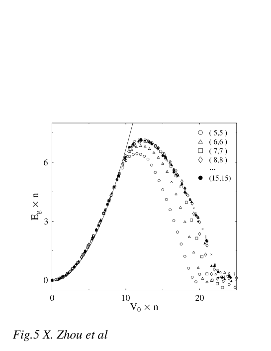
The finding shown in (13) that electric field effects fastly decrease as the size of conductor increases might be the reason why people have not yet recognized the effect in previous studies. The field dependence of the gap is quite similar for tubes with various cross-sectional radii, which invokes us to scale both and up times their original values. The obtained results are shown in Fig.5. From it we do find the scaled gap to be a universal function of the scaled electric field for all tubes. In the low field range, for all calculated eleven tubes there exists a simple relation: , where is a constant, about . In the higher field range, except for a few small-radius tubes such as and tubes, the universal scaling law still holds.
To understand the above scaling relation, we use perturbation theory to calculate the field-induced gap in low field limit. The first-order perturbation approximation only causes shift in the Fermi level, showing no contribution to the gap change. Calculating up to the second order perturbation at point, we obtained the following analytic result
| (14) |
where (= eV) is the hopping parameter in the absence of the electric field [22, 24]. The contribution of the overlap integral , which is very small, is neglected. Obviously, the second-order perturbation calculation gives almost the same scaling relation as the numerical results in the low field, though the obtained (eV)-1 is slightly larger than the numerical result (eV)-1. In the high field range, since the Fermi wavevector is moved from , the perturbation theory becomes not suitable. However, the low field range may be more compatible with the practical application. In order to open a gap in the energy bands of tubes, must be smaller than , and the required electric field is,
| (15) |
where (= ) is the bond length of carbon atoms in the SWNT. Therefore, for example for a tube, the required field is about , and for a tube, it is about . Considering the polarizing, the needed external field is about and , respectively. Our results are encouraged by an important fact that the perturbation approximation is suitable only required the small total field , need not the small external field . Even though is larger, our conclusion is still correct, but needing stronger external field. The magnitude of the required external field for inducing a sizable gap in tubes with larger radius can be reached by the currently available experimental conditions, we wish the above prediction can be checked in near future.
In summary, we have proposed an electric field-induced M-I transition in SWNTs for the first time. The results support the argument that SWNTs can be applied as nanoscale electric signal-controlled switching devices.
The authors would like to thank Prof. H.-W. Peng, Prof. Z.-B. Su and Dr. H.-J. Zhou for many discussions on the results. The numerical calculations were performed partly at ITP-Net and partly at the State Key Lab. of Scientific and Engineering Computing.
REFERENCES
- [1] C. Dekker, Phys. Today 52 (5), 22 (1999).
- [2] N. Hamada, S. Sawada, and A. Oshiyama, Phys. Rev. Lett. 68, 1579 (1992).
- [3] S. J. Tans, A. R. M. Verschueren, and C. Dekker, Nature (London) 393, 49 (1998).
- [4] S. J. Tans et al., Nature (London) 386, 474 (1997).
- [5] M. Bockrath et al., Science 275, 1922 (1997).
- [6] Z. Yao, et al., Nature (London) 402, 273 (1999).
- [7] M. S. Fuhrer et al., Science 288, 494 (2000).
- [8] F. Léonard, and J. Tersoff, Phys. Rev. Lett. 83, 5174 (1999).
- [9] L. Chico et al., Phys. Rev. Lett. 76, 971 (1996).
- [10] A. Bezryadin, et al., Phys. Rev. Lett. 80, 4036 (1998).
- [11] V. Crespi et al., Phys. Rev. Lett. 79, 2093 (1997).
- [12] C. L. Kane and E. J. Mele, Phys. Rev. Lett. 78, 1932 (1997).
- [13] T. W. Tombler et al., Nature (London) 405, 769 (2000).
- [14] L. Liu et al., Phys. Rev. Lett. 84, 4950 (2000).
- [15] P. E. Lammert, P. Zhang, and V. H. Crespi, Phys. Rev. Lett. 84, 2453 (2000).
- [16] H. Ajiki and T. Ando, J. Phys. Soc. Jap. 62, 1255 (1993).
- [17] J. P. Lu, Phys. Rev. Lett. 74, 1123 (1995).
- [18] S. Roche and R. Saito, Phys. Rev. B 59, 5242 (1999).
- [19] , S. Datta, Electronic Transport In Mesoscopic Systems, Combridge Univ. Press, Combridge, 1995.
- [20] L. X. Benedict, S. G. Louie, and M. L. Cohen, Phys. Rev. B 52, 8541 (1995).
- [21] The details will be published in another paper in the future.
- [22] X. Zhou, J.-J. Zhou, and Z.-C. Ou-Yang, Phys. Rev. B 62, 13 692 (2000).
- [23] R. Saito, el al., Phys. Rev. B 46, 1804 (1992).
- [24] C. T. White, D. H. Robertson, and J. W. Mintmire, Phys. Rev. B 47, 5485 (1993); H. Yorikawa and S. Muramatsu, Phys. Rev. B 52, 2723 (1995).