[
Suppression of tunneling into multi-wall carbon nanotubes
Abstract
We have studied tunneling of electrons into multi-wall carbon nanotubes. Nanotube/electrode interfaces with low transparency as well as nanotube/nanotube junctions created with atomic force microscope manipulation have been used. The tunneling conductance goes to zero as the temperature and bias are reduced, and the functional form is consistent with a power law suppression of tunneling as a function of energy. The exponent depends upon sample geometry. The relationship between these results and theories for tunneling into ballistic and disordered metals is discussed.
pacs:
PACS numbers: 73.50.-h, 73.61.Wp, 72.15.Nj]
Tunneling into one-dimensional or quasi-one dimensional conductor is in general a complex process. Not only must the electron tunnel through the classically forbidden region of the tunnel barrier, room must be made in the conductor for the excess charge induced by the tunneling. This process is typically described by coupling the electron to a set of harmonic oscillators with a linear dispersion, resulting in power-law behavior of the conductance as a function of the tunneling energy of the electron. The values of the power law exponent are determined by the tunneling geometry and the properties of the oscillators. Many examples of this phenomenon have been discussed. For example, the 1D electromagnetic modes of microscopic resistors can be modeled in this manner[1], as can the collective excitations (plasmons) of the interacting 1D electron gas[2].
Carbon nanotubes are emerging as an excellent system for the investigation of electronic transport in 1D. Two different classes of nanotubes exist: small diameter (1nm) single-wall nanotubes (SWNTs) and large diameter (10nm) multi-wall nanotubes (MWNTs). Metallic SWNTs are characterized by two 1D channels, and they can have a very long mean free path[3, 4, 5]: . As such, they represent a nearly perfect 1D system. It is well known theoretically that in 1D, transport is strongly affected by electron-electron interactions, producing a system called a Luttinger-liquid[2, 6] (LL) whose low energy states are collective in nature. The tunneling density of states of a LL diminishes as a power law on the energy of the tunneling electron. Experiments[7, 8] on SWNTs have shown that the tunneling conductance vanishes as a power law in temperature and in bias voltage. The value of the exponent has been found to depend on the tunneling geometry, i.e. whether the electron tunnels into the end or the bulk of the tube or between the ends of two tubes, in agreement with theory.
Various experiments on the transport properties of MWNTs have been performed. Experiments with low ohmic contacts attached to MWNTs show interference effects, like Aharonov-Bohm oscillations[9, 10], weak localization[10, 11] and universal conductance fluctuations[10, 11]. These have been used to infer the mean free path, yielding [10]. They also indicate that the current may be predominantly carried in the outer shell of the nanotube. Similarly, transport[10] and scanned probe experiments[5, 12] indicate a typical resistance per unit length of 5-10 kOhm/m.
We present here measurements of the tunneling conductance of MWNTs. In one geometry, metallic contacts to the tube with high resistance are employed. In a second geometry, nanotube/nanotube junctions are created by manipulation with an atomic force microscope. The tunneling conductance of the nanotube/electrode interface is measured as a function of temperature and bias voltage. These measurements show that the tunneling density of states diminishes as power laws and that the exponent depends upon on the geometry.
The MWNTs were synthesized by arc-discharge evaporation and deposited from a dispersion in chloroform onto an oxidized Si wafer. Nanotubes with diameter ranging from 8 to are selected and located using a scanning electron microscope or an AFM. For devices of the first type, gold contacts to the tube are then created using e-beam lithography. This procedure typically leads to contacts with low resistance (), but it also occasionally produces highly resistive contacts (10k). The microscopic origin of the high resistance is not known, but a variety of causes are possible. For example, a thin insulating layer of organic contamination may be on the tube. Here, however, we will merely exploit these accidental tunnel barriers to probe the electronic properties of the MWNT.
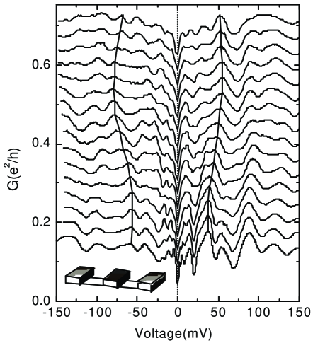
Inset of Fig. 1 shows the schematic of a device consisting of a diameter MWNT contacted to 3 electrodes. The 4.5k resistance measured between the two outer electrodes corresponds to the typical resistance for a MWNT contacted with electrodes that are separated by . This indicates that the contact resistances of the two outer electrodes are low and that the nanotube connecting them is electrically continuous. However, the resistance measured from the inner electrode to either of the outer electrodes is much higher, 140k. The metal/nanotube interface at the inner electrode has thus a low transparency and serves as a tunneling barrier into the nanotube. We therefore use this contact to measure the tunneling density of states of the tube.
Fig. 1 shows a series measurements of the tunneling conductance versus bias for different magnetic fields applied parallel to the tube. The spectra are highly structured. We first note that, at small energies (0-10mV) the spectra display a strongly suppressed conductance. This suppression is independent of . This suppression is the main subject of this paper, but we will first address the complex features at higher energy. The high bias features are quasi-periodic, with an average spacing between the maxima of 25mV. In addition, these features evolve with increasing magnetic field.
The behavior of the high-bias features is consistent with expectations for the effects of subbands on tunneling into a quasi-1D conductor. This typical spacing of the peaks (25 mV) is in reasonable agreement with the theoretical separation expected for van Hove peaks for a 17nm diameter nanotube. The average separation is predicted to be = 29meV, where = m/s is the Fermi velocity. We take as the diameter of the outermost cylinder, because the current has been shown to be carried predominantly by the outermost cylinder. The emergence of (broadened) van Hove peaks in the tunneling density of states demonstrates that the elastic length is at least of the same order as the circumference of the tube. On the other hand, the substantial peak broadening and the lack of accurate periodicity of the peaks indicate the disorder is playing an important role.
The identification[13] of these peaks as broadened van Hove peaks[14] is further supported by their behavior in . The peaks move up and down in parallel field, as expected from the Aharonov-Bohm effect[15]. The magnetic flux through the nanotube gives rise to a phase that shifts the van Hove peaks[16] in energy. This results in a bandstructure that is periodic in magnetic flux with the fundamental period which would correspond to a field of 17.3T. However, the measured spectra in Fig. 1 do not appear to be periodic in field. The reason is not clear yet, but may be attributed to scattering, to the nanotube deformation or to the interaction between adjacent cylinders.
We now turn to the low bias suppression of the conductance. It is independent of , which suggests a different origin than the peaks discussed above. In addition, its dependence on and is very different, as we now discuss.
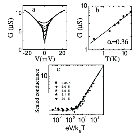
Fig. 2a shows the tunneling conductance of a second sample as a function of at a series of . The MWNT is 12nm in diameter and is attached to 3 contacts; the two outer electrodes are low resistance and the inner one has a resistance of 42k at 300K. Again, this middle electrode is used to measure the tunneling conductance.
A conductance dip centered at zero energy is again observed. As is decreased down to 350mK, the amplitude of the dip increases. In Fig. 2b the zero bias conductance is plotted as a function of in a double logarithmic plot. The straight-line behavior indicates that measured data is well described by a power law behavior with exponent = 0.36. For bias voltages larger than , the voltage dependence of the conductance can also be described by a power law with an exponent, which is again equal to 0.36. This can be seen in Fig. 2c, which shows the symmetrical part of the conductance divided by as a function of the voltage divided by . This figure shows also that the scaled curves for different collapse well into a single universal curve[7]. A similar power-law scaling in and is found in 11 different samples with exponents ranging from 0.24 to 0.37.
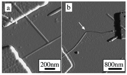
To explore this suppression of the tunneling conductance further, we created devices composed of two MWNTs arranged in different geometries. An AFM tip has been used to move nanotubes[17, 18] using the approach discussed in Ref 18. The end of one tube is pushed against either the end or the middle (bulk) of a second tube. Au contacts are attached to both tubes. Examples of end-bulk and end-end junctions are shown in Fig. 3a and b. The resistance of these junctions varies considerably from device to device, from immeasurably large to 100k. This indicates that the junction between two tubes serves as a tunnel barrier.
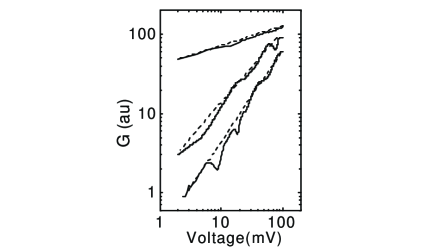
As with the metal/nanotube junctions above, reducing and causes the conductance to decrease significantly, extrapolating to zero at zero temperature. This suppression is significantly more dramatic than in the metal/nanotube junction devices. Fig. 3c shows the as a function of in a double logarithmic scale at = 3K for a bulk-end and an end-end junction. For comparison, the tunneling conductance curve of a nanotube-electrode junction is also plotted. The curve show approximate power law behavior, but with different values for the exponent. We find = 0.9 and 1.24 for bulk-end and end-end junctions, respectively. These exponents are representative of the seven junctions that we have studied.
Overall, our result for tunneling into MWNTs can be summarized in a simple rule. The conductance is given by , where is the excess energy of the tunneling electron, given by the larger of or . To a first approximation, the exponent of the power law is equal to , where the terms represent the properties of the conductor on each side of the junction. We find that 0.3 for the tube bulk, 0.6 for the tube end, and 0 for the Au contact.
We now discuss the possible origins of this low energy suppression of the conductance. The first possbility is the single particle density of states (DOS) of the graphene, the 2D material from which nanotubes are made. The DOS is linearly dependent on energy. Indeed, some samples show a linearly increasing at high (100 mV), that can be attributed to this. At low energies, however, the DOS should be significantly modified. First, the quantization of the energy states due to the transverse confinement should create a series of 1D subbands as discussed above. On energy scales much less than the subband spacing, the DOS should be relatively constant. This is however not observed. In addition, the position in voltage of the minimum in would depend on gate voltage, since the gate voltage shifts the Fermi energy. Again, this is not observed. We therefore conclude that the anomaly is not related to the band structure of graphene.
Another possibility is tunneling anomalies associated with Coulomb interactions that were discussed in the introduction. These lead to power-law dependences: and at zero temperature and zero voltage, respectively. Theoretically, depends on the junction geometry and the properties of the conductor. In one case the conductor is approximated as a classical resistor R[19], and the exponent is then given by: where is the effective resistance seen by the tunneling electron. The second case applies for a ballistic Luttinger liquid. The exponents for tunneling into the end and bulk of the conductor are predicted to be and where depends on the interaction strength in the conductor. Both cases, a resistor and a LL, result in power-law anomalies.
Since these tunneling anomalies are associated with the charge propagation in the conductor, the exponent depends on the junction geometry. If tunneling occurs into the end of a tube, the electron can propagate away from the tunneling site only in one direction. In contrast, for bulk tunneling the net propagation is faster since two different directions are available. This implies that the exponent for bulk tunneling is reduced roughly by a factor 2 when compared to end tunneling. This is seen immediately for the classical resistor case. is divided by two since it is the sum of two resistances in parallel. In case of ballistic resistor in the limit of a small (large interaction strength).
Our measurements qualitatively agree with expectations for tunneling anomalies associated with charge propagation in the conductor. The tunneling conductance displays power law behavior both in temperature and bias voltage. The observed exponents are geometry dependent and obey . However, neither is in quantitative agreement with our measurements, as we now discuss.
We will first focus on the classical series resistor model. In Fig. 2 the resistance between the two outer electrode is =4.7k at 2K. The tunnel barrier is attached to two resitances in parallel. This corresponds to . This value is not in agreement with the experimental value of 0.36. Furthermore, we have studied many other samples with different lengths, and therefore different resistances, but obtain roughly the same exponent. We therefore observe no clear relationship between the exponent and the resistance of the MWNT.
This oversimplified model can be improved if instead of a bare resistor a RC transmission line is taken[20]. C is the capacitance between the tube and the backgate lying 1 micron beneath. However, comparing our measurements with the equations given in ref [21] gives also bad agreement. The voltage dependence of the conductance deviates from a power law and the suppression of the conductance is much narrower in energy.
We now compare our results to the LL model. It has been successively used to interpret tunneling in SWNTs[7, 8, 18], which are well-suited to this model because of the large elastic length and the fact that only two subbands contribute to transport. MWNTs, on the other hand, have shorter elastic length and have a large number of conducting channels[21]. Theoretical calculations[22] have shown that the exponent is reduced by for a wire with channels. The exponent is expected to be further suppressed because the inner cylinders participate in screening, leading to suppression[23] proportional to where is the number of inner metal cylinders.
MWNTs with 10nm diameter have typically 5 inner metal cylinders. Recent experiments on the electrochemical doping of MWNTs[21] demonstrate that the number of occupied subbands is large, on the order of 10. The relative high number of modes together with the inner cylinders is expected to decrease the exponent for MWNTs substantially when comparing with SWNTs. The suppression factor is estimated to be 3. This is not what we observe. Indeed, the exponents 0.3 and 0.6 for bulk and end tunneling in MWNTs are similar to those observed for SWNTs. The exponents for SWNTs are ranging between 0.26 and 0.38 for bulk tunneling, and between 0.5 and 1.1 for end tunneling. Both of these are remarkably close to the MWNT values. Whether this is merely a coincidence or reflects a unified underlying physical origin is not clear.
In conclusion, we have shown that tunneling conductance in MWNTs vanishes at low energies in a manner well-described by a power law in the energy of the tunneling electron. This behavior is most likely caused by suppressed charge propagation of the injected quasi particle away from the tunneling site. However, neither a model of the MWNT as a diffusive conductor nor as a multichannel ballistic conductor gives a satisfactory account for our results. Future work, both experimental and theoretical, is necessary to clarify the nature of the tunneling suppression that we observe.
We acknowledge D. Averin, R. Egger, E. Graugnard, M. Fuhrer, P. Kim, Y. Nazarov and S. Tans for discussions. We thank J.-P. Salvetat, L. Forro, A. Rinzler and R. Smalley for the nanotube materials. This work was supported by DOE, by DARPA and by the Swiss NSF.
∗ present address: TUDelft, 2628CJ Delft, Netherlands.
REFERENCES
- [1] G.-L. Ingold and Yu. V. Nazarov, Single Charge Tunneling, edited by H. Grabert and M. H. Devoret (Plenum, New York, 1992).
- [2] M. P. A. Fisher, L. I. Glazman, Mesoscopic Electron transport, edited by L. Sohn et al. (Kluwer Academic Publishers, 1997); J. Voit, Rep. Prog. Phys. 57, 977 (1995).
- [3] C. T. White and T. N. Todorov, Nature 393, 240 (1998).
- [4] S. J. Tans, et al., Nature 386, 474 (1997); M. Bockrath, et al., Science 275, 1922 (1997).
- [5] A. Bachtold, et al., Phys. Rev. Lett. 84, 6082 (2000).
- [6] R. Egger and A. O. Gogolin, Phys. Rev. Lett. 79, 5082 (1997); C. Kane, L. Balents, and M. P. A. Fisher, Phys. Rev. Lett. 79, 5086 (1997).
- [7] M. Bockrath, et al., Nature 397, 598 (1999).
- [8] Z. Yao, et al., Nature 402, 273 (1999).
- [9] A. Bachtold, et al., Nature 397, 673 (1999).
- [10] C. Schönenberger, et al., Appl. Phys. A 69, 283 (1999).
- [11] L. Langer, et al., Phys. Rev. Lett. 76, 479 (1996).
- [12] H. Dai, E. W. Wong, and C. M. Lieber, Science 272, 523 (1996).
- [13] Measurements on other samples containing a backgate show similar peaks, which are mostly independent on gate voltage. This allows to rule out an origin due to coulomb blockade or to interference.
- [14] J. W. G. Wildöer, et al., Nature 391, 59 (1999); T. W. Odom, et al., Nature 391, 62 (1999).
- [15] H. Ajiki and T. Ando, J. Phys. Soc. Japan 62, 1255 (1993); W. Tian and S. Datta, Phys. Rev. B 49, 5097 (1994).
- [16] This Aharanov-Bohm effect is different than the one observed in ref [9], which is based on interference effect.
- [17] T. Hertel, R. Martel, and P. Avouris. J. Phys. Chem B 102, 910 (1998); L. Roschier, et al., Appl. Phys. Lett. 75, 728 (1999); L. Lefebvre, et al., Appl. Phys. Lett. 75, 3014 (1999).
- [18] H. W. C. Postma, et al., Phys. Rev. B 62, R10653 (2000).
- [19] P. Delsing, et al., Phys. Rev. Lett. 63, 1180 (1989); A. N. Cleland, J. M. Schmidt, and J. Clark, Phys. Rev. Lett. 64, 1565 (1990); M. H. Devoret, et al., Phys. Rev. Lett. 64, 1824 (1990); J. P. Kauppinen and J. P. Pekola, Phys. Rev. Lett. 77, 3889 (1996); W. Zheng, et al., Sol. State Com. 108, 839 (1998).
- [20] Yu. V. Nazarov, Pis’ma Zh. Eksp. Teor. Fiz. 49, 105 (1989) [JETP Lett. 49, 126 (1989)]
- [21] M. Krüger, et al., cond-mat/0009171.
- [22] K. A. Matveev and L. I. Glazman, Phys. Rev. Lett. 70, 990 (1993).
- [23] R. Egger, Phys. Rev. Lett. 83, 5547 (1999).