Electronic Transmission Through Metallic Nanowires:
Generalized Scattering Matrix Approach
Abstract
An easy to implement and powerful method for the solution of 3D scattering
problems that can be well described by Helmholtz equation is presented.
The matrix algebra used provides excellent stability versus
the number of junctions as well as great computational speed.
The matrix truncation method yields an easy single-parameter convergence procedure.
Subsequently, some aspects of the electronic transport through metal nanowires are
studied by the use of Landauer’s scattering approach to the conductance.
We predict the existence of current vortex-rings patterns due to sharp enough
narrow-wide connections in atomic size point contacts.
Longitudinal resonances between scattering centers provide a simple physical picture
for the understanding of negative
differential resistance in ideal monoatomic contacts. Relatively long nanowires with
high geometrical perfection -like those recently observed by Transmission Electron
Microscopy- are modelled exhibiting resonant tunnelling and total
reflection at given incident energy intervals.
pacs:
pacs numbers: 73.23.-b, 73.23.Ad, 73.63.Nm, 73.63.RtFuture daily-life technology will be greatly based on miniaturization of both electronic components and optical devices. State-of-the-art research has already prototyped tools using simultaneously both electrons and photons confinement. For instance, in artificially created electromagnetic micro-cavities interaction light-matter can best be described by new concepts like those of “cavity polaritons”[1], devices in which the light emission process can be extra-ordinarily fast. Also, quantum well lasers utilizing two-dimensional electron gas and optical modulators with quantum confinement effect are now practically used. The ultimate integration of any opto-electronic device has to overcome the theoretical and practical problem of the waveguiding at tiny sizes for both electrons and photons[2]. Consequently, it is not surprising the huge research effort devoted, in the last decade, to these waveguides themselves: metallic wires at the nanometer scale and optical waveguides at the micrometer scale. A common characteristic lays on the basis of these waveguide systems: elastic scattering processes are dominant for transport. Metallic atomic-size wires and micro-optical guides present lateral dimensions of the order of the wavelength associated to the particles passing through. Helmholtz equation governs elastic flux of waves through a general dispersive system (note here that the independent free-electron stationary Schrödinger equation is equivalent). Therefore, the ability to calculate solutions for this equation is of great importance.
As mentioned above, the experimental and theoretical study of metallic nanowires, namely their electrical and structural properties, has been focus of intense research in the last decade (see e.g articles in Ref. [3] as well as the various experimental works of Ref. [4], and the theoretical works in [5]). However, only very recently, the combination of Scanning Tunneling Microscope (STM) with Transmission Electron Microscopy (TEM) has achieved atomic-resolution images of metallic nanowires[6, 7, 8, 9, 10, 11, 12]. In particular, ultrathin gold wires have been observed exhibiting a striking geometrical regularity in some cases. Here we intend to look at some possible effects due to the ideal geometry of these nanowires. Due to the simple -therefore general- phenomenology studied, the same physics is expected to be found by more sophisticated approaches.
The paper is organized as follows: first we present a Generalized Scattering Matrix method for the solution of Helmholtz (or Schrödinger) equation in section I. Though the formalism developed can be applied to general scalar wave propagation problems and even scattering of light in some cases, we use it later to address the problem of conduction through atomic-size contacts: In section II we focus on the study of electronic conduction through metallic nanowires with several models. Finally, in section III we summarize our results.
I Scattering Matrix Method
As a start, let us write the 3D time-independent Schrödinger equation in and (Fermi wavelength and Fermi energy) units:
| (1) |
A general waveguide geometry can be formed by discretization in constant section slices (where the confining potential only depends on ). For a quantum waveguide of constant section, the solution of the time-independent Schrödinger equation is separable as: , being the separated equations:
| (2) |
| (3) |
where the longitudinal wavevector is the arbitrary separation constant. The general solution for the propagating part of the wave function is: , where and are arbitrary constants to be determined. In we have a generic quantum well determined by the confinement potential . We will assume that this well has some “hard wall” boundary conditions at a given limit. The discrete set of eigenvalues (being ) can be found analytically or numerically. The known solutions of equation 3 form a complete basis of transversal eigenfunctions inside the hard-wall limit, so one can write the complete solution for the uniform section waveguide as an expansion in this basis:
| (4) |
where the quantity in between brackets can be seen as the correspondent complex coefficients of the expansion. This leads to a vectorial notation in which the coordinates of in are given by , where the -th elements of vectors and are and . The basis is completely characterized by the confining potential .
A Scattering Matrix of a Single Junction.
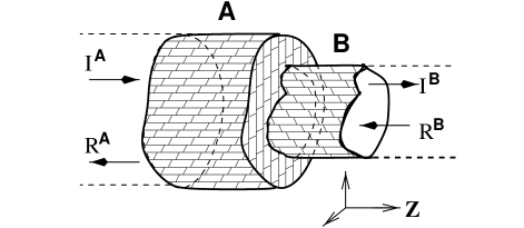
Mode-matching techniques can be used to obtain the scattering matrix (SM) for the simplest non uniform system: a single junction. A single junction discontinuity is shown in Fig. 1, the general solution and derivatives in the two uniform waveguide sections are given, in matrix notation, by:
| (5) |
| (6) |
where diagonal matrix is given by (analogous definition for ).
Continuity condition for the wave function and its normal derivative at the junction leads to these following two matrix equations:
| (7) |
| (8) |
Here, matrix characterizes the intermode scattering or mode coupling due to the step discontinuity and is defined by overlap integrals. The change of basis matrix to change from basis to basis , , can only be defined if the eigenvectors of the basis can be expanded in terms of basis ; this implies that the definition domain for should include the one for i.e., in geometrical terms, the hard-wall closed line of is completely inside the one for (see Fig. 1).
The element of the change of basis matrix is given by:
| (9) |
where is the area in the plane enclosed by the hard-wall limit correspondent to . From matrix equations 7 and 8 the generalized SM defined as:
| (10) |
can be readily obtained and is given by:
| (11) |
| (12) |
| (13) |
| (14) |
where:
| (15) |
| (16) |
| (17) |
| (18) |
The analysis of a single junction similar to that shown in Fig. 1 with the only difference that now includes , is completely analogous, equivalent equations and SMs are given in the next. Following two matrix equations are equivalent to eq. 7 and 8:
| (19) |
| (20) |
The same definition (eq. 9) is valid for the change of basis matrix to change from to . From matrix equations 19 and 20 the scattering matrix, defined as stated in eq. 10, is given by:
| (21) |
| (22) |
| (23) |
| (24) |
where same definitions 15-18 are valid if one swaps and indexes.
B Scattering Matrix of many-junction structures
The SM of a composite waveguide structure may be obtained by combining SMs of the corresponding junctions. The procedure to obtain the SM of a composite waveguide structure is described in the following.
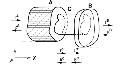
Let us assume two consecutive junctions joined by a uniform waveguide section as shown in Fig. 2. Individual SM for both single junctions have been obtained as described above and are defined by:
| (25) |
| (26) |
We will describe now formulae to obtain the total SM of the system defined by:
| (27) |
Since the middle connection is a uniform waveguide we can write:
| (28) |
where is a diagonal matrix with elements given by: . With some matrix algebra from matrix equations 25 and 26, using 28, one can obtain the wanted SM of the whole composite system:
| (29) |
| (30) |
| (31) |
| (32) |
where the diagonal identity matrix has been noted as “1” and is:
| (33) |
This same solution can be expressed in other equivalent ways, nevertheless, we found that this is the best formula to reduce computational time since it requires minimum number of matrix inversions: just one.
For a greater number of junctions system, one starts similarly calculating each single-junction SM. Then, the iterative use of this combining recipe leads to the total SM.
C Cylindrically symmetric systems
In the case of cylindrical symmetry, overlapping integrals get easier since can be reduced to one dimension. Let us detail the expressions for the simple case of plane hard-wall confinement.
The symmetry assures that will be no matching of modes belonging to different acimutal quantum numbers [13], so we obtain a 2D equivalent problem for each . The number of 2D problems that one needs to solve increases with tubes width.
Let us consider a cylindrical uniform waveguide section. Electrons are confined with hard-walls at distance of axis , the confining potential is only function of the distance to this axis. Thus, eq. 1 can be separated in cylindrical coordinates, so that the wavefunction can be written as:
| (34) |
where:
| (35) |
being and to be specified below.
Due to the cylindrical symmetry, the problem can be considered separately for each value of ; therefore, in the following, we will focus in the problem for a fixed .
Functions are the solutions of the separated radial equation:
| (36) |
Let us consider the basis of these radial eigenfunctions defined between and : . Then, the wavefunction can be expressed as an expansion in the basis with some coefficients that depend on and , written as above. In matrix notation this is:
| (37) |
where:
| (38) |
| (39) |
being the component of the wavevector for the subband .
Therefore given the (infinite) set of complex numbers and given the basis , we have completely described the wavefunction . For any other radius the solution is, obviously, analogous.
This formulation of the problem gives the correspondent SM for each quantum number. Matrix equations are the same than in previous sections if we specify the change of basis matrix and the transverse wavevector diagonal matrix . So that for a single junction joining tubes of radius and , being lower than (similar to that represented in Fig. 1) we have:
| (40) |
| (41) |
being given by the transversal quantized levels.
The calculation of the relevant integral, for the simple case of hard-wall boundary conditions ( constant inside the tubes), yields:
| (42) |
In this case, radial wavefunctions are given by:
| (43) |
being the zero number of , the Bessel function of integer order , and the component of the wavevector given by: .
D Conductance Calculations
Within this framework, one can easily evaluate the conductance of a two terminal system on the basis of Landauer’s scattering approach [14, 15], which is given by the formula:
| (44) |
where the sum runs to all propagant modes in the input lead (propagant modes are defined as those with a correspondent real , while the rest -those with imaginary longitudinal wavevector - are called evanescent). Here, is the universal spinless quantum of conductance with the value . The transmission probability for incidence through mode can be easily obtained and is given by:
| (45) |
where is the element of the matrix given in equation 31, the sum runs to all propagant modes of the final lead, and are the and longitudinal wavevectors of the final and initial tubes respectively.
E The truncation method
One crucial point in the correct calculation of the SM of a quantum waveguide junction is the right truncation of two infinite series of modes representing wave functions at both sides of the junction.
In the analysis of junctions, different converged results may be obtained for different ratios of the number of modes retained on each side. This convergence problem is usually referred to as relative convergence phenomenon [16, 17]. Theoretical studies have found that the correct converged result is obtained if the ratio of modes on each side is taken the same as the ratio of the corresponding waveguide widths [17]. Further calculations give another optimum value for this ratio which is 1.5 times the ratio of waveguide widths [18].
In our analysis we have found that one can generalize this optimal ratio criterium to an optimal “procedure” which gives different ratios in different cases. Our approach is based on observations of the coupling between different modes at waveguide junctions.
For simplicity, let us consider the 2D axial symmetric hard-wall problem of a single junction like the one shown in the inset of Fig. 3. Assuming incidence from left to right and for a fixed incident mode , the plot of the coupling integral versus “wide” transversal modes, , is “peaked” at such that its transverse wave vector satisfies . Thick dots in Fig. 3 represent values of this overlaping integral, the peak can be clearly seen at (in this simple case and ). In a “mean field approximation” [19] true overlaps are approximated by a uniform coupling to all modes within one level spacing, represented by the dashed line in Fig. 3. This approximation gives excellent total transmission results when the difference in widths is big [20]. We can conclude that exists a given band of modes of the wide side effectively coupled to the -th mode of the narrow side. One needs to take into account all modes in this continuous interval to assure a correct representation of the “narrow” mode in the “wide” basis of transversal eigenfunctions. The truncation recipe that we have found is based on this observation.
Though we have shown here a simple case, this mode matching scheme holds for different confining potentials and presumably for all of them (in particular we have checked some axial symmetric potentials in 2D and 3D: hard-wall, soft wall and harmonic. Also some non symmetric 2D and 3D potentials have been checked: hard-wall and soft-wall) Consequently, for one single junction similar to that in Fig. 1, the truncation procedure is as follows. Given transversal levels sorted in crescent energy: (i) Take one arbitrary number of modes in the narrow side, greater or equal than the number of propagant ones. This implies that can be written as , where is the number of propagant modes and is the number of evanescent modes in the narrow tube. (ii) Take all modes of the wide side which are effectively connected to the ones chosen in the narrow side. This implies that we should use every wide-mode whose energy lies bellow given by . In other words, is the energy correspondent to the level of the narrow side.
For the truncation in the case of a greater system, in which the number of junctions is larger, the procedure is the same but choosing the narrowest of the whole system (i.e., the one that has the sparser transversal energy levels) as the tube to define the threshold transversal energy . This value is then used to fix the number of modes retained at the rest of the uniform waveguide sections of the system.
Using this procedure, the number of evanescent modes taken in the narrowest tube is the only free parameter, it can be tuned for proper convergence of the results. In Fig. 4 we can see the convergence of the conductance versus (note that the number of evanescent modes taken into account in the wide side could be quite larger than ). The plot has been done for the 3D “hard-wall” problem and is quite representative of the general behaviour for different confining potentials.
The problem converges for equal four with an error of . The crucial point is that this way of making the truncation ensures good coupling of every mode at the narrow side, and the appropriate description of these modes is the main influence in conductance values. It is worth to notice here that matrices involved are rectangular in general. Algebraical operations done assure the appropriate use of them: no numerical inversion of non-squared matrices has been done. One good property of this particular way of treating matrices involved is that flux is conserved with any truncation chosen; this implies that even for (where is the total transmission and is the total reflection for one particular propagant mode in the initial lead).
By the use of the matrix algebra proposed here, numerical unitarity and stability are achieved with ease. The SM formalism used, in which information from both ends of the system is taken in each step, avoids numerical roundoff errors accumulation in particular when combined with a suitable change of transversal basis as a function of the local width of the system. The truncation procedure explained above is the key for the achievement of these characteristics: it produces a self filtering of numerically unstable components without further data manipulation, hence the unitarity (to compare with recursion-transfer-matrix methods see for instance Ref. [21]).
II Metallic Nanowires
For several years now and in various experimental ways, the formation of ultrathin wires between two macroscopic pieces of metal has been routinely achieved and characterized [3]. However, direct information about the atomic structure of these wires has not been available until recently when various experiments have achieved atomic resolution TEM images on gold nanowires [6, 7, 8, 9, 10, 11, 12]. One of the most interesting features seen is the almost ideal perfect geometry, as well as surprising helical structures[22, 10]. To the date, theoretical work has been focused on the study of the stability and electronic structure for the thinnest monoatomic chains [23]; while for the helical wires works have been focused esentially in the prediction of the very structure for various metals [24], and the influence of helicity in the ideal ballistic conductance [25]. In the second part of this work -by making use of the calculation method we have just described above- we approach this problem. We will point out some remarkable effects in the current and conductance patterns due to the ideal sharp geometries observed, these effects are valid in the presence or not of helicity. For a study on the effects of global smooth shapes in the conductance of atomic-scale 3D contacts see Ref. [26].
A Vortex rings in narrow-wide connections.
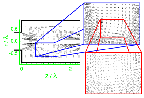
A narrow-wide connection is eventually formed when an unsupported gold nanowire is done by experimental means[7, 8, 10]. This can be modelled by a simple single junction connection in a 3D wire similar to that sketched in Fig. 5. Previous theoretical work on 2D nanowires have pointed out the existence of a vortex structure, for the quantum current density, as a result of a narrow-wide connection. Interestingly, a change of pattern from laminar to “turbulent” flux is obtained for ballistic 2D free-electron calculations [27]. In the analogous simplest case for 3D wires we observe a similar behaviour and transition, the onset of vortex structure formation is intimately linked to the income of the second transversal level in the wider part.
In Fig. 5 and 6 we can see the charge and the current density for this 3D narrow-wide structure. The width of the narrow wire allows just a single propagating channel while the wide part allows two channels, this is the minimum required to exhibit the vortex structure that is remarked in Fig. 6. Periodic charge and current density structures are formed along the final wider tube, this can be readily explained in terms of constructive and destructive interference patterns for the only two channels occupied in the wide lead. There are points with charge density zero regularly distributed at both sides of the charge density maximums in Fig. 5, these points are vortex centers in the quantum current map of Fig. 6. Note that, due to the axial symmetry, these vortex points define rings in real space, and the flux sourrounding them torus surfaces.
When the wide lead gets much wider, many transversal levels come up and the charge density structure gets irregular as can be seen in Fig. 7. The same explanation remains valid this time: the pattern results from the interference of many -in this case- longitudinal wavelenghts, the period of these patterns increases with the number of levels involved, eventually it gets seemingly non periodic as the case seen in Fig. 7 where no regular pattern is observed.
These results could be important for the understanding -and therefore control- of coherent waves by tuning geometrical parameters. In particular the transition from a regular one dimensional lattice of maximums to a disordered pattern by changing the width of the outgoing waveguide could be amenable of experimental verification (may be with electromagnetic waves rather than electrons).
B Resonances inside Wide-Narrow-Wide structures
A single junction, as the one seen in previous section, can be regarded as a scattering center in general terms. Realistic wires have atomic structure and therefore many possible scattering centers for the conduction electrons passing through. The inclusion of increasing number of scattering centers gives rise -as we will see- to a richer phenomenology. In this subsection we will focus in the case of just two scattering centers: a wide-narrow-wide (WNW) junction. Two (strong) scattering centers suffice to predict negative differential resistance in point contact experiments.
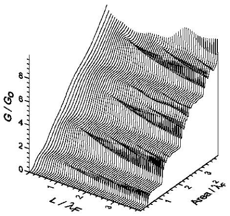
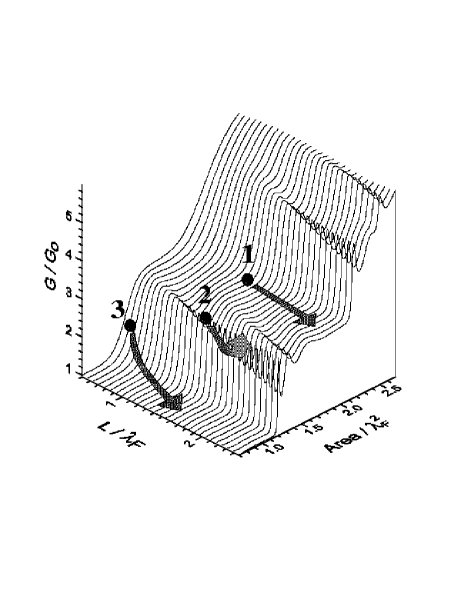
The ballistic conductance of a WNW structure, as the one in the inset of fig. 4, presents a dense resonant behaviour [28] as a function of the narrow area and lenght as can be seen in fig. 8. Being this a very simplistic model, it is a fair representation of what can be expected when we have these main ingredients: a couple of strong scattering centers at a given distance, , and transversal confinement (characterized by the area ). In these cases we can expect a “wavy landscape” for the conductance as a function of (, ), though may be not the same than the one in Fig. 8. Clearly, however, the variation of any of these relevant parameters can eventually give any derivative. This diversity of results is what -we will see- is possible for the case of monoatomic contacts.
Within this very simple WNW representation of atomic size contacts, we can easily locate the zone in Fig. 8 that reasonably belongs to monoatomic (or very few atoms) contacts for typical metals. This zone is what we have represented in Fig. 9, on it we have labeled three different points belonging to 3 different possible particular geometries or ideal contacts. Arrows indicate the evolution due to an eventual stretching process of these few-atoms contacts. Before breaking, seems reasonable to think that the effective lenght will increase and effective area will slightly decrease [28, 29], this is what the arrows indicate. Now, as can be seen, as a function of the starting spot, the subsequent evolution of the conductance can be very different. If we are initially located in point 1, the evolution will be mostly quantized (values very near ) and essentially horizontal; the probability of this event to happen is quite high due to the great number of points in the plane (, ) belonging to this type. However, there is a good chance of falling in a place like the one labeled 3, in this case -as the arrow indicates- we expect to observe a decreasing of before breaking the contact. Finally, there is a little but non negligible chance for our starting point to be like the labeled 2; in this case, since we are located in the minimum of the “valley”, further stretching will make an increase in the conductance as indicated.
The behaviour for case 2 is the more surprising since it predicts increasing of conductance while stretching the wire. Should this model be valid, it could be expected to be found for given geometries and/or metals. In fact there is compelling experimental evidence of negative differential resistance for the case of Aluminum[30, 31], and theoretical explanation in terms of atomistic density functional calculations [32] for the case of relatively wide cross-section wires. Our present free-electron result provides a helpful simple view of good part of the relevant physics in these systems, a complementary piece of the whole picture, especially relevant for the few-atoms-contact case.
C Resonant Tunneling in periodic WNW structures
Long physical wires have their thinnest expression in what we can call monoatomic (in width) long wires. The existence of -relatively long- monoatomic gold wires has been experimentally reported [9, 12, 33] and theoretically studied [23, 22, 34] very recently. In a chain like this, each atom is a system on its own that holds localized electronic states in addition to those extended states responsible for conduction. Very simple modelling of this can be done by the repitition of a WNW structure. As we will see, this periodic repetition gives rise to a long chain of 3D “resonance boxes”. With the selection of proper dimensions for the geometrical parameters of these boxes, localized states can be contained inside. The correspondent energy levels of this states can be an open door for resonant tunneling phenomena in these 3D structures. This is proved here for a sufficiently long periodic wire.
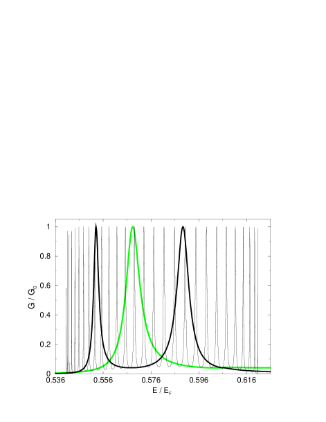
For a clear exhibition of resonant tunneling phenomena in 3D structures let us start with the standard WNW problem as shown in Fig. 10. The evaluation of versus incident energy yields the expected quantized steps with resonance oscilations overimposed. There is a threshold energy at marking the onset of the first propagating level in the narrow tube, which is seen as the first jump in conductance. Now, if we mantain the same geometry but we add -in the central narrow tube- a wider box as shown in the inset, we can clearly appreciate the appearance of a resonant tunneling peak quite before this threshold energy. This is completely analogous to the obtained in 1D and 2D models.
It can be clearly prooved that perfect transparence is achieved at the resonant tunneling energy. Not only the value of transmission gets to 1 at a given E, but the periodic repetition of this structure does not filter down conductivity but simply increases the number of peaks. There is a new peak for each 3D quantum resonant box we add: a splitting effect between degenerate localized levels is proved as can be clearly seen in Fig. 11. In this figure, a zoom of the resonant peak is seen for the cases of 1, 2 and 28 resonant boxes.
Perfect transmission peaks are not the only consequence of interference, total reflection is also obtained as can be seen in Fig. 12. A “band like” structure appears as a consequence of the periodicity imposed in the chain of 28 boxes. There are intervals of energy where transmission is nearly one and intervals where it is practically zero, this is in connection with conduction bands and energy gaps of simple one dimensional band theories [35]. The complete inhibition of transmission is not obtained in pure 1D problems while for 2D and 3D problems total reflection is naturally achieved[36].
III Conclusions
We have developed a formulation of the Scattering Matrix method to solve general three dimensional waveguide problems. The truncation method, based on the way the mode coupling is done, provides quick convergence of results with one single parameter to be tuned: the number of evanescent modes in the narrowmost part of the system. The method has been already successfully used for the calculation in optical waveguides [37] and electronic ballistic contacts[28, 29, 38, 39]. Examples of convergence tests and calculations have been also shown. In particular, we have studied with some detail the problem of quantum conductance in metallic nanowires. Various simple models of crescent number of junctions have been studied. For narrow-wide connections charge density and quantum current patterns have been shown, interestingly vortex rings are obtained for this simple geometry in analogy to previous 2D calculations. This vortex structure starts forming a regular pattern and becomes apparently disordered with increasing tubes width. The calculation for wide-narrow-wide connections gives rise to strong resonant behaviour of the conductance as a function of width and length of the contact. Due to the very recent appearance of experiments in which impressively straight nanowires have been imaged, seems pertinent a closer look at this idealized geometry model. Therefore, interpretation of WNW results, leads to the prediction of several behaviours of the conductance in the last plateaus of an experimental breaking proccess; in particular negative differential resistance can be expected. Further addition of junctions to form periodic WNW structures gives rise to Resonant Tunneling effects in what we can think of as a simple model for a long periodic nanowire. Opossite to 1D models and analogous to 2D, not only perfect transmission is obtained for the resonant tunneling energy but perfect reflection appears for some finite intervals of energy.
IV Acknowledgements
The authors are grateful to M. Nieto-Vesperinas, A. García-Martín, E. Tosatti, J. J. Kohanoff, M. Okamoto, T. Uda, K. Takayanagi and K. Terakura for enlightening discussions. One of the authors (JAT) acknowledges funding support from: European Union through TMR grant ERBFMBICT972563 and Human Capital and Mobility Program (Icarus II project at CINECA, Bologna), and from Japaneese NEDO. JJS’s work has been supported by the Comunidad Autónoma de Madrid and the DGICyT through Grants 07T/0024/1998 and No. PB98-0464. Computational resources have been availed from Dep. de Física de la Materia Condensada at UAM, Abdus Salam International Center for Theoretical Physics (ICTP) in Trieste, and JRCAT in Tsukuba, we are deeply thankful to all of them.
REFERENCES
- [1] C. Weisbuch et al., Phys. Rev. Lett. 69, 3314 (1992).
- [2] Confined Electrons and Photons, edited by E. Burstein and C. Weisbuch, NATO ASI Series B: Physics, 340 (Plenum Press, New York 1995).
- [3] Nanowires, edited by P.A. Serena and N. García, NATO ASI Series E, 340, 91 (Kluwer, Dordrecht, 1997).
- [4] N. Agraït, J.G. Rodrigo and S. Vieira, Phys. Rev. B 47, 12345 (1993); Z. Gai et al., ibid. 58, 2185 (1998); B. Ludoph and J.M. van Ruitenbeek, ibid. 61, 2273 (2000); C. Sirvent et al., ibid. 53 16086 (1996); H. Yasuda and A. Sakai, ibid. 56, 1069 (1997); H. van den Brom and J.M. van Ruitenbeek, Phys. Rev. Lett. 82, 1526 (1999); J. L. Costa-Krämer, N. García and H. Olin, ibid. 78, 4990 (1997); R.J.P. Keijsers, O. I. Shklyarevskii and H. van Kempen, ibid. 77, 3411 (1996); G. Rubio, N. Agraït and S. Vieira, ibid. 76, 2302 (1996); B. Ludoph et al., ibid. 82 1530 (1999); L. Olesen et al., ibid. 72, 2251 (1994); J.I. Pascual et al., ibid. 71, 1852 (1993); Science 267, 1793 (1993); A. Yazdani, D.M. Eigler and N.D. Lang, ibid. 272, 1921 (1996); C. Zhou et al., App. Phys. Lett. 67, 1160 (1995). K. Hansen et. al, ibid. 77, 708 (2000); Rev. Sci. Inst. 71, 1793 (2000); J.L. Costa-Krämer, N. García, P. García-Mochales and P. A. Serena, Surf. Sci. 342, L1144 (1995); Y. Kawahito, H. Kasai, H. Nakanishi and A. Okiji, J. Appl. Phys. 85, 947 (1999); J.M. Krans et al., Nature (London) 375, 767 (1995);
- [5] R.N. Barnett and U. Landman, Nature (London) 387, 788 (1997); E.N. Bogachek, A.G. Scherbakov and U. Landman, Phys. Rev. B 56, 1065 (1997); M. Brandbyge et al., ibid. 52, 8499 (1995); 55, 2637 (1997); 56, 14956 (1997); 57, R15088 (1998); A.M. Bratkovsky, A.P. Sutton and T.N. Todorov, ibid. 52, 5036 (1995); H. J. Choi and Jisoon Ihm, ibid. 59, 2267 (1999); A. Levy Yeyati, A. Martín-Rodero and F. Flores, ibid. 56, 10369 (1997); H. Mehrez and S. Ciraci, ibid. 56 12632, (1997); H. Mehrez, S. Ciraci, A. Buldum and I.P. Batra, ibid. 55 R1981, (1997); J.L. Mozos et al., ibid. 56, R4351 (1997); F. Kassubek, C. A. Stafford and H. Grabert, ibid. 59, 7560 (1999); J.M. van Ruitenbeek, M. H. Devoret, D. Esteve and C. Urbina, ibid. 56, 12566 (1997); E. Tekman and S. Ciraci, ibid. 39, 8772 (1989); 43, 7145 (1991); N.D. Lang, ibid. 36, 8173 (1987); 52, 5335 (1995); 55, 4113 (1997); Phys. Rev. Lett. 79, 1357 (1997); J.C. Cuevas, A. Levy Yeyati and A. Martín-Rodero, ibid. 80, 1066 (1998); J. C. Cuevas et. al, ibid. 81, 2990 (1998); A. Nakamura et al., ibid. 82, 1538 (1999); T.N. Todorov and A.P. Sutton, ibid. 70, 2138 (1993); U. Landman et al., ibid. 77, 1362 (1996); Science 248, 454 (1990); D.P.E. Smith, ibid. 269, 371 (1995); N. Kobayashi, M. Brandbyge and M. Tsukada, Jpn. J. Appl. Phys. 38, 336 (1999); C.C. Wan et al., Appl. Phys. Lett. 71, 419 (1997); C. Yannouleas and U. Landman, J. Phys. Chem. B 101, 5780 (1997);
- [6] T. Kizuka et al., Phys. Rev. B 55, R7398 (1997).
- [7] T. Kizuka, Phys. Rev. B 57, 11158 (1998); Phys. Rev. Lett. 81, 4448 (1998).
- [8] Y. Kondo and K. Takayanagi, Phys. Rev. Lett. 79, 3455 (1997).
- [9] H. Ohnishi, Y. kondo and K. Takayanagi, Nature 395, 780 (1998).
- [10] Y. Kondo and K. Takayanagi, Science 289, 606, (2000).
- [11] D. Erts et al., Phys. Rev. B 61, 12725, (2000).
- [12] V. Rodrigues, T. Fuhrer and D. Ugarte, Phys. Rev. Lett. 85, 4124 (2000).
- [13] P.M. Morse and H. Feshbach, Methods of Theoretical Physics (McGraw Hill, New York, 1953).
- [14] R. Landauer, IBM J. Res. Dev. 1, 223 (1957); Phil. Mag. 21, 863 (1970); J. Phys. Cond. Mat. 1, 8099 (1989).
- [15] M. Büttiker, Phys. Rev. Lett. 57, 1761 (1986); M. Büttiker, Y. Imry, R. Landauer and S. Pinhas, Phys. Rev. B 31, 6207 (1985).
- [16] Y.C. Shih, Numerical Techniques for Microwave and Millimeter Wave Passive Structures, ed. by T. Itoh (Wiley, New York, 1989), Chap. 9.
- [17] R. Mittra and S.W. Lee, Analytical Techniques in the Theory of Guided Waves (MacMillan, New York, 1971).
- [18] A. Weisshaar, J. Lary, S. M. Goodnick and V. K. Tripathi, J. Appl. Phys. 70, 355 (1991).
- [19] A. Szafer and A.D. Stone, Phys. Rev. Lett. 62, 300 (1989).
- [20] Note that angular distributions can be fairly improved mantaining the same level of simplycity in the approximation [J.J. Sáenz and J.A. Torres unpublished data].
- [21] K. Hirose and M. Tsukada, Phys. Rev. B 51, 5278, (1995).
- [22] E. Tosatti and S. Prestipino, Science 289, 561, (2000).
- [23] J.A. Torres et al., Surf. Sci. 426, L441 (1999); D. Sánchez-Portal et al., Phys Rev. Lett. 80, 3775 (1998); M. Okamoto and K. Takayanagi, Phys. Rev. B 60, 7808 (1999); H. Hakkinen, R.N. Barnett and U. Landman, J. Phys. Chem. B 103, 8814 (1999).
- [24] O. Gülseren, F. Ercolessi and E. Tosatti, Phys. Rev. Lett 80, 3775, (1998).
- [25] M. Okamoto, T. Uda and K. Takayanagi, Quantum Conductance of Helical Nanowires, (unpublished).
- [26] J.A. Torres, J.I. Pascual and J.J. Sáenz, Phys. Rev. B. 49, 16581 (1994).
- [27] K.F. Berggren, C. Besev and Zhen-Li Ji, Physica Scripta T, 42, 141 (1992).
- [28] J.A. Torres and J.J. Sáenz in The Ultimate Limits of Fabrication and Measurement, edited by J.K. Gimzewski and M. E. Welland, NATO ASI Series E: Applied Sciences, 292, 129 (Kluwer, Dordrecht 1995).
- [29] J.A. Torres and J.J. Sáenz, Physica B 218, 234 (1996). Phys. Rev. Lett. 77, 2245 (1996);
- [30] C.J. Muller, J.M. van Ruitenbeek and L.J. de Jongh, Phys. Rev. Lett. 69, 140 (1992); Phys. Rev. B 53, 1022 (1996); J.M. Krans et al., Phys. Rev. B 48, 14721 (1993).
- [31] E. Scheer et al., Phys. Rev. Lett. 78, 3535 (1997); Nature (London) 394, 154 (1998).
- [32] D. Sánchez-Portal et al., Phys. Rev. Lett. 79, 4198 (1997).
- [33] A.I. Yanson et al., Nature 395, 783 (1998).
- [34] T.N. Todorov, J. Hoekstra and A.P. Sutton, Phil. Mag. B, 80, 421 (2000).
- [35] C. Kittel, Introduction to Solid State Physics (J. Wiley and Sons, New York, 1971).
- [36] F. Sols et al. Appl. Phys. Lett. 54, 350, (1989).
- [37] A. García-Martín, J.A. Torres, J.J. Sáenz and M. Nieto-Vesperinas, Appl. Phys. Lett. 71, 1912 (1997); Phys. Rev. Lett. 80, 4165 (1998);
- [38] J.I. Pascual, J.A. Torres and J.J. Sáenz, Phys. Rev. B 55, R16029 (1997).
- [39] A. García-Martín, J.A. Torres and J.J. Sáenz, Phys. Rev. B 54, 13448 (1996); A. García-Martín et. al, Ultramicroscopy 73, 199 (1998).