Coulomb blockade thermometry using a two-dimensional array of tunnel
junctions
Tobias Bergsten
Tord Claeson and Per Delsing
Department of Microelectronics and Nanoscience, Chalmers
University of Technology
and Göteborg University, SE-412 96 Göteborg, Suède
We have measured current-voltage characteristics of two-dimensional
arrays of small tunnel junctions at temperatures from 1.5 K to 4.2 K.
This corresponds to thermal energies larger than the charging energy. We
show that 2D-arrays can be used as primary thermometers in the same
way as 1D-arrays, and even have some advantages over
1D-arrays. We have carried out Monte Carlo simulations, which
agree with our experimental results.
I. Introduction
Thermometers can be divided into two categories: primary and
secondary ones. The former do not have to be calibrated, but are
generally slow and expensive, and are therefore mainly used for
calibration purposes. Secondary thermometers are, on the other hand,
usually cheap and fast, but they need to be calibrated against a known
temperature scale, i.e. a primary thermometer or a scale which can be
traced to one. The vast majority of thermometers used for routine
measurements are secondary thermometers.
Recently, a new primary thermometry method, the Coulomb blockade
thermometry (CBT), was demonstrated by Pekola et al.[1] It
is based on the charging effects in one-dimensional (1D) arrays of
very small tunnel junctions. When the charging energy of the
junctions, , is greater than or of the order of the thermal energy,
, the finite charge of the electron gives rise to a decreased
differential electrical conductivity at low voltages ( is the tunnel
junction capacitance and is the temperature). This is called the Coulomb
blockade of tunnelling [2, 3]. The Coulomb blockade
shows up as a bell-shaped dip (figure 1) when the
differential conductance, , is plotted against the bias
voltage, . The depth of this dip is inversely proportional and the
half-width is directly proportional to the temperature.
Interestingly, the half-width depends only on the temperature, ,
and natural constants, which makes it useful for primary thermometry.
This method has the advantage over other primary methods used at cryogenic
temperatures in that it is both faster and cheaper, furthermore the
physical size of the thermometer can be made less than a mm. The
depth of the conductance dip depends on the tunnel junction
capacitace, , as well. Pekola et al. have demonstrated
that this method can give an accuracy in temperature of at least 0.5%
and they have used it successfully in the range from 20 mK to 30 K,
more than three orders of magnitude, which is a large range for a
primary thermometer.
In this paper we show experimental data for a CBT consisting of a
two-dimensional (2D) array of tunnel junctions, rather than the
1D-arrays demonstrated by the group of Pekola et al.[1, 4, 12] One practical problem with 1D-arrays of
tunnel junctions is that they are dependent on every junction to
function properly, like a chain is only as strong as its weakest link.
So if one junction is damaged, ages rapidly or simply is bad from the
beginning, the array might be unusable or at least its performance
will be degraded. One way to reduce this degradation due to bad junctions is
to connect several arrays in parallel, thus reducing the error to the
order of , where is the number of arrays. Even better is to
make a 2D-array, where the metal islands are connected with tunnel
junctions both in parallel and in series. The current would then
simply pass around any broken junctions. This reduces the error due
to a broken junction to the order , where and are the
number of junctions in parallel and in series respectively. (The
resistance of an array of resistors increases with a factor of
approximately if one resistor is removed.)
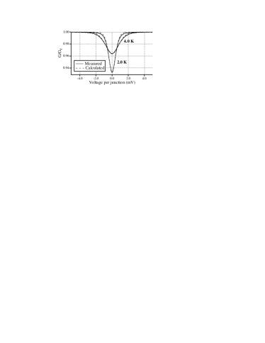
FIG. 1: The differential conductance as a function of bias voltage shows a
bell-shaped dip around zero voltage. These measurements were made on a
junction 2D-array with a resistance of 17 k
and an effective capacitance of 2 fF. The calculated curves were
calculated with higher order corrections [4].
We have measured current-voltage characteristics on a 2D array of
tunnel junctions at temperatures from 1.5 K to 4.2 K in a pumped
4He cryostat. Using the formulas derived for 1D-arrays we have
calculated the temperatures from these IV-curves and compared them
with temperatures calculated from the pressure of the He gas in the
cryostat. The correspondence is very good.
We have also made Monte-Carlo simulations of 1D- and 2D-arrays and these
simulations show that the tunnel junction capacitance which is
used in the equations for 1D-arrays should be replaced in the 2D case
by an effective capacitance which is higher than the real
capacitance.
II. Theory
The differential conductance of a 1D-array of junctions has been
calculated theoretically [1] to first order in the limit
. For arrays where all junctions have the same
resistance and capacitance and negligible capacitance to ground, the
result is
(1)
where the parameters and are defined as
(2)
(3)
is the differential conductance at voltages far above the
Coulomb blockade. The effective charging energy, is defined
similarly to the usual charging energy, except the physical capacitance
is replaced with the effective capacitance (which in a 1D-array with
negligible capacitance to ground is ).
The half-width of the resulting conductance dip depends
only on and :
(4)
The depth of the conductance dip also
depends on the effective capacitance of the junctions.
At low temperatures () higher order corrections should
be included [4]. This gives a correction
to the halfwidth in equation (4), which is independent of
temperature:
(5)
III. Sample parameters
The measured array consisted of tunnel junctions in a square
pattern with a side of 200 m and the area of the overlap
junctions was approximately 150 nm squared. The tunnel junctions
were made of aluminium with a tunnel barrier consisting of aluminium
oxide, AlOx, fabricated with standard shadow evaporation technique
[7, 8]. The junctions had a tunnelling resistance of
17 k and a capacitance of 1.1 fF which means was
0.85 K. The capacitance was calculated from the offset voltage,
=9.0 mV, using the offset analysis method described
in ref [5]. We have furthermore assumed that the offset
voltage of a 2D-array of tunnel junctions is [6].
FIG. 2: Comparison between the temperature calculated from the
half-width of the Coulomb blockade in the IV-curve and the
temperature calculated from the 4He equilibrium pressure.
IV. Experimental setup
The measurements were carried out in a pumped 4He cryostat which
has a temperature range from 4.2 K down to approximately 1.2 K. A
custom built biasing and amplification box fed the source signal to
the sample and amplified the current and voltage signals, which were
measured with two Keithley 2000 multimeters. A computer controlled
Keithley 213 voltage source was used for the voltage sweep. The
4He bath pressure was measured by a Wallace & Tiernan FA129 analog
pressure meter which was connected directly to the pumped helium space.
V. Results
We measured IV-curves at 50 different temperature points and
differentiated them numerically. Using equation 5 we
calculated the temperature and compared it with the temperature
calculated from the 4He equilibrium pressure in the He bath, using
the definition of ITS-90 [9]. As can be seen in figure 2 the
two temperatures are almost the same, but not quite. The temperature
from the IV-curve is consistently slightly higher than the temperature
from the 4He pressure.
The difference is clearer if we plot the relative difference,
i.e. (figure 3).
We see that there is a positive difference of 1-3% in all the
measurements. The uncertainty in the pressure readings was estimated
to about 1 Torr and the resulting temperature uncertainty is also
shown in figure 3. While it may account for some of
the spread, it can not explain the systematic difference of about 2%. One
possible explaination could be that the IV-curves were measured quite
rapidly one after the other, and perhaps the sample did not quite cool down
at each temperature before the measurement was made.
FIG. 3: The relative difference between the temperature calculated
from the IV-curve and from the 4He pressure. There is a systematic
difference of around 2%. As a comparison the uncertainty from the pressure
reading is included, but it can’t account for all the difference in
temperature.
We have made Monte Carlo simulations of one- and two-dimensional
tunnel junction arrays with a program package called simon[10] which is intended for simulations of circuits with very
small tunnel junctions. Because this method turned out to be very
time-consuming, we settled for quite small arrays, only three
junctions in series and two in parallel. Both 1D and
2D arrays behaved according to theory, except that in
the 2D case the capacitance in equation 2 was not the actual
capacitance of the tunnel junctions, but an effective capacitance
which was approximately 1.4 times the actual value in the
junction array. This is not surprising, though, since two
islands are not only connected via the junction between them, but also
via the other islands in the array. In an infinite 2D array the
capacitance between two neighbouring islands is exactly twice the
capacitance of the tunnel junctions, and this is the reason that the
offset voltage is a factor of two lower in a 2D-array compared to a
1D-array [6]. By calculating the effective capacitance from
we get , which
is twice the capacitance calculated from the offset voltage, as
expected.
An important property of the 2D-array is that it can be fabricated
with lower resistance than a 1D-array, even if it contains many
junctions in series. This means that the measurement can be done faster
and the measurement error is lower. When deducing the temperature from
the half-width of the conductance vs voltage curve, the uncertainty in
T depends both on the uncertainty in G and in V. The measurement
uncertainty can be written
(6)
(7)
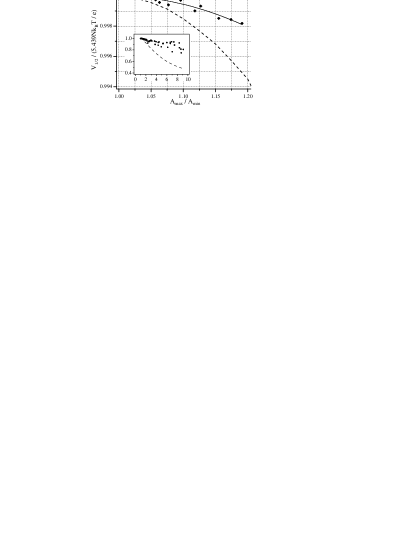
FIG. 4: The simulated half-width voltage, scaled by the ideal value,
plotted against (dots) for a
junction array. and
are the maximum and minimum junction areas respectively. The dashed
lines are the corresponding results for 1D-arrays by Hirvi et
al.[11], and the solid line is a quadratic fit to the
simulated values, to compare with the quadratic dependence in the
1D-array. It is clear that 2D-arrays are less affected by variations
in the tunnel junction areas than 1D-arrays, both at moderate
(big figure) and large (inset) variations. Larger arrays give
essentially the same result.
where and are the current and voltage
uncertainties respectively, given by the array resistance and
temperature, and the amplifier noise. and are
the intervals used for the numerical differentiation of the IV-curves
or, if lock-in measurements are used, the modulation ampliture. Note that
where is the differential
conductance at the half-width voltage. The last term in eq.
7 is the maximum differentiation error. Equation 7 has
a minimum with respect to and we can chose (in
our case approximately 5 % of ) to minimise the total error:
(8)
is the tunnelling resistance per junction at the
halv-width voltage. Note that the uncertainty decreases both with
increasing and .
Now we want to compare the measurement uncertainty of a 1D-
and a 2D-array. In this example we use a typical 1D-array of 30
junctions (typical because this is the approximate size used by Pekola
et al.), each junction with an effective capacitance of 2 fF
and a resistance of 20 k. For the 2D-array we assume
junctions and the same junction parameters. The temperature is 4 K. For
the measurement we assume AD743 operational amplifiers at the input stage,
because they have low voltage noise. The resulting uncertainty is
for the 1D-array and for the
2D-array, i.e. five times lower in the 2D case. One might
argue that we would get the same effect if we fabricated 256 parallel
1D-arrays with 256 junctions each, but then we might just as well make
it 2D, for the sake of robustness, as discussed earlier.
Another important issue is the tolerance to variations in the tunnel
junction properties. Since no fabrication process is perfect, small
variations can always be expected and in general, the smaller the
structures, the bigger are the relative differences. Hirvi et
al. have calculated the measurement error which can be expected in a
1D-array at different inhomogenities [11]. We have simulated
a junction 2D-array with random distributions of tunnel
junction areas and plotted the resulting half-width voltage
against the parameter
, where and
are the maximum and minimum junction areas
respectively (figure 4). Increasing the number of
junctions give essentially the same result. We have assumed that
for all junctions, which
follows from uniform tunnel barriers. It is clear from the figure
that the 2D-array is much less affected by variations in the junction
areas than 1D-arrays. For example, at a 10% spread
() the error in a 1D-array is
0.15%, while in a square 2D-array it is 0.05%. It
should be noted that even a -array is significantly better
than a 1D-array in this respect, at 10% spread the error is
0.08%.
VI. Conclusions
We have shown that a 2D-array of tunnel junctions can be used as a
primary thermometer in the same manner as 1D-arrays demonstrated
earlier. 2D-arrays have certain advantages over 1D-arrays for this
application, namely the robustness to damage of individual tunnel
junctions, higher tolerance to variations in tunnel junction
properties, lower signal noise and lower resistance which enables
faster measurement. This should make them more suitable for
temperature measurements at temperatures above a few hundred mK where
the electron heating effect is not a big problem. At lower
temperatures 1D-arrays are probably better, since the topology of
1D-arrays allow big cooling fins to be attached to the metal islands
of the array, and this will improve the thermalisation of the electron
system [12].
Acknowledgements
We thank Jari Kinaret, Jukka Pekola and Juha Kauppinen for fruitful
discussions. The Swedish Nanometer Laboratory was used to fabricate
the samples. This work was supported financially by the Swedish
foundation for strategic research (SSF) and by the European Union under
the TMR program.
References
[1] J. P. Pekola, K. P. Hirvi, J. P. Kauppinen and
M. A. Paalanen, Phys. Rev. Lett. 73, 2903 (1994).
[2] D. V. Averin, K. K. Likharev, in Mesoscopic
phenomena in solids, ed. B. Al’tshuler, P. Lee and R. Webb,
isbn 0-444-88454-8 (Elsevier, Amsterdam, 1991), p. 173.
[3]Single charge tunneling, Coulomb blockade
phenomena in nanostructures, ed. H. Grabert and M. Devoret,
isbn 0-306-44229-9 (Plenum, New York, 1992).
[4] Sh. Farhangfar, K. P. Hirvi, J. P. Kauppinen,
J. P. Pekola, J. J. Toppari, D. V. Averin and A. N. Korotkov, J. Low
Temp. Phys. 108, 191 (1997).
[5] P. Wahlgren, P. Delsing and D. B. Haviland,
Phys. Rev. B 52, 2293 (1995).
[6] N. S. Bakhvalov, G. S. Kasacha, K. K. Likharev and S. I.
Serdyukova, Physica B 165&166, 963 (1990)
[7] Jürgen Niemeyer, PTB-Mitteilungen 84, 251 (1974).
[8] G. J. Dolan, Appl. Phys. Lett., 31, 337 (1977).
[9] H. Preston-Thomas, Metrologia, 27, 3 (1990).
[10] Christoph Wasshuber, About single-electron
devices and circuits, Dissertation thesis, isbn 3-85437-159-4,
(Österreichiser Kunst- und Kulturverlag, Wien, 1998).
[11] K. P. Hirvi, J. P. Kauppinen, A. N. Korotkov, M. A.
Paalanen and J. P. Pekola, Appl. Phys. Lett 67, 2096 (1995)
[12] J. P. Kauppinen and J. P. Pekola, Phys. Rev. B
54, 8353 (1996).