Forschungszentrum Karlsruhe, Institut für Nanotechnologie, D-76021 Karlsruhe, Germany
Electronic transport in mesoscopic or nanoscale materials and structures Coulomb blockade; single-electron tunneling General theory, scattering mechanisms
Influence of nano-mechanical properties on single electron tunneling: A vibrating Single-Electron Transistor
Abstract
We describe single electron tunneling through molecular structures under the influence of nano-mechanical excitations. We develop a full quantum mechanical model, which includes charging effects and dissipation, and apply it to the vibrating C60 single electron transistor experiment by Park et al. [Nature 407, 57 (2000)]. We find good agreement and argue vibrations to be essential to molecular electronic systems. We propose a mechanism to realize negative differential conductance using local bosonic excitations.
pacs:
73.63-bpacs:
73.23Hkpacs:
72.20DpIntroduction. Experiments on electronic transport through nano-scale systems show a variety of physical conduction mechanisms. Due to their small size quantum mechanics becomes important and Coulomb blockade, interference, and Kondo physics are observed. Molecular systems [1, 2, 3, 4, 5, 6, 7, 8] are characterized by large electronic energies beyond room temperature and therefore offer the possibility to measure positions of molecular orbitals by transport spectroscopy. Furthermore, mechanical degrees of freedom in molecules have energies of order meV which can be probed experimentally for temperatures in the Kelvin regime. This letter addresses the latter topic and combines nano-electronic with nano-mechanical properties, in particular we model the experiment in Ref. [9]. We find that local bosonic excitations have an important influence on single electron tunneling, and thus need to be included in models for molecular electronics. Based on those systems we propose another way to realize negative differential conductance (NDC).
Attempts to model transport through molecular nano structures up to now focused more on the electronic structure[10]. In this letter we go one step further and include molecular vibrations (or any other local bosonic excitation) as well. We remark that our approach is fundamentally different from models where the vibration serves as a shuttle for the electrons[11, 12]. We address the case where the vibrational frequency is several orders of magnitude larger than the frequency associated with tunneling events. Moreover the physics is dominated by charging effects, therefore the single charge tunneling picture[13] is more appropriate than the scattering picture[14].
Experiment. In their experiment Park and coworkers measured the current through a single C60 molecule. Using a break junction technique they placed the molecule between two gold electrodes, to which it is weakly bound, i.e. the molecule sits in a Lennard-Jones-like potential on the gold surface. They could vary the source-drain and a gate voltage, that shifted the lowest unoccupied molecular orbital (LUMO). Thus they have built a C60 single electron transistor (SET). We briefly summarize their findings. The I-V curve displayed a large conductance gap, which could be varied with the gate voltage. Once the current was flowing a series of equally spaced ( meV) little jumps followed, which was attributed to the vibrational excitation of the whole molecule (center of mass motion) in the Lennard-Jones potential discussed above. More excitations at higher energies could also be found and could be attributed to e.g. intra-molecular vibrations. The experiment was conducted at K meV, the charging energy exceeded meV, and the separation of the LUMOs is assumed to be of similar magnitude. From the current one can deduce the tunneling broadening to be of eV.
Theoretical Model. Our model describes the dynamics of a local system, consisting of the electronic states and a single-mode bosonic excitation due to the harmonic potential, which accounts for the vibrations. The local system is coupled to two electronic reservoirs, a boson bath, which allows for dissipation and a gate that can shift the position of the MOs, see Fig. 1. Hence the Hamiltonian reads
[scale=0.33]system.eps
| (1) |
The electronic reservoirs are described by non-interacting electrons with a constant density of states , hence , where labels the left and right electrode and the spin. The bosonic reservoir is given by . The charging energy and the separations of the MOs is large enough to take the LUMO as the only participating MO. For the following discussion we take the LUMO to be spin-degenerate, and include the Coulomb interaction in a Hubbard-like charging term. With a projection operator for the vibrational states we have
| (2) |
The gate electrode is hidden in the dependence of on the gate’s potential. The energy levels of the oscillator are . The coupling to the boson bath ensures relaxation and dissipation of the vibrational energy in a natural way, and is generically written as
| (3) |
For simplicity, the constants are assumed to be independent of and we introduce the coupling via the spectral density . The exponent depends on the underlying microscopic realization of the boson bath, i.e. acoustical phonons, fluctuations in the electro-magnetic environment, etc. In the spirit of the Caldeira-Legett model[15], we assume from now on an Ohmic bath, i.e. . Finally the tunneling term, which includes the possibility to excite the whole C60 molecule to a vibration against the surface during a tunneling event,
| (4) |
Here, describes the tunnel matrix element in the absence of vibrational states, and the factor accounts for vibrational excitations. Their microscopic origin can be understood[9] similar to what is known as the Franck-Condon principle: The electron tunnels faster than the molecule can relax into a new state. When one electron tunnels onto the molecule, it is likely that the charge distribution around it, i.e. the image charges in the gates which serve as capacitors, is not uniform. Consequently there will be a force acting upon the charged C60. Hence the potential minimum is shifted slightly by a distance . Therefore we need the matrix elements between the states in the potential centered at and the states of the potential shifted by the distance , i.e. . For the system under consideration the states are well described by the harmonic oscillator ones. Obviously it gives for or zero for large, and we find that only a few transitions have considerable weight. With the tunneling broadening , we introduce the couplings and , which control both the current and the excitations.
Theory. The dynamics of the LUMO and all local bosonic excitations can be captured by a kinetic equation for the reduced density matrix, which is obtained by tracing out the reservoir and bath degrees of freedom of the full density matrix. For the parameters of interest double occupancy and off-diagonal matrix elements can be neglected ( and ). Then only the rates describing electron tunneling including vibrational excitation, and those related to bosonic transitions are required. Note that they are completely distinct, since the charge on the molecule changes by one for the electronic ones, and remains constant for the boson-mediated ones. For weak tunneling and weak dissipation , we can perform perturbation theory in the coupling constant in both cases. The rate describing a transition from zero charge and vibrational state to charge one with spin and vibrational state is given by with
| (5) |
For the reverse process the Fermi function will be replaced by . The rate describing phonon absorption and an accompanying vibrational excitation from to (without change of the electronic state) is given by
| (6) |
For the emission rate the Bose function is replaced by . The kinetic equation for the probabilities of the state reads , and the current is obtained via
| (7) |
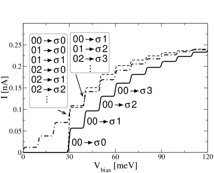
Results and Discussion. Before we focus on the specifics we discuss the general properties of the I-V characteristics. We tune the gate voltage such that the LUMO is above the Fermi levels. The voltage is applied symmetrically, i.e. . For low boson temperatures (solid curve in Fig. 2), absorption of phonons is suppressed and spontaneous emission, which in many molecules happens on a shorter time scale than the electron tunneling[16], will force the molecule to stay predominantly in its vibrational ground state. In this case, as in the experiment, we see no current until followed by a series of small steps with distance . The latter are due to excitations of higher vibrational states while tunneling. Each time the bias voltage exceeds , a new tunneling-in process can occur leading to an increase of the current. The excited vibrational state relaxes immediately to the ground state and tunneling-off happens via the process . The number of steps is determined by the number of vibrational states taken into account. The width of the rise for each single step is controlled by , which in our case is . In Fig. 2 we show results where all vibrational states can be accessed equally, i.e. . We remark that our results for strong dissipation are not special for the Ohmic bath, but rather independent of (positive) , since the energy is dissipated immediately.
The situation is more complicated in the absence of dissipation (dashed curve in Fig. 2). Here, once the threshold for the onset of current has been reached, the tunneling-off processes , with , can leave the initially not excited molecule in an excitated state. This state then serves as a starting point for other tunneling-in processes , with , leading to an increase of the current compared to the case with dissipation (after each additional step in the I-V-characteristics, the allowed values for increase by one).
For high boson temperatures where emission and absorption of phonons is possible (dot-dashed curve in Fig. 2), the I-V curve for is similiar to the case without dissipation. However, below the treshold, current precursors occur due to tunneling-in processes where the vibrational state lowers its energy. The higher vibrational states have here a finite probability due to absorption of phonons which is not possible in the absence of dissipation. However, since this is not seen in the experiment, one can rule out such high boson temperatures.
Experimentally the number of steps that can be resolved is much less than and we therefore proceed by taking into account the dependence of the Franck-Condon factor on the vibrational states. Assuming that the potential is well described in a harmonic approximation with parameters from the Lennard-Jones potential[17], then only the shift is unknown. A crude estimate, based on the force due to an image charge in the electrode, is given by Park et al [9]. Going beyond this picture is difficult because the electrodes’ geometry is not known. However, our results show that a better estimate may be obtained. In Fig. 4 we show the I-V characteristics for three ’s of the order of the previous estimate of pm. The ratio of the first and second step height is highly sensitive to . Comparing with the experiment one therefore would suggest a value of pm. Moreover it can be seen that the current saturates much faster than without Franck-Condon factors. This is not surprising, because the molecule is mostly in its ground state from which the higher states can not be reached. This is different without dissipation, where even a small NDC can be realized. The differential conductance, which shows a peak for every excitation, is shown in Fig. 4, with the NDC effect in the inset.
[width=7cm]fc_delta.epsdIdV.eps
We remark that our results agree very well with the experimental data[9]. However, there remain features which can not be reproduced in our calculation, namely a rising background and more excitations at higher energies. The origin of the background is not precisely known yet, the other excitations will be addressed below.
The NDC effect as seen before is due to a new mechanism specific for additional bosonic degrees of freedom. To exhibit the physics, Fig. 6 shows the effect for a simplified model of one electronic level with two vibrational states . The currents of the two plateaus are (for )
| (8) |
In the limit we see that only is needed to observe NDC. For , we get . The origin is that for the second plateau the probability distribution changes such that even weakly coupled vibrational states are occupied equivalently to the strongly coupled ones. However, their contribution to the current is small, and therefore the current decreases. We stress that the naturally show the appropriate kind of behavior. Assuming a simple functional form for them we show in Fig. 6 how many bosonic levels can in principle lead to large peak to valley ratios. For multi-mode bosonic excitations the effect survives and can even be more drastic, when many excitations are energy degenerate. NDC has already been seen in other nanostructures[18, 19, 20], and explanations in terms of spin-blockade[21] and asymmetric coupling[22] have been suggested. In our case however, no additional electronic states at higher energies are required, nor do we need the full many-body state of the structure.
[scale=0.28]ndc.epsndc_many.eps
Finally we comment on the influence of bosonic excitations in general molecular electronic devices. Multi-mode bosonic excitations can be included in the same way. Other degrees of freedom could be due to internal vibrations, e.g. the torsional vibration of the oligo-phenyl molecules used in the experiment by Chen and coworkers[20] have energies in the meV range and should be observable at low enough temperatures. The structure of smaller bosonic excitations would display itself on top of the larger ones, provided they are well separated. For heavier molecules where we expect for an interesting interplay including interference effects between the various excitations, partly related to off-diagonal elements of the density matrix. In addition, for , this can lead to an increasing background vibrational noise. This background (not in the gap) is indeed seen in the experiments and it is quite likely that such small local bosonic excitations play an essential role in it. We remark that this kind of behavior is fundamentally different from artificial semiconductor nano structures, which are embedded in a substrate.
Summary. We described single electron tunneling through a system with local bosonic degrees of freedom and dissipation to external heat baths. We applied our model to a C60 molecule, which can be excited to center of mass oscillations. We found that our results compare well with the experiment. We showed that this model may be used to realize negative differential conductance. We concluded that transport through molecular nano-devices is inevitably controlled by its electronic and mechanical structure.
Acknowledgements.
We would like to thank Filipp Furche, Matthias Hettler, Silvia Kleff, Gerd Schön and Florian Weigend for valuable discussions. This work is supported by the DFG as part of the Graduiertenkolleg ”Kollektive Phänomene im Festkörper” (D.B.) and via ”SFB 195” (D.B. and H.S.).References
- [1] \NamePersson S. H. M., et al. \REVIEWAppl. Phys. Lett.7419992546
- [2] \NameBezryadin A., et al. \REVIEWAppl. Phys. Lett.7119971273
- [3] \NameKlein D. L., et al. \REVIEWNature3891997699
- [4] \NameReed M. A., et al. \REVIEWScience2781997252
- [5] \NameZhou C., et al. \REVIEWAppl. Phys. Lett.711997611
- [6] \NameChen J., et al. \REVIEWScience28619991550
- [7] \NamePorath D., et al. \REVIEWNature4032000635
- [8] \NameKergueris C., et al. \REVIEWPhys. Rev. B59199912505
- [9] \NamePark H. et al. \REVIEWNature407200057
- [10] \NameDi Ventra M., Pantelides S. T. Lang N. D. \REVIEWPhys. Rev. Lett.842000979
- [11] \NameGorelik L. Y. et al. \REVIEWPhys. Rev. Lett.8019984526
- [12] \NameErbe A., Blick R. H., Tilke A., Kriele A. Kotthaus J. P. \REVIEWAppl. Phys. Lett.7319983751; \NameErbe A., Weiss A., Zwerger W. Blick R.H. \Reviewcond-mat/0011429
- [13] \NameSchoeller H. \BookMesoscopic Electron Transport, \EditorL. L. Sohn et al. \PublKluwer \Year1997; \NameKouwenhoven L. P. et al., ibid.
- [14] \NameLandauer R. \REVIEWIBM J. Res. Dev.11957223; \NameBüttiker M. \SAME321988306
- [15] \NameLegett A. J. et al. \REVIEWRev. Mod. Phys.5919871
- [16] \NameSalam G. P., Persson M. Palmer R. E. \REVIEWPhys. Rev. B49199410655
- [17] The molecule sits in the combined potential of the two electrodes, which are so close together that a binding energy of about eV can be assumed. The minimum is about Å away from the surface from which the energy meV can be deduced. See also \NameChavy C., Joachim C. Altibelli A. \REVIEWChem. Phys. Lett.4121993569; \NameRuoff R. S. Hickman A. P. \REVIEWJ. Phys. Chem.9719932494
- [18] \NameJohnson A. T. et al. \REVIEWPhys. Rev. Lett.6919921592
- [19] \NameWeis J., Haug R. J., v. Klitzing K. Ploog K. \REVIEWPhys. Rev. Lett.7119934019
- [20] \NameChen J., Reed M. A., Rawlett A. M. Tour J. M. \REVIEWScience28619991550
- [21] \NameWeinmann D., Häusler W., Pfaff W., Kramer B Weiss U. \REVIEWEurophys. Lett.261994467
- [22] \NameHettler M. H. Schoeller H. \Reviewcond-mat/0011047