Superconducting Gap Anisotropy in Nd1.85Ce0.15CuO4: Results from Photoemission
Abstract
We have performed angle resolved photoelectron spectroscopy on the electron doped cuprate superconductor Nd1.85Ce0.15CuO4. A comparison of the leading edge midpoints between the superconducting and normal states reveals a small, but finite shift of 1.5-2 meV near the (,0) position, but no observable shift along the zone diagonal near (/2,/2). This is interpreted as evidence for an anisotropic superconducting gap in the electron doped materials, which is consistent with the presence of -wave superconducting order in this cuprate superconductor.
pacs:
PACS numbers: 79.60.Bm, 73.20.Dx, 74.72.-hIt is now generally agreed that the hole doped (-type) cuprate superconductors have an order parameter whose majority component is of symmetry. Angle resolved photoelectron spectroscopy (ARPES) has provided a key piece of early evidence by the demonstration of a large momentum space anisotropy of the electronic excitation gap[1]. Quantum interference devices have given a definitive attestation to the existence of an order parameter that changes sign in momentum space[2]. Corroborating evidence has been provided by a number of other techniques[3].
In contrast, the experimental and theoretical situation on the small family of electron-doped (-type) cuprate superconductors[4], such as Nd1.85Ce0.15CuO4, has not reached a similar dtente. Tunneling[5], microwave penetration depth[6], and Raman [7] measurements all yield evidence for some kind of nearly uniformly gapped Fermi surface. In addition, Nd1.85Ce0.15CuO4 is the only measured cuprate superconductor that does not exhibit the so-called zero-bias Andreev bound state on its (110) surface that has been interpreted as a consequence of a momentum space sign change in the superconducting order parameter[8, 9].
However, recent work has called this picture of a uniformly gapped Fermi surface into some doubt. There is evidence from measurements using scanning SQUID microscopy on tri-crystal films, that the electron-doped materials have an order parameter with a large -wave component[10]. In addition, there has been speculation that the ordering at low temperature of the free 4 moments on the rare earth Nd ions affects the usual microwave penetration depth measurements by altering the low temperature magnetic permeability[8]. A recent reanalysis of microwave data that incorporates a correction for the Nd spin ordering, as well as experiments on the related paramagnetic material Pr2-xCexCuO4 have been interpreted as being more consistent with a -wave scenario[11].
On the theoretical side, there have been problems reconciling the -wave experimental results with current models. As in the hole doped case, strong on-site Coulomb repulsion in the copper oxygen plane strongly favors an anisotropic order parameter that has positive and negative lobes.
We have recently restudied the Nd1.85Ce0.15CuO4 system using high resolution ARPES and found two distinct features in the low energy spectra, which contrasts with the behavior of the p-types with hole doping, where the systematics of the single low energy feature interpolates between the prototypical undoped insulator and the optimally doped superconductor[12]. In the case of Nd1.85Ce0.15CuO4, the spectra are dominated by a broad highly dispersive feature which resembles that found in the undoped insulator Ca2CuO2Cl2[13]. In addition, a weaker feature at lower binding energy (meV) is observed near the () position. These two features should not be viewed as deriving from seperate “bands” of independent origin, as they conspire together to give a Fermi surface with the expected Luttinger volume.
In this letter we focus on an energy scale much lower than that of our previous work[12] (below 5 meV). The central intellectual issue is the anisotropy of the superconducting gap, which should manifest itself in the ARPES spectra as a displacement of the leading edge to higher binding energy as a gap opens up.
The single crystals of Nd1.85Ce0.15CuO4 used in this study were grown by the traveling solvent floating zone method. Details of this growth can be found elsewhere[14].
ARPES measurements were performed at beamline 5-4 of the Stanford Synchrotron Radiation Laboratory. This system is a Scienta SES 200 electron spectrometer coupled to a normal incidence monochromator (NIM) that is capable of better than 10 meV energy resolution and 0.2 degree angular resolution. Data was taken in Scienta “Angle” mode, in which an entire 5.5∘ angular cut can be imaged simultaneously. The incident photon beam angle was at approximately 45 degrees to the sample surface with its polarization in the direction of the angular cuts. Samples are positioned by a custom sample manipulator that can be cooled below 10 K. The sample temperature was measured by a calibrated diode mounted near the measurement position. The temperature difference between the diode position and the actual measurement position was found to be negligible previously from measurements on another diode that had been mounted to a sample holder in a identical fashion to the samples.
All Nd1.85Ce0.15CuO4 measurements were taken with 16.5 eV photons, which has been found empirically to give a high photoionization cross-section. Samples were aligned by Laue diffraction prior to vacuum chamber introduction. Shiny flat surfaces resulted from cleaving the samples by the top-post method at 10 K. LEED was performed after the UPS measurments to check surface structure and quality. For each measurement set, the temperature was cycled a number of times to ensure repeatability and an absence of problems from surface ageing. No such problems were detected over the typical measurement time of 7 hours per k-space cut. To improve statistics of these intrinsically low signal experiments the same temperature spectra were summed together.
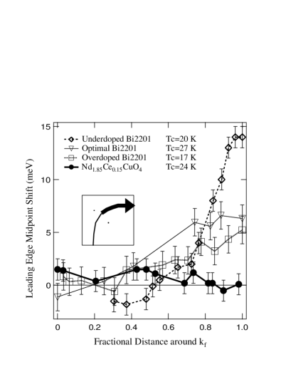
In order to see signatures of superconductivity on a system with an expected small gap, it is crucial that one compare leading edge midpoints (LEMs) from the same sample above and below Tc. In the past it has been standard practice to simply compare LEMs of the spectral weight onset to the Fermi energy of a reference gold sample, but this kind of analysis is not reliable in the small gap -type systems. To make this point more clear, in Fig. 1 we compare the trend of the LEMs of Nd1.85Ce0.15CuO4 referenced to the Fermi energy to that of one plane bismuth based cuprates with similar ’s as our Nd1.85Ce0.15CuO4 sample. All spectra were taken at approximately 11 meV resolution and with the polarization parallel to the Cu-O bond. The bismuth cuprate data is adapted from Ref.[15]. A few distinct trends are evident in the hole doped compounds. There is a notable decrease in the maximum gap as one proceeds from underdoping to overdoping. This is consistent with previous ARPES results as well as with other techniques. There is a definite increase in the LEMs as one goes around the Fermi surface in accordance with one’s d-wave expectation. Similar behavior is seen in YBa2Cu3O7-x and La1.85Sr0.15CuO4.[16, 17] In contrast, this analysis which reveals a large anisotropy on the hole doped compounds, does not reveal any clues as to anisotropy in Nd1.85Ce0.15CuO4 as the LEM referenced to shows no systematic trends along its Fermi surface. This is a consequence of the fact that the superconducting gap by any measure is much smaller than in the hole doped materials and hence is obscured due to finite resolution and subtle changes in the lineshape around the Fermi surface. If the systematics of the lineshape did not change very much around , one would still have a good measure of relative changes in the gap energy, despite not being able to measure its absolute magnitude exactly. This has been done, for example, in the imaging of a gap in Bi2212 and YBa2Cu3O7-x that follows the -wave functional form, despite large measured negative gap energies in the nodal region[16, 18]. In the present case, due to the previously mentioned weaker component that appears near () the systematics of the lineshape do change and a simple comparison with is not valid. One must then compare the shift of LEMs from spectra above and below Tc at the same momentum space point on the same sample in order to accurately measure the gap value. This should remove extraneous effects of the final state and otherwise eliminate effects (e.g. photoionization matrix elements) other than a gap opening up.
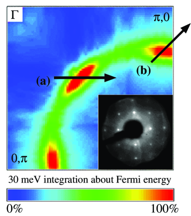
We took coarse energy resolution data at 10K with over 500 energy distribution curves (EDCs) over a Brillouin zone octant and symmetrized across the zone diagonal. Fig. 2 shows a 30 meV integration about the Fermi energy of these EDCs plotted over a Brillouin zone quadrant. Along the circularly shaped Fermi surface, one sees three regions of high intensity. The central one corresponds to the previously mentioned broad, highly dispersive feature moving into the integration window. The other two are the intensity maxima of the smaller low binding energy feature. In the inset is a typical low energy electron diffraction (LEED) pattern that shows bright well formed spots with a symmetry commensurate with that of the bulk. The extreme surface sensitive nature of LEED is an excellent cross-check of the surface quality. We took high resolution angle resolved cuts at two temperatures through points in two different regions of momentum space as shown by the arrows in the figure ( () and () exactly, but hereafter refered to as near () and () ). In both cases the photon energy was 16.5 eV, polarization was parallel to the cut direction, and the energy resolution was 11 meV.
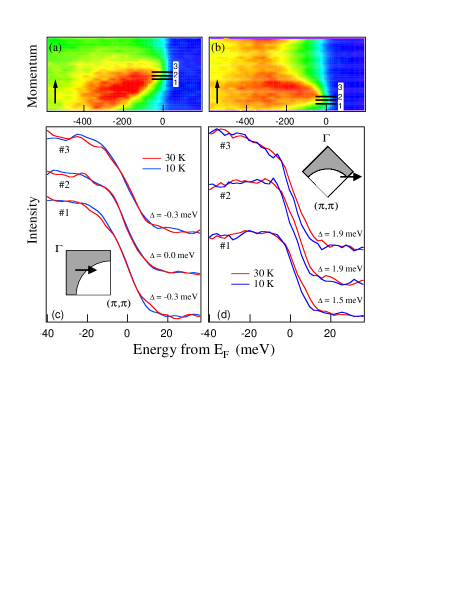
In Fig. 3a and 3b, we present color scale plots of the spectral function in a 5.5∘ ( ) angular windows from the cuts near () and () respectively. In the spectra near () we find a dispersion which is universal for the cuprates in this region of the Brillouin zone. A large broad feature disperses towards the Fermi energy, sharpens, and then disappears as it passes above EF. In 3b, which is a cut through at approximately (), the spectra are best characterized by a large hump feature that disperses only slightly while the smaller low energy feature disperses toward EF, loses weight, and then disappears. This behavior has been characterized in more depth elsewhere[12]. In Fig. 3c and 3d, we compare spectra at 0.5∘ steps taken at 30K (red) and 10K (blue) at a few near positions for each cut. In 3c from the spectra near () we see that, aside from some small thermal broadening, there is no temperature induced change. This is quite different from that of spectra from the crossing near () where there is a systematic displacement by 1.5-2meV of the leading edge to higher binding energy in the superconducting state.
In Fig. 4 there is an expanded image of a spectrum with one of the large temperature induced shifts in Fig. 3d. To more systematically quantify the result, we fit the lineshape with a simple phenomenological model. For broad spectral features at the Fermi level, the superconducting state spectra can be approximated by a 10K Fermi function multiplied by a linear spectral function whose onset edge is displaced from the Fermi energy by the superconducting gap energy. Likewise, the normal state spectra can be modeled as that of a 30K Fermi distribution at finite temperature multiplied by the same (but non-displaced) linear spectral function. These model spectra are convolved with a Gaussian of FWHM of 11 meV to simulate the experimental resolution. The agreement between the experimental curves and the fits are quite good within this picture with a gap parameter of 1.9 meV.
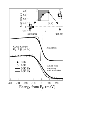
The above temperature dependent measurements were repeated on 7 different samples (4 samples at both positions, two only at ( and one just at () ). In the inset of Fig. 4 we plot the temperature dependent shift of the LEM at both crossings for all samples. Although there is some scatter in the data, one can see that, with the exception of one sample, they all show a 1.5-2 meV shift at the ( position and a negligible one at the () position. This shift anisotropy is interpreted as a consequence of the opening of a superconducting gap that is maximal near ( and minimal or zero along the zone diagonal. This is consistent with the presence of a d superconducting order parameter. However, we cannot rule out a very anisotropic -wave order with a small gap along the zone diagonal that is below our detection limit (approximately the same as the scatter in the data at (), ). The reason for the lack of a temperature dependent shift on the one sample is unknown. Its spectral features and dispersions were consistent with the others. It is possible that it suffered from being in poor thermal contact with the cold stage.
The 2 ratio in the narrow doping range of superconducting n-type materials is typically measured to be smaller than those in the hole-doped ones. There is no consensus on where they should fit analogously into the hole doped phase diagram, but perhaps the T2 dependence of their resistivity suggests that they are more overdoped-like. We may then expect a low 2 ratio. The gap value of 1.5-2 meV obtained with our technique is consistent with, but slightly smaller than, the gap values reported by other techniques[5, 6, 7]. There are a few possibilities for this. These other measurements typically take place at 4.2 K (0.15 Tc), in contrast to our measurement at approximately 0.5 Tc. At our intermediate temperatures the superconducting gap may not have opened fully. In addition, there may be some background contribution that partially obscures the gap signal. Lastly, it is well documented that photoemission analysis based on LEMs consistently underestimates the maximum gap value (in some cases by as much as a factor of 2) as compared to the intrinsic value defined as the quasiparticle energy at the antinodal position.[18].
In conclusion, we believe there is evidence for a anisotropic superconducting gap in the electron doped material that is consistent with a pairing state. Despite the strong differences between the and -type compounds in the larger scale electronic structure(1eV), their superconductivity appears to share the same symmetry and is therefore possibly of similar origin. The experimental data was recorded at the Stanford Synchrotron Radiation Laboratory which is operated by the DOE Office of Basic Energy Science, Division of Chemical Sciences and Material Sciences. Additional support comes from the Office of Naval Research: ONR Grants N00014-95-1-0760/N00014-98-1-0195. The crystal growth work was supported in part by Grant-in-Aids for Scientific Research from the Ministry of Education, Science, Sports, and Culture, Japan, and the New Energy and Industrial Technology Development Organization of Japan (NEDO).
REFERENCES
- [1] Z.-X. Shen et. al., Phys. Rev. Lett. 70, 1553 (1993);
- [2] J. R. Kirtley et. al., Phys. Rev. Lett. 76, 1336-1339 (1996); D. A. Wollman, D. J. Van Harlingen, J. Gianpintzakis, D.M. Ginsberg, Phys. Rev. Lett., 74, 797-800 (1995)
- [3] D.J. Scalapino, PHYSICS REPORTS 329-65 250, (1995) and references therein
- [4] Y. Tokura et. al., Nature 337, 345 (1989)
- [5] Q. Huang et. al., Nature, 347, 369-372 (1990)
- [6] D. Wu et. al., Phys. Rev. Lett., 70, 85-88 (1993); S.H. Wang et. al., Phys. Rev. Lett.,64, 1067-1070 (1990)
- [7] B. Stadlober et. al., Phys. Rev. Lett., 74, 4911-4914 (1995)
- [8] L. Alff, et. al., Phys. Rev. B, 58, 11197-11200 (1998)
- [9] S. Kashiwaya et. al., Phys. Rev. B, 57, 8680-8686 (1998)
- [10] C.C. Tsuei and J.R. Kirtley, Phys. Rev. Lett.,85, 182-185 (2000)
- [11] J.R. Cooper et. al., Phys. Rev. B, 54, no.6, R3753-5 (1996); J. D. Kokales et. al., Phys. Rev. Lett.,85, 3696 (2000); L. Alff, S. Meyer, S. Kleefisch, U. Schoop, A. Marx, H. Sato M. Naito, and R. Gross, Phys. Rev. Lett., 83, 2644-2647, (1999); R. Prozorov et. al., Phys. Rev. Lett.,85, 3700 (2000)
- [12] N. P. Armitage et. al., in preparation
- [13] F. Ronning et al., Science 282, 2067 (1998); B. O. Wells et. al., Phys. Rev. Lett. 74 964 (1995)
- [14] Y. Onose, et. al., Phys. Rev. Lett. 82 5120 (1999)
- [15] D.L. Feng, Z.-X. Shen, R. Yoshizaki, manuscript in preparation
- [16] M. Schabel et. al., Phys. Rev. B, 55, 2796 (1997)
- [17] T. Yoshida et. al., manuscript in preparation
- [18] A. Loeser et. al., Phys. Rev. B, 56, 14185 (1997)