A single-electron inverter
Abstract
A single-electron inverter was fabricated that switches from a high output to a low output when a fraction of an electron is added to the input. For the proper operation of the inverter, the two single-electron transistors that make up the inverter must exhibit voltage gain. Voltage gain was achieved by fabricating a combination of parallel-plate gate capacitors and small tunnel junctions in a two-layer circuit. Voltage gain of 2.6 was attained at 25 mK and remained larger than one for temperatures up to 140 mK. The temperature dependence of the gain agrees with the orthodox theory of single-electron tunneling.
pacs:
85.30.Wx, 73.23.HkThe use of single-electron tunneling devices for computation has been widely discussed because these devices can be made very small and they consume relatively little power. [1, 2] A variety of single-electron device logic schemes have been put forward but relatively few of the proposed single-electron logic elements have been tested experimentally. Here, measurements on a single-electron inverter are presented. The inverter is a fundamental building block of single-electron transistor logic, which bears considerable resemblance to standard Complementary Metal-Oxide-Semiconductor (CMOS) logic. [3, 4] The logic levels are represented by voltages and a small number of electrons are transported when the inverter switches from the high state to the low state. The logic gates NAND and NOR can be realized by making slight variations on the inverter circuit. With two inverters, a static Random Access Memory (RAM) memory cell can be constructed and a ring oscillator can be made from three inverters. Voltage gain is essential for many of these circuit applications but thus far gain has been achieved in relatively few devices. [5, 6] The inverter discussed here has voltage gain.
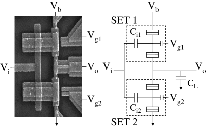
A scanning electron microscope (SEM) photograph of the device and a schematic diagram of the inverter circuit are shown in Fig. 1. The inverter consists of two nominally identical single-electron transistors (SET’s) in series that share a common input gate. Each single-electron transistor used in this inverter contains a small aluminum island with a total capacitance fF. The SET’s are outlined with dotted lines in the schematic. The input of the inverter, , extends under the two islands. The input is electrically isolated from the two islands by an 8 nm thick layer of aluminum oxide. This forms the two input capacitors and . The output is connected to ground via an on-chip load capacitor of 130 pF to suppress charging effects at the output. The output is also coupled to the two islands via small tunnel junctions. The power lead, , and the grounded lead are similarly connected to the islands via small tunnel junctions. The two tuning gates, and , are used

to tune the induced charges on the two islands. For inverter operation, the output should be high when the input is low and the output should be low when the input is high. This is achieved by applying a bias voltage of V and adjusting the two tuning gates such that when the input voltage is low, the top transistor is conducting and the bottom transistor is in the Coulomb blockade. This effectively connects the output to the supply voltage and makes the output high. The Coulomb blockade prevents a steady current from flowing through the inverter limiting the dissipation in this device. When a high input voltage is applied, this shifts the induced charge on each of the SET’s by a fraction of an electron and puts the top transistor in Coulomb blockade and makes the bottom transistor conducting so that the output is effectively connected to ground. Thus, when the input is high, the output is low.
The device was fabricated on a thermally oxidized silicon substrate using a high-resolution electron beam pattern generator at 100 kV. Each layer of the circuit was defined using a double layer resist and was aligned to prefabricated Pt markers. The bottom layer of the circuit consisted of a 25 nm thick aluminum film that was patterned to form the lower electrodes of the gate capacitors and the load capacitor. To form the dielectric for the capacitors, the sample was heated to 200∘C and the aluminum was oxidized in an O2 plasma at 100 mTorr for 5 minutes. The resulting AlxOy layer was 8 nm thick. A second aluminum film was then deposited in a pattern that defined the islands and the leads. The four tunnel junctions were defined in this layer by shadow evaporation.
The device was measured in a dilution refrigerator with a base temperature of 25 mK. All leads were equipped with -filters at room temperature and copper-powder filters at base temperature. Superconductivity was suppressed using a 1 T magnetic field. Measurements on the individual SET’s revealed that the tunnel junctions were all identical with capacitances of aF and resistances of 1.1 M. The input capacitances were aF and = aF, the tuning gate capacitances were aF, and the stray capacitance of each island was estimated to be aF.
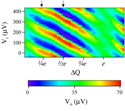
Figure 2a shows the dependence of the output voltage on and , the difference between the induced charge on both islands. The induced charge difference can be controlled by adjusting the two tuning gates and . This figure illustrates that the input-output characteristics of the inverter can vary greatly depending on the voltages applied to the tuning gates. In the region around , the output is a weak function of the input. When the tuning gates are adjusted so that the induced charges are out of phase, there are large oscillations of the output voltage as the input voltage is varied.

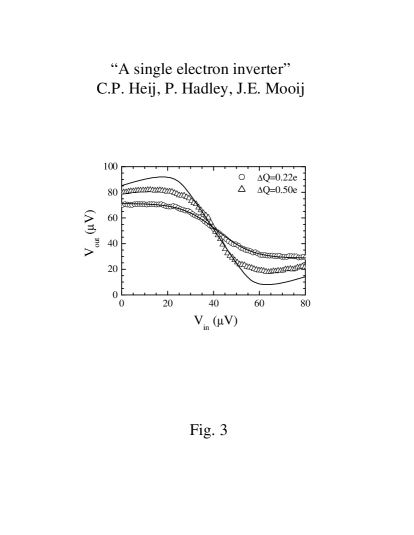
Increasing both of the tuning gates simultaneously leaves constant but has the same effect as increasing . Figure 3 shows input-output characteristics at 30 mK for two different values of . The arrows in Fig. 2 indicate where the data for Fig. 3 was extracted. Note that when the input voltage is low, the output voltage is high and when the input voltage is high, the output voltage is low. To achieve this input-output characteristic, the gate voltages were adjusted manually. At this point there is no procedure known for automatically tuning the gate voltages on-chip for the optimal inverter performance. This is probably the largest problem inhibiting the further development of this sort of logic.
The solid lines in Fig. 3 are simulations of the inverter characteristic calculated at 30 mK using the orthodox theory for single-electron tunneling. For the most part, the orthodox theory fits the measurements. The largest deviations occur at and either minimal or maximal output voltage. At , the maximal observed output voltage swing is 75% of what is expected from orthodox theory. This can be due to external noise coupling in via the leads. The device is most sensitive to external noise at these bias conditions.

An important consideration for the proper operation of an inverter is that the maximum output voltage swing must be greater than the voltage swing necessary at the input to switch the output from low to high. In other words, the inverter must exhibit voltage gain. The maximum voltage gain that can be achieved in a single-electron transistor is the ratio of the input-gate capacitance to the junction capacitance . In this work, overlap capacitors were used to make relatively large input-gate capacitors. The maximum voltage gain of the inverter, which can be determined from the slope of the transitional region in Fig. 3, was .

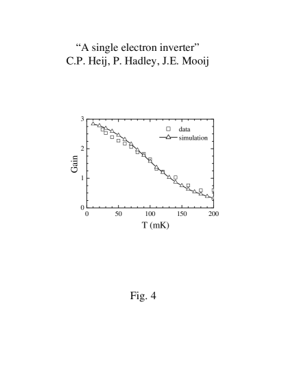
Figure 4 shows the gain of the inverter as a function of temperature. Note that a voltage gain greater than one is attained for temperatures below about 140 mK. This is the highest temperature for which voltage gain in a single-electron transistor has been achieved. While there have been many reports of single-electron transistors operating at room temperature, those transistors typically have a voltage gain much less than one. Gain is difficult to achieve at high temperatures because the gate capacitance must be made larger than the junction capacitance while making the total capacitance small. Fabricating a room-temperature single-electron transistor with voltage gain is challenging because it almost certainly requires control of the fabrication process on a nanometer scale in three dimensions.
The measurements on this single-electron inverter show that it can operate as it was designed to and that the orthodox theory adequately describes the behavior of the circuit. The voltage gain necessary for the operation of this inverter was achieved by using overlap capacitors in a multilayer circuit, yielding a maximum gain of 2.6 at 25 mK.
REFERENCES
- [1] For an overview of Single-electron devices and their applications, see: K. K. Likharev, Proceedings of the IEEE 87 606 (1999).
- [2] Yu. A. Pashkin, Y. Nakamura, and J.S. Tsai, Appl. Phys. Lett. 76 2256 (2000).
- [3] J. R. Tucker, J. Appl. Phys. 72 4399 (1992).
- [4] A. N. Korotkov, R. H. Chen, and K. K. Likharev, J. Appl. Phys. 78 2520 (1995).
- [5] G. Zimmerli, R.L. Kautz, and John M. Martinis, Appl. Phys. Lett. 61 2616 (1992).
- [6] C. P. Heij, D. C. Dixon, P. Hadley, and J. E. Mooij, Appl. Phys. Lett. 74 1042 (1999).