The fabrication of reproducible superconducting scanning tunneling microscope tips
Abstract
Superconducting scanning tunneling microscope tips have been fabricated with a high degree of reproducibility. The fabrication process relies on sequential deposition of superconducting Pb and a proximity-coupled Ag capping layer onto a Pt/Ir tip. The tips were characterized by tunneling into both normal-metal and superconducting films. The simplicity of the fabrication process, along with the stability and reproducibility of the tips, clear the way for tunneling studies with a well-characterized, scannable superconducting electrode.
I Introduction
Scanning tunneling microscopy (STM) has been proven to be an important tool in the study of superconducting materials by serving as a local probe of the density of states (DOS) near the Fermi energy.[1, 2, 3, 4] STM studies of superconducting materials are conventionally performed in the S/I/N (superconductor/insulator/normal-metal) configuration, where a sharp normal-metal tip is brought to within tunneling distance from a superconducting sample. A natural and intriguing extension of the capabilities of STM studies would be to use a superconducting tip, thus allowing for S/I/S measurements.
Although superconducting tips have been used in the past in an attempt to form S-S point contacts,[5] true vacuum tunneling has not been achieved until quite recently.[6] The difficulty in fabricating superconducting tips arises mainly from the conflicting needs of making an atomically sharp tip, while keeping the tip apex clean and well defined. Since most known superconducting materials readily oxidize, the fabrication of a superconducting tip is significantly more complicated than that of a normal-metal tip, where metals like Pt and Au can be used. In addition, one may be concerned that the tunneling current through a very small junction area may lead to current densities that are sufficient to destroy the superconducting state at the tip. This issue was addressed by Meservey who argued that currents, typical of normal STM operation, could be carried without excessive depairing. [7]
Pan et al. [6] have demonstrated that quasiparticle tunneling from a sharp superconducting tip is indeed possible. They have used tips cut from Nb wire and cleaned in-situ by field emission. Although the work of Pan et al. provided an important step towards the implementation of superconducting tips in STM studies, their method of tip fabrication did not yield sufficiently reproducible results, and a large variation in the superconducting properties of their tips was observed.[6] It may be argued that the field emission cleaning procedure used did not remove all of the Nb oxides from the tip. There are a variety of oxides in Nb, out of which NbO2 and Nb2O5 are insulators and their removal can be verified by successful tunneling at low temperatures. However, NbO is metallic at 4.2 K and any residue of this material on the tip apex, which is not directly detectable, may result in a proximity layer of unknown thickness. To our knowledge, no method for the fabrication of reproducible superconducting tips has been reported yet.
In this article we demonstrate a new, simple method for the fabrication of superconducting tips. By use of a controlled Pb/Ag proximity bilayer deposited onto pre-cut Pt/Ir tips, we have obtained superconducting tips with a high degree of reproducibility. Furthermore, due to the slow oxidation rate of Ag and the mechanical rigidity of Pt, our tips can be easily manipulated ex-situ without any significant degradation of their superconducting properties.
II Fabrication and characterization
Pt0.8/Ir0.2 tips were cut from a 0.25 mm diameter wire. We verified the quality of these tips by imaging the surface of a highly ordered pyrolytic graphite single crystal at room temperature. The tips with the best resolution were selected, and placed in a bell-jar evaporator such that the tip axis was pointing in the directions of the evaporation sources to prevent shadowing effects. A 5000 Å thick layer of Pb was deposited on the Pt/Ir tips by thermal evaporation at a rate of 50 Å/sec. Without breaking vacuum, a thin layer of Ag was subsequently evaporated at a rate of 2 Å/sec. The Ag layer thickness was varied from 30-60 Å in four different deposition runs. The pressure during the two-step evaporation process was 410-6 torr or lower.
Pb (Tc=7.2 K) was chosen so that at 4.2 K the tips would be well below their transition temperature and the layer thickness was chosen to assure bulk superconductivity in the Pb layer (=830 Å). The silver serves as a capping layer, protecting the lead from rapid oxidation upon exposure to the atmosphere. The thin Ag layer is proximity-coupled to the lead layer, and it has been
demonstrated[8] that the Pb/Ag proximity junction is reproducible and stable. The Pb-Ag combination is also a good metallurgical choice, as there is no significant alloying at the interface.[9] The tip is therefore expected to behave as an effective superconductor with Tc and only slightly below that of bulk lead.
We have found that our tips can be stored in air for a period of about two days before an oxide layer is formed, which is thick enough to prohibit tunneling at low temperatures. The lifetime of the tips can be appreciably extended when stored in rough vacuum, and we have successfully used tips after three weeks of storage under these conditions.
In order to characterize the tips, we have performed tunneling measurements on a Au sample in the temperature range 2.0-6.3 K, using a custom built ultra high vacuum low temperature STM.[4] Ultra high purity 4He exchange gas was used to thermally couple the STM to a liquid He bath, whose temperature could be lowered to 2.0 K by lowering the He vapor pressure. Measurements above 4.2 K were performed while the STM was allowed to slowly warm up. Differential conductance was measured using standard lock-in techniques. At each bias voltage sweep, 512 data points were taken at a rate of 3.0 ms per data point. Data was typically averaged over 250 (100) ramps below (above) 4.2 K. The junction resistance was 100 M with the bias voltage during the feedback cycle fixed at +50 mV with respect to the grounded sample. Since the Au sample is a normal metal with a constant density of states (DOS) near the Fermi energy, the obtained curves represent the tip DOS.
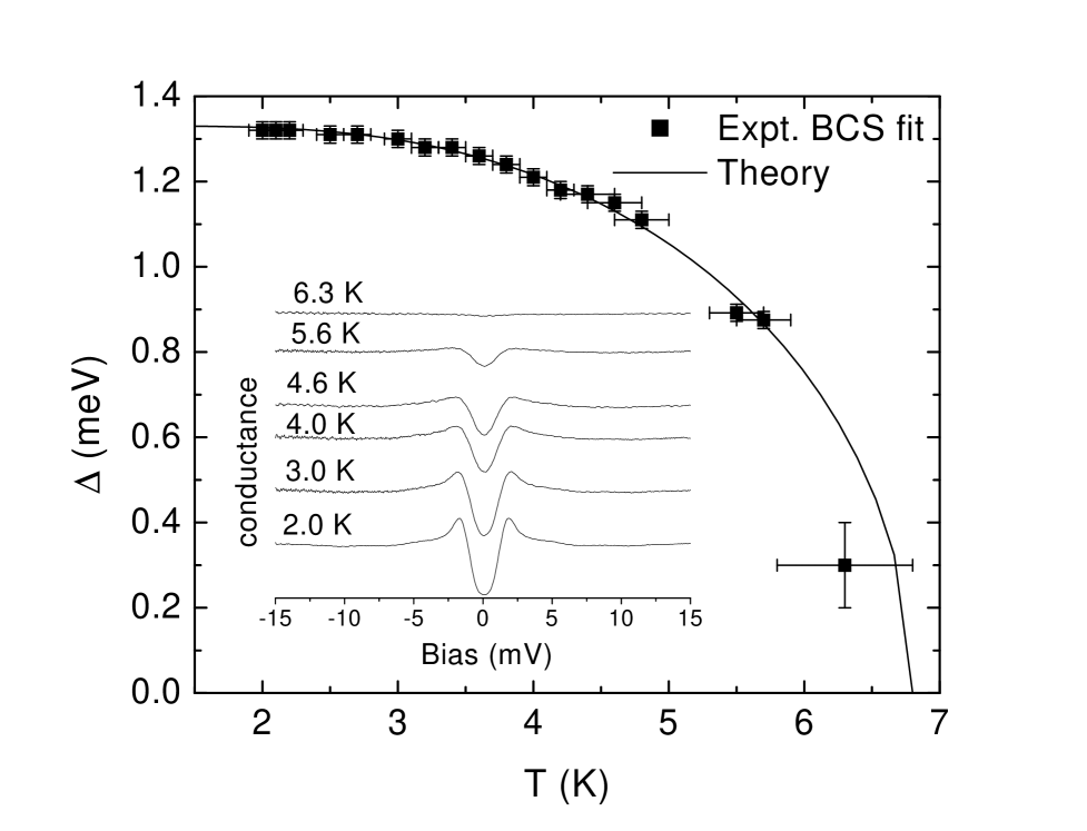
Typical results are presented in Figure 1. Conductance curves (shown in inset) were fitted to BCS theory using the Dynes, Narayanamurti, and Garno DOS,[10] allowing both and to vary, while the temperature was fixed to the value read by a thermometer mounted on the sample holder. We believe these values accurately reflect the
temperature of the tip, as thermal coupling through the exchange gas between the scanner head and the sample holder is good, and self-heating is ruled out.[11]
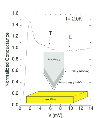
A superconducting gap is clearly seen below 6.3 K, and its evolution with temperature is very well described by the BCS theory.[12] We obtain =1.330.01 meV and Tc=6.800.05 K, yielding =4.540.05. The values of estimated from the fits increased steadily with temperature, from 0.16 meV at 2 K to 0.40 meV at 6 K. The values obtained for the gap for tips from the same fabrication batch were in good agreement with each other, while the variation of the gap value among tips from different batches did not exceed 10%, and was consistent with the slightly different Ag layer thicknesses produced in the separate depositions. Below T=3.0 K it was possible to resolve the lead phonon contribution to the tunneling DOS, which arises from the energy dependent order parameter due to strong electron-phonon coupling. The phonon structure is clearly seen around 2 K, and the obtained phonon energies and structure (Fig. 2) are in good agreement with the data in the literature.[13, 14] The fact that the phonon structure is clearly observed, together with the reproducibility of results for a range of junction resistances and the characteristic exponential dependence of the tunneling current on the tip-sample distance, is evidence that our tips form single-step vacuum tunnel junctions.
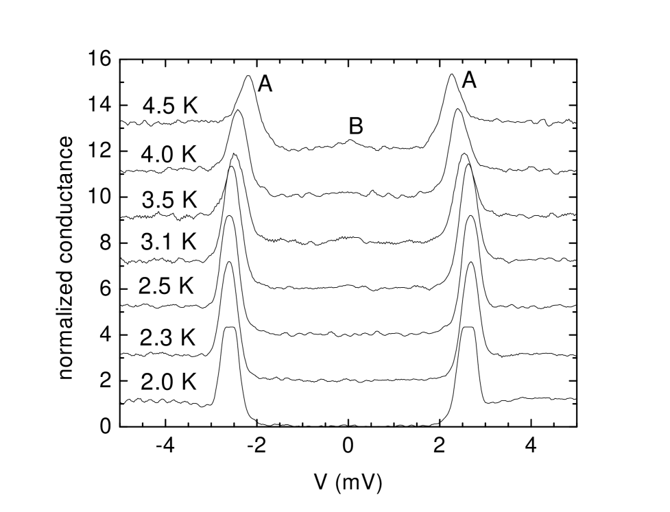
Figure 3 shows representative conductance spectra for vacuum tunnel junctions formed between our superconducting tips and a Pb film deposited in-situ on a graphite substrate. These spectra are characteristic of an S/I/S junction, and conductance peaks (A) are clearly visible at the expected voltages corresponding to eV=(). The peak corresponding to the gap difference (B) disappears, as expected, as the temperature is lowered and the number of available states due to thermal excitations across the gap is reduced. At higher temperatures this peak is located at zero bias, which confirms again that the superconducting gap value of the tip is very close to that of lead.
It is remarkable that the tip structure is conserved despite the relatively large amount of material deposited onto it. Since our STM is optimized for large area scans, and atomic resolution images are therefore not ordinarily obtainable, we can only give an estimate on the lower bound of the tip resolution. This was done by imaging the profile of step edges on graphite, and taking the apparent width of the step to be characteristic of our instrument resolution. Using this procedure we obtain resolutions of 5-20 Å. Since the growth of Pb is granular in nature it is reasonable to assume that the tip resolution is limited by the size of the Pb grain at the apex of the tip. Limiting the mobility of Pb atoms during the deposition, by using higher deposition rates, using a Ge seed layer, or by cooling down the tip during deposition, would decrease the Pb grain size and probably improve the tip resolution.
III conclusion
In summary, we have demonstrated a new method for the fabrication of superconducting tips. We have shown that this method, relying on proximity coupling between a Pb superconductor and Ag capping layer, is capable of yielding reproducible, clean, and stable tips with Tc and close to that of bulk Pb. The observed tunneling characteristics in both S/I/N and S/I/S configurations and their temperature dependence are consistent with expectations.
Many possible applications emerge from the availability of well characterized, reproducible superconducting tips, ranging from thermometry [6] to spin polarized tunneling [7]. Recently there has been increased theoretical interest in the use of superconducting tips for tunneling experiments into high-Tc superconductors[15, 16], where for example, information regarding the order parameter symmetry can be obtained by tunneling near a grain boundary in such materials [15].
Arguably, one of the most intriguing applications is the possibility of forming a scannable Josephson junction [16]. Because of the inherently high resistance of a vacuum tunnel junction, the Josephson coupling energy, E, where is the junction normal resistance, is expected to be smaller than or comparable to the thermal energy in the system. In this case, strong phase fluctuations will have a dominant effect on pair tunneling, as was shown by Ivanchenko and Zil’berman [17]. Preliminary studies have shown [18] that low temperature I-V curves for junction resistances around 50-100 k are in agreement with the theory of Ivanchenko et al.
To conclude, our newly developed tips may open the way to a variety of STM studies previously out of reach, most notable is the possibility for a scanning Josephson tunneling microscope.
Acknowledgements.
The authors would like to thank A. D. Truscott, O. Bourgeois, and F. Hellman. This work was supported by AFOSR Grant No. F49620-92-J0070, ONR Grant No. N00014-92-J1320, and NSF Grant No. DMR9705180.REFERENCES
- [1] S. H. Pan, E. W. Hudson, K. M. Lang, H. Eisaki, S. Uchida, and J. C. Davis, Nature (London) 403, 746 (2000).
- [2] Ali Yazdani, B. A. Jones, C. P. Lutz, M. F. Crommie, D. M. Eigler, Science 275, 1767 (1997).
- [3] Ch. Renner and Ø. Fischer, Phys. Rev. B. 51, 9208 (1995).
- [4] A. D. Truscott, R. C. Dynes, L. F. Scheenmeyer, Phys. Rev. Lett. 83, 1014 (1999).
- [5] see for example, J. G. Rodrigo, N. Agraït, S. Vieira, Phys. Rev. B. 50 374 (1994).
- [6] S. H. Pan, E. W. Hudson, and J. C. Davis, Appl. Phys. Lett. 73, 2992 (1998).
- [7] R. Meservey, Physica Scripta 38, 272 (1988).
- [8] A. S. Katz, A. G. Sun, R. C. Dynes, K. Char, Appl. Phys. Lett. 66, 105 (1995).
- [9] M. Hansen, Constitution of Binary Alloys, 2nd ed.(McGraw-Hill, 1958)
- [10] R. C. Dynes, V. Narayanamurti, and J. P. Garno, Phys. Rev. Lett. 41, 1509 (1978).
- [11] The power dissipated by quasiparticle relaxation is inversely proportional to the junction resistance. The observed dI/dV curves for different junction resistances are essentially identical, thus ruling out any significant self-heating of the tip. See also E. W. Hudson, Ph. D. Thesis, University of California, Berkeley, 1999
- [12] M. Tinkham, Introduction to Superconductivity, 2nd ed.(McGraw-Hill, New York, 1996)
- [13] J. M. Rowell, in Tunneling Phenomena in Solids, Ed. E. Burstein and S. Lundqvist (Plenum Press, New York, 1969)
- [14] Gerald B. Arnold, Phys. Rev. B. 18, 1076 (1978).
- [15] H. Zhao, and C.-R. Hu, Phys. Rev. B. 62, 1308 (2000).
- [16] J. Šmakov, I. Martin, and A. V. Balatsky, arXiv:cond-mat/0009310 (2000).
- [17] M. Ivanchenko and L. A. Zil’berman, Sov. Phys. JETP 28, 1272 (1969).
- [18] O. Naaman, W. Teizer, and R. C. Dynes, To be published