Negative differential resistance in nanotube devices
Abstract
Carbon nanotube junctions are predicted to exhibit negative differential resistance, with very high peak-to-valley current ratios even at room temperature. We treat both nanotube p-n junctions and undoped metal-nanotube-metal junctions, calculating quantum transport through the self-consistent potential within a tight-binding approximation. The undoped junctions in particular may be suitable for device integration.
pacs:
73.61.Wp, 85.30.Vw, 73.30.+y, 73.40.NsThe scaling of semiconductor devices to ever-smaller sizes is rapidly approaching fundamental limits, spurring the exploration of new materials. Carbon nanotubes (NTs) have particular appeal due to their small size and unique mechanical and electronic properties; and some NT devices have already been reported [1].
Recent theoretical work on NT devices has focused on simple operations such as rectification [2, 3, 4], based on thermal excitation of carriers over a potential barrier. However, in NT devices tunneling through the barrier can actually dominate the transport [2, 5]. Such tunneling currents can lead to negative differential resistance (NDR), with a wide range of potential device applications [6, 7].
Here we show that NT junctions are ideally suited to function as nanoscale NDR device elements. We consider two very different devices — a simple p-n junction, and an entirely new device structure based on metal contacts to an undoped NT. The latter device relies on the nanoscale lateral size of nanotubes and has no analog in bulk devices, illustrating the exciting possibilities that nanotubes present.
In both cases, the direct gap and long tunneling length of the NT contribute to a high peak current, while the strong carbon bonding and small device size reduce the likelihood of any defect levels in the bandgap contributing to excess valley current. Thus the predicted peak/valley current ratios exceed by orders of magnitude those seen in existing devices.
Nanotube p-n junctions have been studied before [2, 4, 8], although their potential as NDR devices has not been recognized. These simple devices provide an ideal testing ground for general ideas about device operation. For technological applications, however, one would prefer a device that does not require doping and that can be integrated into a multi-level architecture. The metal-NT-metal structure considered here has precisely these desirable attributes.
We first consider a p-n junction made with a semiconducting single-wall NT. Specifically, we treat a (17,0) zigzag NT with a radius of 0.66 nm. (See Ref. [1] for notation and a general description of the NT atomic structure.) Our qualitative results also apply to other semiconducting NTs. We use a tight-binding Hamiltonian with one orbital per carbon atom and a nearest-neighbor matrix element of 2.5 eV [9], giving a direct band gap of 0.55 eV. We consider NT junctions both in vacuum and embedded in a dielectric material ( 3.9).
Doping of NTs could be accomplished by insertion of atoms inside the tubes [10] or by substitution into the lattice [11], and we have considered both methods. We model dopants inside the tube by a line of charge on the tube axis, either positive for n doping or negative for p. (Replacing the line with discrete ions has negligible effect.) A reasonable packing density corresponds to highly degenerate doping, with an atomic doping fraction of about 0.01, and we use this value throughout our calculations. Substitutional doping can be modeled (within a sort of virtual-crystal approximation) by a uniform cylinder of charge on the tube. I-V curves calculated with these two models agree within 1-2% for all applied voltages.
We calculate the current using the method of Ref. [12]. The NT is divided into two semi-infinite “leads” and a “scattering region” 13.3 nm in length. Within the scattering region we use the full self-consistent potential , including applied bias and free-carrier screening. The potentials in the leads are taken as constant, and equal to the potentials at the boundaries of the scattering region; and the scattering region is taken long enough to assure the accuracy of this approximation.
To obtain , we self-consistently calculate the charge and potential for a periodically repeated cell of 26.6 nm, consisting of p and n regions of equal size. The local density of states on each atomic site is obtained by direct diagonalization of the Hamiltonian. The charge on each site is given by integration of the product of the local density of states and the Fermi function.
This standard method is only directly applicable in equilibrium, and must be adapted for the presence of an applied voltage. In the limit of large junction resistance (low current), the p and n regions are each in internal equilibrium, but with Fermi levels that differ by the applied voltage. We therefore calculate the charge using separate Fermi functions for the two regions. (There is a region near the junction where the Fermi level is undefined; but in the voltage range of interest, this region is fully depleted and contributes negligible free charge regardless of which Fermi level is used.) The accuracy of this approach is discussed further below.
For a given charge (including both electronic and ionic contributions), the electrostatic potential is , where is the electrostatic kernel for a cylinder [13] and is the NT radius. [For a tube embedded in a dielectric (), the formula neglects the presence of a hole in the dielectric. A more accurate calculation in the context of the metal-NT-metal device is presented below.] In our numerical procedure, we start from a charge and obtain ; the diagonal elements of the Hamiltonian are then shifted by , the electronic charge is re-calculated, and the procedure is iterated to self-consistency.
The tight-binding formalism gives only the total charge associated with a site. To calculate the potential, we must assume a particular spatial distribution of the site charge. In our calculation the charge associated with a “ring” of sites is distributed uniformly over a length of the NT cylinder. To test the sensitivity of the results to the spatial distribution, we vary from 0.05 nm to 0.5 nm, which includes all physically reasonable values. Over this large range the current varies less than 5%. We expect that the effect of varying the radial extent of the charge or lifting the approximation of cylindrical symmetry would be similarly minor.
The Landauer-Büttiker formula [12] gives current
| (1) |
Here is the electron transmission probability across the scattering region at energy , is the applied voltage, and the Fermi function. We keep only the first valence and conduction bands in our calculation because contributions from other bands are negligible here.
Figure 1(a) shows the electrostatic potential energy for a junction in vacuum at zero bias. The potential variation is quite large and sharp: the potential step is 1.08 eV (almost twice the band-gap, due to the highly degenerate doping) and is largely localized to a region of less than 2 nm.
Figure 2 shows the calculated I-V curve for this device at room temperature. For voltages from 0.25 to 0.6 V, the current decreases with increasing voltage. Thus the device exhibits NDR, with an “average” value of k over this range. Moreover, the peak-to-valley current ratio is very high, of order . The peak current is large because the NT has a direct gap and the valence and conduction bands have the same rotational symmetry (analogous to having the same transverse wavevector), allowing efficient direct tunneling. The tunneling process does not require defects, phonons, or other scattering mechanisms.
Above 0.6 eV, the only current is from thermionic emission over the potential barrier. This gives an extremely low valley current at room temperature. In conventional semiconductor junctions, there is considerable additional current at the valley voltage due to recombination via defect states in the bandgap [14]. For NTs we expect a very low density of such defects, because of the very strong bonding between carbon atoms. Moreover, there are only a relatively small number of atoms in the actual device region, making it especially unlikely for a defect to be present there.
Figure 2 also shows the I-V curve for the same device embedded in a dielectric (modeled as discussed above). The qualitative behavior is unchanged, with small shifts in the peak and valley voltages. The peak-to-valley ratio is still .
Our calculation of the charge density is accurate at low current, so the I-V curve has correct value and slope both at low voltage and at the valley voltage. In the range of interest, the maximum error occurs near the current peak. To quantify the accuracy, we consider a complementary approximation that becomes accurate in the limit of high transmission through the junction (), where a negligible fraction of the voltage drop occurs across the junction. In this case the electrons moving left-to-right obey the Fermi distribution of the left lead, while those moving right-to-left obey the distribution of the right lead. Thus the total charge is well approximated by occupying the states according to the arithmetic mean of the two Fermi functions.
This approximation always gives a higher current in the range of interest, because the potential step is affected very little by the voltage. In particular, the peak current is increased by a factor of 2. Since the actual transmission probability at the peak is , our calculations probably underestimate the peak current but by considerably less than a factor of 2. Thus the NDR performance is even better than that shown in Fig. 2.
The origin of the NDR is similar to that in planar junctions[14]. Under a small applied bias, as in Fig. 1(b), net current is generated due to tunneling of electrons from filled conduction states on the n side to empty valence states on the p side, with a high transmission probability (0.5). The current increases with the applied bias until the Fermi levels align with the band edges on the opposite side of the junction as shown in Fig. 1(c). (This condition for the maximum current is different from that in bulk devices[14] because the NT density of states peaks at the band edge.) Further increase in the voltage reduces the range of energies where valence and conduction band states overlap, leading to the NDR regime where current decreases with increasing voltage. This NDR regime persists until the valence and conduction band edges on opposite sides of the junction align, as in Fig. 1(d). At this point the current across the device is at a minimum. For larger voltages, current transport occurs only through thermal excitation of electrons over the potential step (thermionic emission), and the device current increases exponentially with increasing voltage.
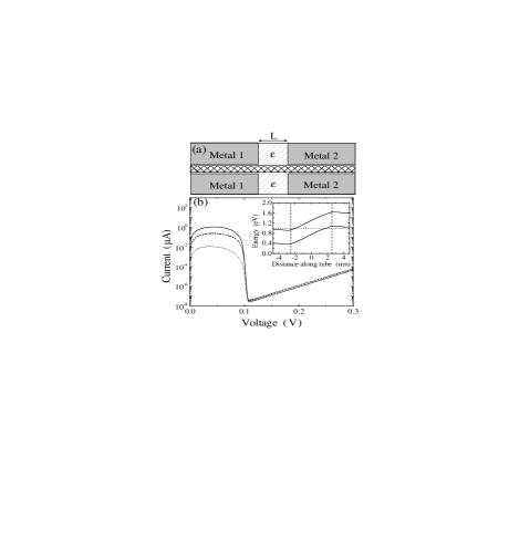
We now consider an NDR device that does not require doping of NTs. As illustrated in Fig. 3(a), the device consists of a semiconducting single-wall NT with each end embedded in a different metal. The metals are spaced apart by a layer of dielectric material.
Conceptually, one can imagine fabricating such a device beginning with a NT growing vertically from a surface [15], and sequentially depositing a metal, a dielectric, and a second metal. The dielectric may be replaced by a metal-oxidation step, and we assume that the materials do not grow on or wet the NT. Possible fabrication processes are discussed further below.
Because the NT does not form covalent bonds with the metal or dielectric, we focus on the limit of weak metal-NT coupling. Then the matrix elements of the NT Hamiltonian are unaffected by the presence of the metal, but charge transfer between metal and NT (and the resulting electrostatic potential) must still be included.
We take the metal on the right to have a workfunction larger than the NT ionization potential, so that electrons are transferred from the NT valence band to this metal. The metal on the left has a workfunction smaller than the NT electron affinity, so that electrons are transferred from this metal to the NT conduction band. Deep within each contact, the population of the NT bands will be determined by equilibrium with that metal, giving an ohmic contact.
The electrodes are modeled as semi-infinite ideal metals. The embedded NT creates a cavity of radius , where represents the van der Waals separation between the NT and the metal. We assume a separation of 0.3 nm, but varying between 0.2 and 0.5 nm has little effect on our results.
For our numerical calculations we again treat a (17,0) NT, self-consistently solving for the potential and charge on the tube at room temperature and calculating the current, as for the p-n junction. The thickness of the dielectric layer separating the electrodes is varied between 2 and 10 nm. The two metal workfunctions are taken to be 1 eV above and below the NT midgap (equivalent to the workfunction of a metallic NT).
The inset in Fig. 3(b) shows the self-consistent band alignment in equilibrium. Because of charge transfer between the metal and NT, the Fermi level is only about 0.1 eV above or below the NT band edge. As for the case of the degenerately doped p-n junction, filled conduction states overlap in energy with empty valence states, permitting tunneling and leading to NDR.
The calculated I-V curves are shown in Fig. 3(b). The peak-to-valley ratio for this device is as high as for the 2 nm device, and even the 10 nm device has a peak-to-valley ratio of . These are orders of magnitude larger than for conventional planar devices [14], and are comparable or better than recently measured ratios in monolayers [16]. Note that the device operation relies on controlling the potential via the electrostatic boundary conditions, with changes of order 1 eV over distances of order the tunneling length. This is possible only because of the nanoscale lateral dimensions, and has no analog in standard NDR devices.
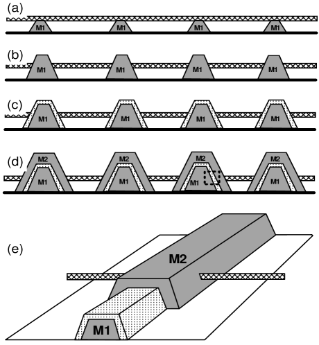
Many strategies are possible for fabrication of the metal-NT-metal device; and a sketch of one is shown in Fig. 4. This is not intended as a realistic proposal for a specific process, but merely to illustrate the issues and opportunities. The process begins by defining parallel lines of the first metal on a substrate, and laying the NT perpendicular to these lines to create a suspended NT structure [Fig. 4(a)]. Then, more of the first metal is deposited on the NT directly over the bottom contacts to create embedded contacts [Fig. 4(b)]. (An alternative method is to suspend the tube on insulating supports and grow the metal lines where the NT is suspended.) To create the dielectric layer, either the surface of the first metal is oxidized [Fig. 4(c)] or a dielectric is deposited as a blanket to cover the whole system. Lines of the second metal are then deposited in alignment with the first metal lines [Fig. 4(d)].
Fabrication of the devices described here poses many practical challenges, but there appear to be no fundamental obstacles in principle. The possibility of integrated fabrication, together with the nanoscale device dimensions, high peak-to-valley ratios, and other desirable properties of NTs, makes these devices attractive candidates for nanoelectronics.
F.L. acknowledges support from the NSERC of Canada.
REFERENCES
- [1] For a recent review, see C. Dekker, Physics Today 5, 22 (1999).
- [2] F. Léonard and J. Tersoff, Phys. Rev. Lett. 83, 5174 (1999).
- [3] A. A. Odintsov, preprint (cond-mat/9910137 v2).
- [4] A. A. Farajian, K. Esfarjani, and Y. Kawazoe, Phys. Rev. Lett. 82, 5084 (1999).
- [5] F. Léonard and J. Tersoff, Phys. Rev. Lett. 84, 4693 (2000).
- [6] D. K. Roy, Tunnelling and Negative Resistance Phenomena in Semiconductors (Pergamon Press, New York, 1977).
- [7] NDR has also been predicted for NTs in fields extending over macroscopic distances, A. S. Maksimenko and G. Ya. Slepyan, Phys. Rev. Lett. 84, 362 (2000). However, because the length scale must be much larger than the elastic mean free path, this effect is not applicable in nanoscale devices.
- [8] K. Esfarjani, A.A. Farajian, and Y. Kawazoe, Appl. Phys. Lett. 74, 79 (1999).
- [9] J. W. G. Wildöer et al., Nature 391, 59 (1998); T. W. Odom et al., Nature 391, 62 (1998).
- [10] Y. Miyamoto et al., Phys. Rev. Lett. 74, 2993 (1995).
- [11] J.-Y. Yi and J. Bernholc, Phys. Rev. B 47, 1708 (1993).
- [12] S. Datta, Electronic transport in mesoscopic systems (Cambridge University Press, Cambridge, 1995).
- [13] M. F. Lin and D. S. Chuu, Phys. Rev. B 56, 4996 (1997).
- [14] S. M. Sze, Physics of semiconductor devices (Wiley-Interscience, New York, 1981).
- [15] J. Li et al., Appl. Phys. Lett. 75, 367 (1999).
- [16] J. Chen et al., Science 286, 1550 (1999).