[
Point defects on III-V semiconductor surfaces
Abstract
The basic properties of point defects (atomic geometry, the position of charge-transfer levels, and formation energies) on the (110) surface of GaAs, GaP, and InP have been calculated employing density-functional theory. Based on these results we discuss the electronic properties of surface defects, defect segregation, and compensation.
Sub. to the Proc. of the XXV ICPS, Osaka (Springer, Berlin/Heidelberg, 2000).
© Springer, Berlin/Heidelberg, 2000.
]
I Introduction
The role of intrinsic point defects in determining the electronic structure of surfaces is a topic that has been debated extensively. They may act as compensation centers and may thus be responsible for Fermi-level pinning at the surface. Consequently, electrically active point defects have been commonly assumed to determine Schottky-barrier heights on metal-covered surfaces [1, 2]. Point defects might also act as nucleation centers for crystal growth and thus influence the surface and interface morphology of devices. Despite the importance of these issues little is known about the basic properties of surface point defects, such as atomic geometry, position of charge-transfer levels, and equilibrium concentration. In the following we will describe how first-principles calculations can be employed to identify the basic properties of surface point defects. Calculations have been performed for GaAs, GaP, and InP. In the present paper we will limit ourselves mainly to GaAs as a model system. Results for vacancies on GaP [3] and InP [4] were published recently.
II Computational Method
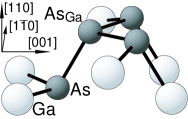
In order to investigate the above noted questions, we performed density-functional theory (DFT) calculations employing the local-density approximation (LDA) for exchange and correlation. Details about the method and extensive convergence tests can be found in Refs. [3, 5]. Surface point defects were calculated with six-layer thick slabs. The (110) surface had a () periodicity in the [] and [] direction, respectively (for the definition of lattice orientations see the coordinate system in Fig. 1a). Test calculations showed that these supercells are large enough to calculate relaxation geometries, electronic structure, and formation energies of point defects accurately [6].
Using the total energy as calculated for the defect and the surface systems we obtain the defect-formation energies as a function of the cation or anion chemical potential and the position of the surface Fermi level [7]. Here we chose the anion chemical potential . To give an example, the formation energy of an arsenic surface vacancy in the charge state , , is:
| (1) |
Here is the total energy of the system with and that of the system without a vacancy. The chemical potential of is controlled by the partial pressure and temperature. It can be varied from gallium-rich () to arsenic-rich conditions () [7], where eV is the heat of formation of GaAs. In Fig. 2, is plotted as a function of . For each point defect and only the charge state with minimum formation energy is shown. According to Eq. (1) the charge state of a defect is given by the slope of the curve. The points where the curve changes it’s slope define the positions of at which the defect changes it’s charge state, i.e. the charge-transfer levels of the defect.
 a)
b)
a)
b)
 c)
d)
c)
d)
 e)
f)
e)
f)
III Atomic and electronic structure of point defects
For several reasons the (110) surface of III-V semiconductors is ideally suited for the study of intrinsic point defects. (i) It is the cleavage plane of these materials and high quality surfaces with a low concentration of steps and defects can be prepared by cleaving wafers. Scanning tunneling microscope (STM) experiments achieving atomic resolution on these surfaces showed point defects such as vacancies and adatoms in a detailed manner [8, 9, 10, 11]. (ii) The surface does not reconstruct but undergoes a relaxation that is characterized by a buckling of surface anions and cations. We calculate the buckling angle to be for GaAs in good agreement with DFT calculations [12] as well as experimental low-energy electron diffraction analysis [13]. The point-group symmetry of the surface is with a single mirror plane pointing in the [] direction. (iii) With the exception of GaP the fundamental band gap of the defect-free surface is free from surface bands. Therefore the presence of point defects with energy levels in the band gap might notably affect the electronic properties of the surface.
A Antisite defects
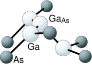
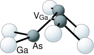
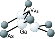
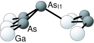
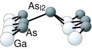
Our calculations show that arsenic antisite defects in the surface layer of GaAs show a rather large displacement of Å in the [] and [] directions (Fig.1a). Thus the defect atom is nearly in the same plane as the surface anions: The large surface buckling between anions and cations of the defect-free surface is locally lifted. The nearest neighbor atoms of and all other atoms in the cell show only small relaxations below Å and Å, respectively. This rather localized relaxation pattern is a typical feature of all surface point defects investigated. The atomic structure of the defect-free surface remains nearly unperturbed beyond second nearest neighbor atoms of surface point defects. As a further common feature of most point defects we find that the symmetry of the surface is well conserved by the defect relaxation. The only exception where we calculate a nonsymmetric relaxation to have a preferable formation energy is the positively charged anion vacancy which will be discussed in subsection III B.
The atomic relaxation of the gallium surface antisite is characterized by a downward and inward movement of the defect with respect to the surface arsenic atoms. The equilibrium position is shifted by Å and Å from the position of the surface anions in the [] and [] direction. The bond length to the neighboring Ga surface atoms is shortened by % compared to the defect-free surface.
Surface antisites on both sublattices do not show any charge-transfer levels inside the band gap. The calculation of the formation energies of the defects reveals that the neutral charge state is always preferable energetically. This is in contrast to antisites in the bulk which we calculate as double acceptors () and double donors () in agreement with previous theoretical studies [14, 15, 16]. We therefore predict that surface antisites will remain charge neutral on intrinsic as well as on - or -type doped material and that they do not alter the electronic properties of the (110) surface. We note that the antisites are electrically inactive at the surface only. Once incorporated into the bulk (e.g. at low temperatures where the surface concentration of defects will be frozen during growth) they become electrically active. This change in character is rather abrupt as we find antisites already in the second layer to be similar to bulk ones in terms of formation energy and electronic structure in agreement with other calculations [17].
B Vacancies
As illustrated in Fig. 1 a vacancy might be derived from an antisite by removing the defect atom. By doing so the atoms surrounding the defect change their equilibrium positions significantly, and we find a very distinct relaxation pattern. The relaxations of the neutral surface vacancies on GaAs are shown in Fig. 1c,d. On both sublattices they are characterized by a comparatively large relaxation of the surface nearest neighbor atoms into the surface by Å () and Å (). The neighboring atom in the second layer also relaxes into the void of the vacancy by Å for both defects. The symmetry of the defect-free surface is conserved by the relaxation of the neutral vacancies. The anion vacancy in the positive charge state, however, prefers a nonsymmetric, rebonded configuration where one of the surface cations approaches the cation in the second layer. The energy gain of this configuration compared to the symmetric relaxation is eV on GaP, eV on InP [4], and eV on GaAs. The latter value as well as the ground-state geometry is in good agreement with the result of eV by Zhang and Zunger [18] for on GaAs.
Based on our calculations we find that surface vacancies are electrically active. They have an amphoteric character on all three materials investigated, i.e., they are positively charged on - and negatively charged on -type material. on GaAs has two charge-transfer levels and in the lower half of the band gap while is a negative U center with in the lower half of the band gap as shown in Fig. 2. We can therefore conclude that vacancies are efficient compensation centers for - and -type conditions.
C Adatoms
As a last type of surface point defects we have calculated anion adatoms. As illustrated in Fig. 1 we find two possible configurations: one in which the adatom is bonded to the surface anions (, Fig. 1a) and one with bonds to the surface cations (, Fig. 1b). In the configuration the distance between the adatom and the arsenic surface atoms is Å in the neutral charge state while for the distance to the surface gallium atoms is Å. The adatom is located Å () and Å () above the surface. The defect bound to surface arsenic has an electronic structure similar to the surface vacancies showing two charge-transfer levels and (Fig. 2). In contrast, , which bonds to the surface cations, is predicted to be negatively charged for all positions of the Fermi level except for extreme -type conditions with below eV, where the neutral charge state is found to be stable.
Unlike previous first-principles calculations by Yi et al. [19] the adatom is determined as the preferred adsorption site over a wide range of the surface Fermi level (Fig. 2). Only for -type conditions near the valence-band maximum in the singly positive charge state has a lower formation energy than . For the neutral charge states the difference in formation energy is eV while Yi et al. [19] report a difference of eV. This difference might be due to the limited size of the surface unit cell () and the use of the point only for Brillouin zone integration as employed in Ref. [19].

a)

b)
IV Formation energies and defect concentrations
Based on the formation energies as shown in Fig. 2 we identify the dominant point defects on the surface and how the concentration depends on the anion chemical potential and doping conditions. Under gallium-rich conditions the gallium antisite is lowest in formation energy (Fig. 2a). It is, however, not electrically active and thus can be excluded as a possible dopant or compensation center. The dominant point defect on GaAs under gallium-rich conditions is the arsenic vacancy , positively charged under -type and negatively charged under -type conditions. This conclusion changes if we consider arsenic-rich and -type conditions. Then and , both in the singly positive charge state, are almost degenerate in formation energy (Fig. 2b). With in the upper half of the band gap the negatively charged is the defect with the lowest formation energy among all electrically active point defects. Fig. 2b also shows that the neutral has a negative formation energy under arsenic-rich conditions. This indicates that the surface is unstable against the formation of a complete layer of arsenic. Indeed, first-principles calculations of the surface energy show this structure to be lower in energy than the cleavage surface assuming extreme arsenic-rich conditions [20].
Based on the calculated formation energies we can immediately obtain the equilibrium concentration of point defects. Neglecting vibrational entropy contributions this quantity is determined by the number of possible sites where a defect can be formed, the formation energy , and temperature :
| (2) |
Here is Boltzmann’s constant. Using this formalism, assuming room temperature, and taking into account the electrically active defect with the lowest ( eV for under gallium-rich conditions with at the conduction-band minimum) we find a maximum equilibrium concentration of about . The concentration decreases if we assume a situation where the Fermi level is fully pinned at the charge-transfer level of the vacancy at eV above the valence-band maximum. Then the formation energy becomes eV and the concentration is negligible (). A simple analysis shows that pinning of the surface Fermi level by defects requires rather large concentrations of about [21]. This conclusion is consistent with combined STM and photoelectron spectroscopy measurements on InP(110), which showed significant surface band bending at concentrations of phosphorus surface vacancies higher than [4]. However, also for the phosphorus surface vacancy we find an equilibrium concentration (at K where the experiment has been performed) significantly below the experimentally observed defect concentration. We therefore conclude that the formation of vacancies is driven by kinetic mechanisms rather than as a result of thermal equilibrium. A possible kinetic processes on the surface is diffusion from the bulk driven by the lower formation energy of surface vacancies compared to their bulk counterparts.
V Summary and conclusions
Density-functional theory has been used to study point defects on the (110) surface of GaAs. We identify antisites on both sublattices to be the defects with the lowest formation energy. They are not electrically active and can therefore be excluded as compensation centers on this surface. Among the electrically active point defects is lowest in formation energy under gallium-rich conditions. For arsenic-rich conditions and -type doping and arsenic adatoms are predicted to be most important. The calculated formation energies allow the estimation of the equilibrium concentrations of surface defects. We have shown that the formation energy of all electrically active defects is too high to allow for equilibrium concentrations large enough to induce significant band bending at the surface. The high concentration of defects reported in recent experiments is thus related to kinetic effects.
This work was supported by the ‘Deutsche Forschungsgemeinschaft’ through ‘Sonderforschungsbereich’ 296 TP A5. We like to thank Ph. Ebert and K. Horn for stimulating discussions.
REFERENCES
- [1] W. E. Spicer et al., J. Vac. Sci. Technol. B 6, (1988) 1245.
- [2] W. Mönch, Surf. Sci. 299/300, (1994) 928.
- [3] G. Schwarz, A. Kley, J. Neugebauer, and M. Scheffler, Phys. Rev. B 58, (1998) 1392.
- [4] P. Ebert et al., Phys. Rev. Lett. 84, (2000) 5816.
- [5] M. Bockstedte, A. Kley, J. Neugebauer, and M. Scheffler, Comp. Phys. Commun. 107, (1997) 187, see also: http://www.fhi-berlin.mpg.de/th/fhimd/.
- [6] Gallium surface vacancies on GaAs (110) change formation energies and the position of Kohn-Sham eigenstates in the band gap by less than 10 meV when increasing the supercell to () or () periodicity. Relaxation pattern coincide in these calculations better than by Å.
- [7] U. Scherz and M. Scheffler, in Imperfections in III-V Materials, semiconductors and semimetals, edited by E. R. Weber (Academic Press, New York, 1993), Vol. 38, Chap. 1, p. 1.
- [8] G. Cox et al., Vacuum 41, (1990) 591.
- [9] S. Gwo, A. R. Smith, and C. K. Shih, J. Vac. Sci. Technol. A 11, (1993) 1644.
- [10] G. Lengel, R. Wilkins, and M. Weimer, Phys. Rev. Lett. 72, (1994) 836.
- [11] P. Ebert, K. Urban, and M. G. Lagally, Phys. Rev. Lett. 72, (1994) 840.
- [12] J. L. A. Alves, J. Hebenstreit, and M. Scheffler, Phys. Rev. B 44, (1991) 6188.
- [13] C. B. Duke, C. Mailhiot, and A. Paton, J. Vac. Sci. Technol. B 3, (1985) 1087.
- [14] G. A. Baraff and M. Schlüter, Phys. Rev. Lett. 55, (1985) 1327.
- [15] J. Da̧browski and M. Scheffler, Phys. Rev. Lett. 60, (1988) 2183.
- [16] S. B. Zhang and J. E. Northrup, Phys. Rev. Lett. 67, (1991) 2339.
- [17] R. B. Capaz, K. Cho, and J. D. Joannopoulos, Phys. Rev. Lett. 75, (1995) 1811.
- [18] S. B. Zhang and A. Zunger, Phys. Rev. Lett. 77, (1996) 119.
- [19] J.-Y. Yi et al., Phys. Rev. B 52, (1995) 10733.
- [20] N. Moll, A. Kley, E. Pehlke, and M. Scheffler, Phys. Rev. B 54, (1996) 8844.
- [21] W. Mönch, Semiconductor Surfaces and Interfaces, Springer Series in Surface Sciences Vol. 26, edited by G. Ertl. et al. (Springer, Berlin/Heidelberg, 1993).