Institut für Theoretische Festkörperphysik, Universität Karlsruhe, 76128 Karlsruhe, Germany
Forschungszentrum Karlsruhe, Institut für Nanotechnologie, 76021 Karlsruhe, Germany
Coulomb blockade, tunnelling Scattering mechanisms and Kondo effect
Orbital and spin Kondo effects in a double quantum dot
Abstract
Motivated by recent experiments, in which the Kondo effect has been observed for the first time in a double quantum-dot structure, we study electron transport through a system consisting of two ultrasmall, capacitively-coupled dots with large level spacing and charging energy. Due to strong interdot Coulomb correlations, the Kondo effect has two possible sources, the spin and orbital degeneracies, and it is maximized when both occur simultaneously. The large number of tunable parameters allows a range of manipulations of the Kondo physics – in particular, the Kondo effect in each dot is sensitive to changes in the state of the other dot. For a thorough account of the system dynamics, the linear and nonlinear conductance is calculated in perturbative and non-perturbative approaches. In addition, the temperature dependence of the resonant peak heights is evaluated in the framework of a renormalization group analysis.
pacs:
73.23.Hkpacs:
72.15.QmIntroduction. Recently there has been substantial interest in many-body and correlation effects in ultrasmall semiconductor quantum dots. The dots may have strong electron-electron interactions, characterized by the charging energy , and large level spacing (typically ) [1]. At low temperature and strong coupling between the dot and the leads, , quantum fluctuations of the charge and spin degrees of freedom strongly affect the transport through the dot [2, 3, 4, 5, 6]. The spin fluctuations lead to the Kondo effect, which has been verified in experiments on single quantum dots[7].
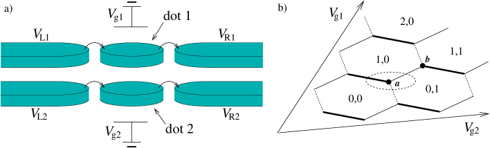
The Kondo effect has recently been discovered also in a double quantum-dot structure [8]. Motivated by these experiments, we consider in the present work a system of two capacitively-coupled quantum dots, depicted in Fig. 1a). The level spacings in each dot are large, and effectively just one level per dot is coupled to the two reservoirs. For strong tunnel coupling and spin-degenerate levels, each dot would separately display the usual spin-Kondo effect in its characteristics. In the present case, the interdot interaction is assumed strong rendering the charge states and of the two dots strongly correlated. Consequently, the Kondo effect of each dot is sensitive to and can be manipulated by voltages applied to the other dot. The strong interdot interaction has also another, more dramatic effect: the Kondo effect can arise from the orbital degeneracy (the two dot levels tuned to resonance) even in absence of the real spin degree of freedom[8]. The present model, with two spin-degenerate levels, allows us to study the interplay of the two Kondo effects as a function of different voltages as well as the level splitting. In absence of orbital degeneracy, the differential conductance can exhibit satellite resonances for finite bias voltages ; these may be easier to observe than split peaks in the case of single dots (e.g. due to Zeeman splitting [3, 4] or a second level in the dot [5]).
The paper is organized as follows. First the model for the double-dot system is introduced. Then we express the current and conductance in terms of the spectral density of the dot states in the framework of a real-time diagrammatic technique. We calculate the linear and nonlinear conductance through each dot as a function of the two transport and the two gate voltages. This calculation is complemented by a poor man’s scaling analysis of the temperature dependence of the linear conductance.
The model. The double-dot system shown in Fig. 1a) is governed by the Hamiltonian , where describes non-interacting electrons in the reservoir ( and ), refers to the dot electrons, and is the tunnelling Hamiltonian. For each barrier we introduce the tunnelling strength , which is assumed to be independent of energy in the range of interest ( is the density of states in the leads). The electron-electron interaction, for electrons in the dot , is accounted for by the charging energy . In general, the interaction depends on all the voltages applied to the system, but for symmetrically applied transport voltages it is determined by the gate voltages and alone.
In the plane spanned by these gate voltages, within the hexagonal areas depicted in Fig. 1b), the ground state is reached for the charge configurations indicated in the figure, and electron tunnelling is suppressed by Coulomb blockade effects. In the figure, there are three kinds of boundaries in the honeycomb lattice. Electron transport through dot 1 (2) is only possible along the boundaries indicated with the thick (dashed) lines, while the thin lines correspond to degeneracy between the two dots, in particular, along the - line. As in the experiment, where the two dots lie close on top of each other, both the intradot and interdot interactions are assumed to be strong. Hence, for low temperature and bias voltages, , it suffices to consider three charge states. Below we focus on the circled region in Fig. 1b), i.e. the states (0,0), (0,1), and (1,0). In this restricted basis, the states can be newly defined to include the charging energy , e.g., for an electron with spin in dot , . We observe that the resulting Hamiltonian has a one-to-one correspondence to a single-dot model with two (spin-degenerate) orbital states, distinguished by an orbital quantum number . The index corresponds to the spatially separated dots and is therefore conserved in the tunnelling processes.
Transport. We aim to evaluate the differential conductance () from the current through the dot . The dc-current can be expressed as [3]
| (1) |
Here are the Fermi functions of the leads with chemical potentials . The spectral density of the state corresponds to a local density of states in the quantum dot(s). Its shape is reflected in the differential conductance.
In the weak-coupling limit, the lowest-order perturbation theory yields which describes the suppression of the current, i.e., Coulomb blockade effects. In second order, or ‘cotunnelling’ regime, the spectral density takes the form
| (2) | |||
where are the occupation probabilities for the states as obtained in the lowest-order perturbation theory [12] and . As the prefactor in Eq. (2) suggests, only decays algebraically as leading to a non-vanishing conductance everywhere in the plane in Fig. 1b). The resulting linear conductance – denoted as in the following – as a function of shows a maximum for , i.e., on the line - in Fig. 1b) (this straight-forward result is not displayed). As a function of the transport voltage , for symmetric applied voltages for both , the differential conductance exhibits smooth variations, which are displayed as the two lowest curves in Fig. 2a).
For stronger coupling, further higher-order processes become important. We account for them within the so-called resonant-tunnelling approximation [4], which amounts to a resummation of a certain class of diagrams (with maximally two-fold off-diagonal density matrix) in all orders in the tunnelling amplitudes. To gain some insight into the results, let us consider again the symmetric applied voltages, equal barriers, , and degenerate levels (i.e. the - line in Fig. 1b)). In this case, all the spectral densities are equal, , and can be calculated explicitly:
| (3) |
Here denotes the degeneracy of the resonance and the level renormalization . For a single level without spin, , only charge fluctuations are possible and Eq. (3) reduces to the Breit-Wigner formula with an unrenormalized Lorentzian form. For two spinless levels, , and the orbital index behaves like a pseudospin; for two spin-degenerate levels we have . If , the (pseudo)spin dynamics contributes to Eq. (3) and, at low temperature and for small excitation energies, it dominates over the charge fluctuations. As a consequence an additional sharp resonance, the Kondo peak, emerges in at the positions of the chemical potentials in the leads. Figure 2b) shows an example of for and introduces a schematic way for visualizing its relevant structure. The Kondo peak is reflected in the conductance as a sharp zero-bias maximum, dot-dashed curve in Fig. 2a), which is a distinctive sign of the Kondo effect. The peak in is the higher the larger is, in accordance with the -dependent Kondo temperature, see below.
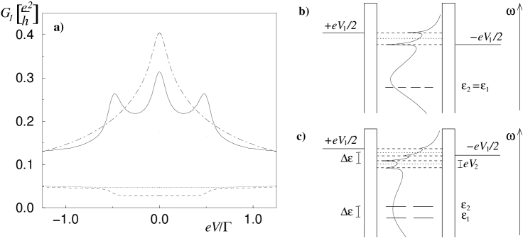
The most intriguing results are found for the general case with non-degenerate levels ( for detuned dots, and/or in a magnetic field) and/or different bias voltages, . In order to account for these extensions, we calculate numerically. For brevity of the following discussion, we set the magnetic field to zero and focus on the conductance through dot 1. Figure 2a) (solid line) shows an example of for equal bias voltages, , and a finite level separation . The conductance reflects the shape of the spectral function , illustrated in Fig. 2c), which exhibits resonances at and . The former arise due to the spin fluctuations in dot 1 and are similar to the usual Kondo peaks; the latter are due to tunnelling processes involving both levels – i.e. fluctuations of the orbital index – and thus depend on the level separation . As a rule, the conductance shows a peak whenever two of the resonances in coincide: there is a zero-bias maximum due to the spin-degeneracy of the levels (although the levels are now detuned) and, in addition, two satellites at – these correspond to the additional peaks in and reflect the presence of the other level/dot.
An experimental observation of the satellites in is facilitated by two points. First, finite bias voltages induce decoherence to the electron transport and tend to suppress the Kondo effect for too high voltages [9]. However, in the present case the splitting can be controlled starting from zero and only small bias voltages are required in observing the splitting. Second, due to the larger number of states (=4) the split peaks are more pronounced in the present system than, e.g., for a single dot with one Zeeman-split level (altough they have been observed [7] in this case as well).
The fact that the voltages can be chosen independently opens new interesting possibilities. Let us consider the spectral density in Fig. 2b) and the splitting of the Kondo resonance by the applied bias voltage. In the case of single quantum dots, the voltage-induced split in is reflected as a mere monotonous decrease of the differential conductance . In the present system, however, the linear conductance is found to show a peaked structure as a function of the voltages and () applied to the other dot, see Fig. 3a). The peaks in occur when the condition is fulfilled, see Fig. 2c) and above.
Before embarking on the scaling analysis, let us make a remark concerning the “Kondo regime”: it turns out that may display a peaked structure also outside this regime. Let us consider a higher temperature than above, e.g. , and tune the system into the mixed-valence regime with the levels brought into a close vicinity of the Fermi energies in the leads. In this case, no Kondo effect is expected. A perturbative calculation produces the usual Coulomb blockade peaks, which in this case are four peaks that shift with ; the non-perturbative result for shown in Fig. 3b) displays a triple-peak structure with one peak at zero-bias and two satellites at . The number and position of these peaks suggest that the peaks in could be due to the Kondo effect after all, cf. results obtained above. On the other hand, if the peaks were of the Kondo origin, their width should reflect (or , the inverse decoherence time of Ref. [9], should this exceed the temperature), where is the new low-energy scale, the Kondo temperature. However, in Fig. 3b) the resonance widths are seen to be almost , see the energy scales indicated in the figure; see also Ref. [11]. Hence, although the peak widths are not a strict measure of the Kondo regime, we conclude that higher-order tunnelling processes may also give rise to non-trivial peaked structure other than the Kondo type.

Scaling. In this section, we complement the above considerations in the framework of the poor man’s scaling technique [14], a renormalization group approach suited for the Kondo regime at equilibrium (zero-bias limit). This approach is used to derive explicit expressions for the logarithmic temperature dependence of the linear conductance – experimentally the most convincing sign of the Kondo effect – and the Kondo temperature .
In order to obtain the proper scaling form of the conductance, we consider the dots deep in the Coulomb blockade regime, , and start by Schrieffer-Wolff (SW) transforming the Hamiltonian into the scattering form
| (4) | |||||
| (5) |
For degenerate states, , corresponds to the Coqblin-Schrieffer model[14]. The current through both dots, , calculated in the lowest (second) order in is
| (6) |
where are the same probabilities that entered Eq. (2) and
| (7) |
are the tunnelling rates from reservoir to [15]. Here is assumed, implying . It should be noted that despite its different appearance, the present formulation yields just the cotunnelling current expressed above in terms of Eqs. (1) and (2). However, Eqs. (6) and (7) are more suitable for the scaling analysis to follow.
In the next step towards , we perform poor man’s scaling to second order in the coupling constants. In the degenerate case, , there is just one coupling constant in the problem and it is renormalized as [16]. The initial high-energy cutoff corresponds to the band width in the leads, while the final cutoff is taken as (or , the decoherence rate of Ref. [9]). The second equality for follows from the definition of the Kondo temperature . This in turn yields an increasing for increasing and gives a qualitative reason, why the zero-bias peak in is emphasized for larger values of , see above.
Assuming that the zero-bias limit can be modelled in terms of equilibrium properties of the system, we insert the scaled coupling constants into Eq. (6) and obtain
| (8) |
for the leading cutoff dependence of the peak conductance. The conductance through just one dot is sensitive to the voltage : If , , while for , is obtained from Eq. (8) by replacing the -dependent part by .
Summary. In conclusion, we have studied electron transport through a capacitively-coupled double quantum dot with a large level spacing and intra and interdot charging energies. The system is found to exhibit the Kondo effect due to fluctuations in both the orbital and spin degrees of freedom. The linear and nonlinear conductance is calculated for arbitrary level positions and bias voltages and it is found to display a rich structure both in and out of the Kondo regime. For detuned levels, the differential conductance displays zero-bias as well as satellite peaks. The side peaks are argued to be experimentally observable despite the suppressive effect of finite bias voltages [9]. The Kondo effect in each dot is shown to be very sensitive to the voltages applied to the other dot allowing delicate manipulation of the Kondo physics. An example of voltage-induced splitting of the Kondo peak has been discussed.
Acknowledgements.
We would like to acknowledge J. Schmid, J. Weis, and U. Wilhelm for discussions. This work has been supported by the Finnish Cultural Foundation, EU TMR network “Dynamics of Nanostructures”, the Swiss National Foundation, and DFG through SFB 195.References
- [1] H. Schoeller, in Mesoscopic Electron Transport, NATO ASI, Series E, Vol. 345, Kluwer (1997), and references therein.
- [2] T.K. Ng and P.S. Lee, Phys. Rev. Lett., 61 (1988) 1768; L.I. Glazman and M.E. Raikh, JETP Letters, 47 (1988) 452.
- [3] Y. Meir, N.S. Wingreen and P.A. Lee, Phys. Rev. Lett., 70 (1993) 2601.
- [4] J. König, H. Schoeller and G. Schön, Phys. Rev. Lett., 76 (1996) 1715; J. König et al., Phys. Rev. B, 54 (1996) 16820.
- [5] T. Pohjola et al., Europhys. Lett., 40 (1997) 189; J. Low Temp. Phys., 118 (2000) 391.
- [6] W. Izumida, O. Sakai and Y. Shimizu, J. Phys. Soc. Jpn., 67 (1998) 2444; A.L. Yeyati, F. Flores and A. Martin-Rodero, Phys. Rev. Lett., 83 (1999) 600; M. Pustilnik, Y. Avishai and K. Kikoin, Phys. Rev. Lett., 84 (2000) 1756.
- [7] D. Goldhaber-Gordon et al., Nature (London), 391 (1998) 156; S.M. Cronenwett, T.H. Oosterkamp and L. Kouwenhoven, Science, 281 (1998) 540.
- [8] U. Wilhelm and J. Weis, Physica E, 6 (2000) 668; unpublished.
- [9] A. Kaminski, Yu.V. Nazarov and L.I. Glazman, Phys. Rev. Lett., 83 (1999) 384.
- [10] J.M. Elzerman et al., J. Low Temp. Phys., 118 (2000) 375.
- [11] H. Schoeller and J. König, Phys. Rev. Lett., 84 (2000) 3686.
- [12] These probabilities can be obtained, e.g., by using detailed-balance relations.
- [13] The peak is maximized for a finite level splitting, , due to the increase in the occupation probability of dot 1 and the subsequent increase in the weight under .
- [14] A.C. Hewson, The Kondo Problem to Heavy Fermions, Cambridge University Press, 1993.
- [15] The functional form of these rates is similar to that for a single tunnelling barrier between two metal leads, emphasizing the idea of fluctuations extending through the dot.
- [16] In the non-degenerate case, , the scaling equations would need to be solved numerically. This is also the case close to the point of Fig. 1b); there the coupling constants are found to scale, but in a different way.