Ballistic reflection at a side-gate in a superconductor-semiconductor-superconductor structure
Abstract
We have fabricated a sub-micron-sized structure consisting of an InAs-based 2DEG, two narrow Nb leads and a gate, where the indirect ballistic transport between the non-oppositely superconducting contacts can be controlled by the voltage applied to the gate. This new kind of tuneable junction can be used for applications and allows several fundamental questions related to the transport mechanism to be studied. First results of experiments carried out in this respect are presented.
pacs[74.40+k,74.50.+r]
1 Introduction
Controllable Josephson weak links using semiconducting material as a barrier were used to investigate fundamental transport mechanisms as well as possible applications. By influencing the carriers inside the semiconductor, Josephson field effect transistors [1], non-equilibrium junctions [2, 3, 4] or optically modulated weak links [5, 6] were demonstrated. In this article we present a novel device, where the transport of ballistic carriers can be controlled by a tunable side-gate.
Only recently, more realistic descriptions have been provided of devices where superconductors are attached to a 2DEG and all dimensions are comparable to the phase-breaking length [7]: as depicted in Fig.1a, taking into account a realistic geometry with two dimensions in which carriers can transfer from one superconducting contact to the other, a modified subgap structure [7], different density of states [8] and a different magnetic field dependence are theoretically predicted consequences of these non-local modes.

In Josephson junctions, the existence of these modes is related to the angular dependence of the Andreev reflection probability and can play a crucial role: whenever the roughness of the interface between the superconductor and the barrier material is larger than the Fermi wavelength of the quasiparticles inside the normal conducting region, the transport is in fact neither perpendicular nor restricted to one dimension any more, as shown in Fig.1b.
The angle dependent reflection probability at perfect interfaces between two materials depends on the ratios of their carrier densities and on their effective masses or, correspondingly, on their Fermi velocities and wave vectors . At a non-idealized superconductor-semiconductor interface the total barrier strength can be described by an effective angle dependent parameter [7], which allows the iv-characteristic of a Josephson junction to be calculated more accurately using a generalized OBTK model. However, the underlying angular dependence has neither been verified experimentally nor used for application.
2 Samples
In structures with gates previously studied, the carrier density in the semiconducting barrier was modulated homogeneously and locally [9], or small channels were defined through which the superconductors are coupled [10]. In contrast to this, in the case of our devices a potential barrier can be introduced at a certain position within the 2DEG depending on the voltage applied to the gate. At this position ballistic reflection of the carriers occurs [11]. Quasiparticles which are injected into the 2DEG from one superconductor can reach the other superconductor only indirectly by undergoing normal reflection at this induced potential barrier. An AFM picture of a fabricated structure with which this effect can be demonstrated is shown in Fig.2. Local shifting the potential barrier by a change of defines both, the angle at which the other superconductor can be reached and the effective length of the path.
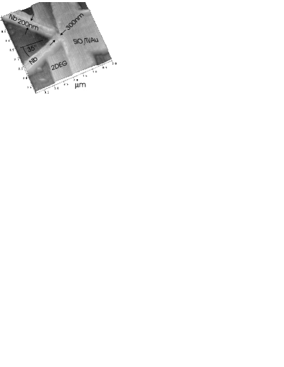
The structure has been fabricated by dry and selective wet etching of an InAs/AlSb/GaSb heterostructure. The Nb leads were evaporated on top of the InAs layer after weak Ar plasma cleaning. To avoid gate leakage, an evaporated layer of Ti/Au was electrically isolated by a SiOx layer. Several sets of samples with different angles and dimensions were prepared using 2DEGs with a carrier concentration of and mobility of . This results in mean free paths of 3.15 , which is much larger than the device’s dimensions so that the transport is far in the ballistic regime. The alignment of side-gate, Nb-leads and etching masks with respect to each other turned out to be the most delicate part.
3 Results
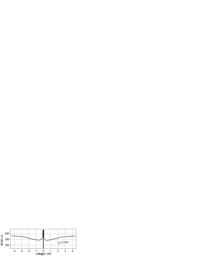
We measured the iv-characteristics and the differential resistance of the device by a standard four-point technique between the two Nb leads and determined its dependence on . As can be deduced from the curve in Fig.3, where a sharp dip at zero bias voltage and an excess current can be seen, a superconductive coupling is formed [12].
In Fig.4 the normal resistance of the device is plotted against . Above a certain positive voltage the resistance reaches a constant maximum value. This corresponds to the situation, where there is no induced potential barrier and ballistic electrons are not reflected. The indirect transport from one Nb-lead to the other is therefore very improbable [13]. The occurrence of this offset in has been reported several times [14] and is about in our case. As is reduced the normal resistance decreases and reaches its minimum value at about V. The indirect transport via reflection at an induced potential barrier decreases the resistance and emerges an optimum when the corresponding path has the highest Andreev reflection probability. A further reduction of slowly increases the normal resistance again, as the angle of incidence of injected quasiparticles becomes less favorable.
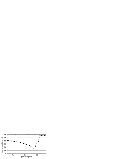
Thus the side-gate can be used to adjust the focus of the transport of ballistic quasiparticles, which enables a large change of the normal resistance. Best coupling could be achieved at an effective gate voltage of -0.15 V and a resulting theoretical maximum potential barrier height of 150 meV [15], which is reasonable compared with the Fermi energy of the 2DEG of meV. A quantitative model for the effect observed must take the precise profile of the induced potential, its rise and shift depending on , and the resulting possible transport modes inside the device into consideration [16].
4 Summary
In summary, we fabricated a new type of tunable ballistic Josephson junction with the unique possibility of changing the effective electrode separation. In addition, the angular dependence of Andreev reflection and the formation of non-local modes can be made use of and studied with this device. A modulation of the normal resistance by up to 500% could be achieved.
References
- [1] T.D. Clark, R.J. Prance, and A.D.C. Grassie, J. Appl. Phys. 51, 2736 (1980).
- [2] L.R. Testardi, Phys. Rev. B 4, 2189 (1971).
- [3] A.F. Morpurgo, T.M. Klapwijk, and B.J. van Wees, Appl. Phys. Lett. 72, 966 (1998).
- [4] J.A.A. Baselmans, A.F. Morpurgo, B.J. van Wees, and T.M. Klapwijk, Nature 397, 43 (1999).
- [5] G. Bastian, E.O. Göbel, J. Schmitz, M. Walther, and J. Wagner, Appl. Phys. Lett. 75, 94 (1999).
- [6] T. Schäpers, R.P. Müller, A. Kaluza, H. Hartdegen, and H. Lüth Appl. Phys. Lett. 75, 391 (1999).
- [7] N.A. Mortensen, K. Flensberg, and A.-P. Jauho, Phys. Rev. B 59, 10176 (1999), cond-mat/9807049.
- [8] S. Chaudhuri, and P.F. Bagwell, Phys. Rev. B 51, 16936 (1995).
- [9] H. Takayanagi, V.N. Antonov, E. Toyoda, J. Korean Phys. Soc. 34, S148 (1999).
- [10] H. Takayanagi, T. Akazaki, and J. Nitta, Phys. Rev. Lett. 75, 3533 (1995).
- [11] This side-gate technique was successfully used previously to shift the effective boundary for transport through a quantum Hall sample: Y.Y. Wei, J. Weis, K. von Klitzing, and K. Eberl, Phys. Rev. Lett. 81, 1674 (1998).
- [12] The exact value of the critical current could not be measured due to rounding caused by different sources of noise.
- [13] In a real sample, a residual coupling between the superconductors occurs for all gate voltages. Quasiparticles can be back-scattered or pass through a small part that unintentionally connects the Nb-contacts directly. In addition, an induced attractive electron-electron interaction can explain this behaviour: G. Bastian et al. Comment on ”Critical currents in ballistic two-dimensional InAs-based superconducting weak links”, submitted to Phys. Rev. B (1999).
- [14] A. Kristensen, J. Bo Jensen, M. Zaffalon, C.B. Sørensen, S. M. Reimann, M. Michel, A. Forchel J. Appl. Phys. 83, 607 (1998).
- [15] L.I. Glazman, and I.A. Larkin, Semicond. Sci. Technol. 6, 32 (1991).
- [16] N.A. Mortensen, and G. Bastian, submitted to Superlattices and Microstructures (2000), cond-mat/0005404.