An anomalous alloy:
Abstract
We study via density functional-based molecular dynamics the structural and dynamical properties of the rare earth silicon amorphous alloy for and . The network forms cavities in which a cation is entrapped. Its electrons are transferred to the network and are located in the dangling bonds of the atoms that line the cavities. This leads to the presence of low coordinated atoms that can be described as monovalent or divalent anions. For , the cavities touch each other and share atoms that have two dangling bonds. The vibrational spectrum is similar to that of amorphous . However, doping induces a shoulder at 70 cm-1 and a pronounced peak at 180 cm-1 due to low coordinated .
Rare earth doped silicon alloys have received considerable attention due to their intriguing properties and for their potential in the applied domain. They show an interesting metal-insulator transition and their optical conductivity exhibits apparent sum rule violations [1], as in manganates and high compounds. In addition alloys have an enormous negative magneto resistance [2] and spin-glass behaviour has been reported [3]. In spite of a large number of experimental investigations the structure of this and related compounds is still a matter of guesswork. For this reason we have undertaken here an ab-initio molecular dynamics investigation of the alloy. This is non-magnetic but has electronic structure properties that set it apart from all the other amorphous alloys so far studied.
In our simulation we followed the method of Car and Parrinello [4] as implemented in the CPMD code [5]. Local density approximation and norm-conserving Goedecker-type pseudopotentials have been used [6], [7] (for the semi-core 4d states have been included in the valence). The simulation cell is a cube of length 11.216 Å containing a total of 64 atoms. Periodic boundary conditions are applied. The concentrations () and () have been studied. The Car-Parrinello equations of motion with a fictitious electronic mass of 400 a.u. were integrated using a time step of 3 a.u. (0.072 fs). In order to generate the amorphous structure we used the following procedure. We start from a cubic lattice with the atoms placed randomly, but as far as possible from one another. Such an unlikely configuration is rapidly destroyed and leads to fast melting. The system is kept in this liquid state at the temperature of 1650 K for about 0.35 ps, in order to lose memory of the initial condition. Then the temperature is brought down to 300 K in a time span of 0.3 ps.
Although the annealing rate is rather fast, past experience in semiconducting alloys has shown that the main features of the amorphous structure are well reproduced [8] . The system was finally allowed to evolve at 300 K for 10 ps without ionic temperature control. The system is a metal in the liquid state and a small gap semiconductor when amorphous at room temperature. In the annealing part of the run we controlled the fictitious electronic kinetic energy drift by periodic quenches to the Born Oppenheimer surfaces. Instead a Nose’ thermostat was used for the electrons in the last 10 ps. The thermostat characteristic frequency was 1500 cm-1 and the target electronic fictitious kinetic energy was set according to the prescription of reference [9]. The vibrational spectrum and other statistical averages were evaluated during the last 10 ps.
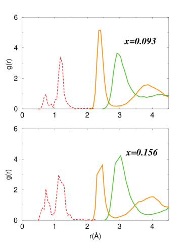
In Fig. 1 we report the measured correlation functions and . Due to the small number of atoms the ’s are very noisy and are not reported in order not to clutter the figure. However they show a strong tendency for the to repel each other. From the correlation functions as well as a visual inspection of the structure we could infer that atoms tend to form a tetrahedrally bonded amorphous network as in pure . However atoms are not part of the amorphous network but sit at the centre of cavities. In order to accommodate these cavities the network has to generate a number of under-coordinated atoms in the proximity of the impurities.
A very valuable help in understanding the electronic properties of amorphous structures is provided by the maximally localised Wannier functions [10] and their centres, as discussed in ref. [11] for the case of pure . Wannier functions are obtained from the Kohn and Sham orbitals by performing a unitary transformation that minimises the average orbital spread. The resulting orbitals capture the chemical nature of the bond. An even simpler and more vivid picture is obtained by considering only their centroids.
This is demonstrated in Fig. 1 where we plot the Wannier centre correlation functions. The fist peak is split into two. The higher peak is centred at half of the bond distance and clearly reflects the formation of the covalent bond. There is, however, a very sizable peak at shorter distances which is due to the presence of dangling bonds, whose height increases with concentration. Since these peaks are well separated we can classify the Wannier centre and the corresponding Wannier functions into “covalent” and “dangling”. The different nature of these classes of functions is reflected also in their spread distribution, which is bimodal with peaks centred at 1.5 Å and 1.85 Å for “covalent” and “dangling” bonds respectively.
As in ref. [11] we can identify the covalently bonded atoms as those pairs of atoms which share “covalent” Wannier functions. Using this criterion, which is based on the chemistry of the system and not simply on a geometric distance consideration, we find that in the network there are twofold, threefold and fourfold-coordinated atoms. As a function of the concentration, due to the need to accommodate more impurities, the number of threefold-coordinated silicons increases noticeably (from to ) while that of fourfold-coordinated atoms decreases (from to ). We also noticed an increase of the twofold-coordinated silicons; however, due to the limited statistics we do not attempt to define here the probability of their occurrence.
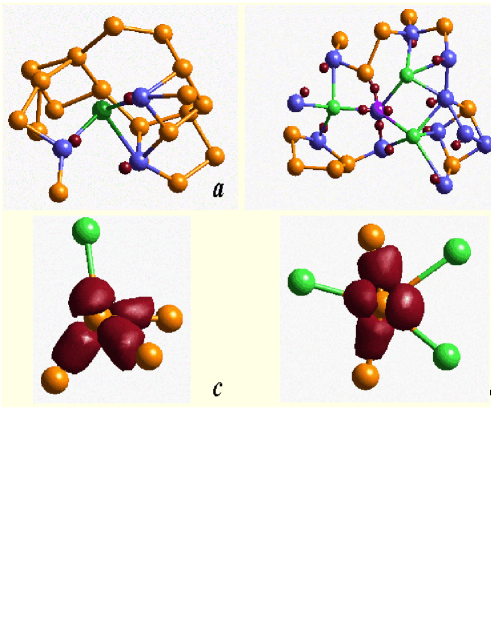
In Fig. 2 we show two typical environments for the atoms. At the higher concentration the atoms have to share some of their first neighbours. These shared atoms tend to be twofold coordinated as shown in the picture. Finally the Wannier analysis shows clearly that has lost all its valence electrons and is in the oxidation state 3+ . Thus the picture that emerges from our simulation is one in which the atoms donate their valence electrons to the sub-lattice. These electrons are then stored in the network and localised in the doubly occupied dangling bonds of the threefold and twofold coordinated atoms. These atoms are therefore negatively charged and can be thought of as being a realization of the species and . These species tend to cluster around the cation, not only to form the cavity in which the impurity sits but also to ensure local charge neutrality. As such they are an integral part of the structure. The silicon dangling bonds provide the ligand field to the metal ion.
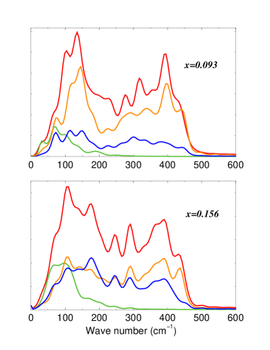
In Fig. 3 we show the vibrational density of states analysed in the contributions from the species , and . The general appearance of the spectrum is very similar to that of pure . However, we note a shoulder 70 cm-1 which is due to the atoms; we also note that, especially for , the make an important contribution and together with the alter the relative intensities of the peaks. Since is expected to have a higher infra-red activity than we can predict that the infra-red spectrum will show an enhancement of the 180 cm-1 peak, and a related structure at 70 cm-1. The intensities of either peak should increase as a function of .
For a selected small number of configurations we evaluated the HOMO-LUMO gap. This shows large oscillations in the range 0.2 to 0.45 eV.
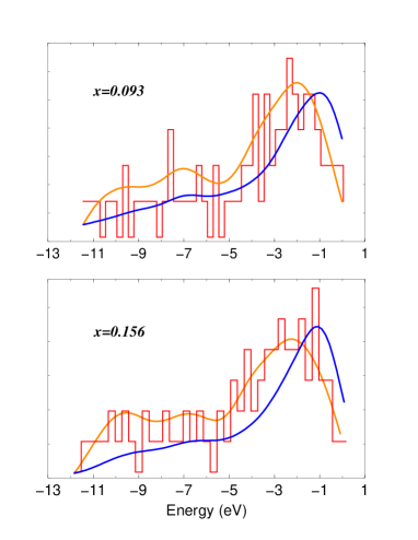
In Fig. 4 we show the total electronic density of states (DOS) and its projection on the covalent and dangling Wannier functions. These show clearly that the dangling states dominate the electronic DOS close to the Fermi level.
These two facts are not in contradiction to a picture in which the conductivity takes place via an hopping mechanism as suggested by the experiments.
In conclusion, we have shown that alloys at low concentrations have a very peculiar electronic structure. The donates its valence electrons to the network and is trapped in cavities. These electrons are trapped in doubly occupied dangling bonds. These defect states can be observed via infra-red spectroscopy. Our study can be a stepping stone for the more complex case of the magnetic alloys. In fact it is likely that many of the features found here will also be present in the case of and contribute to its unusual properties. We could speculate that as the concentration increases the filled cavities interact more and more until the tetrahedrically bonded network of is disrupted and local coordinations like those observed in the stoichiometric compound will dominate the local structure. We plan to address these issues in our forthcoming work.
We thank M. Bernasconi, P. L. Silvestrelli and F. Hellman for stimulating discussions.
REFERENCES
- [1] F. Hellman, M. Q. Tran, A. E. Gebala, E. M. Wilcox and R. C. Dynes, Phys. Rev. Lett. 77, 4652 (1996)
- [2] B. L. Zink, E. Janod, K. Allen and F. Hellnan, Phys. Rev. Lett. 83, 2266 (1999)
- [3] P. Xiong, B. L. Zink, S. I. Applebaum, F. Hellman and R. C. Dynes, Phys. Rev. B 59, 3929 (1999)
- [4] R. Car and M. Parrinello, Phys. Rev. Lett. 55, 2471 (1985).
- [5] CPMD, J. Hutter et. Al. MPI für Festkörperforschung and IBM Zurich Research Laboratory 1995 - 1999.
- [6] S. Goedecker, M. Teter and J. Hutter, Phys. Rev. B 54, 1703 (1996).
- [7] C. Hartwigsen, S. Goedecker and J. Hutter, Phys. Rev. B 58, 3641 (1998).
- [8] R. Car and M. Parrinello Phys. Rev. Lett. 60, 204 (1988); G. Galli, R. M. Martin, R. Car and M. Parrinello, Phys. Rev. Lett. 62, 555 (1989); F. Buda, G. L. Chiarotti, I. Stich, R. Car and M. Parrinello, J. Non-Cryst. Solids 114, 7 (1989); G. Galli, R. M. Martin, R. Car and M. Parrinello, Phys. Rev. B 44, 11092 (1991); F. Finocchi, G. Galli, M. Parrinello and C. M. Bertoni, Phys. Rev. Lett. 68, 3044 (1992); N. A. Marks, D. R. McKenzie, B. A. Pailthorpe, M. Bernasconi and M. Parrinello, Phys. Rev. Lett. 76, 768 (1996); A. Gambirasio M. Bernasconi, Phys. Rev. B 60, 12007 (1999); D. G. McCulloch, D. R. McKenzie and C. M. Goringe, Phys. Rev. B 61, 2349 (2000).
- [9] P. E. Blöchl and M. Parrinello, Phys. Rev. B 45, 9413 (1992).
- [10] N. Marzari and D. Vanderbilt, Phys. Rev. B56, 12847 (1997).
- [11] P. L. Silvestrelli, N. Marzari D. Vanderbilt and M. Parrinello, Sol. State. Comm. 107, 7 (1998).