Side-gate modulation of critical current in mesoscopic Josephson junction
Abstract
We study the normal state conductance and the Josephson current in a superconductor-2DEG-superconductor structure where the size/shape of the 2DEG-region can be modified by an additional side-gate electrode. The considered transport properties follow from the retarded Green function which we compute by employing a tight-binding-like representation of the Hamiltonian in the 2DEG region. Our model studies offer a qualitative demonstration of the recently observed effects caused by side-gate modulation.
keywords:
Josephson effect, Andreev scattering, quantum interference, side-gate modulation1 Introduction
Devices with semiconducting materials as barriers in Josephson weak links offer the possibility to modulate the junction properties in order to investigate both fundamental transport mechanisms as well as for use in applications of superconducting devices. Several methods for tunable Josephson junctions have been studied both theoretically and experimentally. Tunable effects have been observed in e.g. Josephson-field-effect-transistors [1], non-equilibrium junctions [2, 3], optically modulated weak links [4], and recently in side-gate modulated junctions [5].
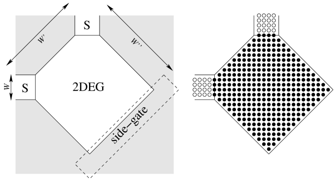
Following Ref. [5] we consider superconductor-2DEG-superconductor structures where the indirect ballistic transport between the non-opposite superconducting contacts can be controlled by a voltage applied to a side-gate (see Fig. 2). The geometry has many similarities with the T-stub wave guide geometry [6, 7] but here the two interfaces to the superconductors are non-opposite. The aim is to demonstrate the principle behind side-gate modulation of the critical current and also to investigate the local density-of-states in the 2DEG in relation to the discussion of “non-local” modes [8, 9].
In this work we focus on the normal state conductance and the Josephson current in the case where electron and hole propagation in the normal region is phase-coherent. For convenience we consider the zero temperature limit. The normal state conductance is then given by the Landauer formula [10, 11, 12] which at has the particularly simple form
| (1) |
where is the quantum unit of conductance and () are the transmission eigenvalues of which is an matrix, being the number of propagating modes at the Fermi level. Beenakker and van Houten [13] considered the Josephson current through a superconducting quantum point contact and found that the critical current was quantized in units of , being the energy gap of the superconductor. Subsequently it was shown by Beenakker [14] that just like the normal state conductance, also the Josephson current between two superconducting leads can also be expressed in terms of of the normal region which couples the two superconductors. At the Josephson current can be written as [14]
| (2) | |||||
where is the phase difference between the two superconductors. Eq. (2) is valid in the short-junction limit where the dimension of the normal region is short compared to the superconducting coherence length which in the ballistic regime is , being the Fermi velocity.
We note that in Eqs. (1) and (2) all transverse degrees-of-freedom are incorporated in the transmission amplitude matrix and that the angle-dependence of the Andreev scattering discussed in Ref. [15] follows directly from the angle (mode) dependence of . Scattering due to non-matching Fermi velocities or Fermi momenta can be included in several ways: i) by calculating the transmission from the composite scattering matrix where the two interfaces ( and ) are described by the scattering matrices and as in Ref. [16], ii) by adding an effective potential to the 2DEG at the interfaces, or iii) by explicitly taking the different Fermi velocities and Fermi momenta into account. In this work we will however for simplicity assume matching Fermi properties of the superconductor and the 2DEG.
To illustrate how the transport properties depend on the transmission let us consider the case of single-mode leads. Fig. 1 shows how the normal state conductance , the critical current , and the product depend on the transmission probability . Compared to the off-resonance regime with (the Ambegaokar–Baratoff regime [17]) the product is enhanced by a factor-of-two when the 2DEG region is tuned to resonance (). This factor-of-two enhancement can be considered as a signature of Andreev mediated transport at resonance whereas the transport is tunneling-like at off-resonance.
Equations (1) and (2) form the basis for our calculations of the transport properties and since they only depend on the normal state transmission properties of the 2DEG region we can employ standard methods for quantum transport in semiconductor structures. The transmission can conveniently be calculated from the retarded Green function [12] and also the local density-of-states follows from . We calculate by applying a finite differences method to the Hamiltonian of the 2DEG region.

2 Finite differences method
We discretize the continuous Hamiltonian by writing the Laplacian as finite differences [18]. This gives rise to a tight-binding-like representation
where is the number of nearest neighbors (NN) and corresponds to a hopping matrix element, being the lattice spacing. Comparing the energy dispersion to the parabolic dispersion of the continuous problem shows that the finite differences method is a very accurate description for energies [18, 19]. Making the grid finer ( smaller) improves the accuracy and/or allows for a treatment of higher energies.
With the above definition of the Hamiltonian we label the lattice points by a number from to , being the number of lattice points. The retarded Green function can then be written as an matrix [18, 19]
| (4) |
where the element corresponds to . Here, is the tight-binding Hamiltonian of the conductor (describing the conductor as a closed system) and is the self-energy describing the coupling to leads and . For the self-energies the only non-zero elements are those where the leads couple to the 2DEG (scattering region). For large it can be useful to employ a recursive method for calculating but even for the direct matrix inversion in Eq. (4) can be done without too much numerical effort.
The transmission amplitude matrix can now be calculated from the Fisher–Lee relation [12] which gives [12, 18, 19, 20]
| (6) |
and
where we have used the cyclic invariance of the trace. Once the retarded Green has been obtained (by a single matrix inversion) these relations directly provide the essential transport properties. The local density-of-states (in the normal state) can also be calculated directly from the retarded Green function (see e.g. [18])
| (8) |
and this function is useful in obtaining insight into the spatial variations of the states and revealing the nature of the conduction through the sample.
3 Geometry and model
We consider the geometry shown in Fig. 2. The 2DEG is confined also in the direction parallel to the side-gate so that the system acts as a cavity or quantum dot coupled to two superconductors and an additional side-gate. We note that our geometry is slightly different from that of Ref. [5] where there is no confinement of the 2DEG in the direction parallel to the side-gate. This means that here the side-gate is used in tuning the cavity to resonance whereas in Ref. [5] it rather acts as a ’classical’ mirror which can be used in focusing the incident wave from one lead onto the other lead.
We treat the transmission problem fully quantum mechanically by means of the presented finite differences method and the lattice version of the sample shown in Fig. 2. In this case with sites in the transverse direction of the leads of width . In the continuous description of the leads gives the number of propagating modes at the Fermi level, being the integer part of . The dimensions are and . We choose and the Fermi level such that . The lattice model then gives a reasonable description of the continuous problem – the threshold energy of the first mode deviates only by from the continuous result.
The side-probe is assumed to act as a gate and only affect the potential of the 2DEG through an electro-static coupling. Here, we note that fluctuations in the gate potential may lead to dephasing of the electron and hole propagation in the 2DEG (see e.g. Ref. [21]) and the same can also be the case if the probe acts as a voltage probe (see e.g. Ref. [22]). Here, we use the model in Ref. [23] [Eq. (19)] to account for the potential modification in the 2DEG due to the side-gate. The distance from the side-gate to the 2DEG edge position is then given by
| (9) |
where is the side-gate voltage, is the dielectric constant of the semiconductor ( for GaAs), and the 2DEG density. With the lattice shown in Fig. 2 the distance can be changed in steps of corresponding to .
4 Results
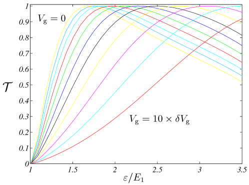
In Fig. 3 we show the transmission as a function of the energy for different values of the gate voltage. Since the interfaces between the leads and the 2DEG are fully transparent the transmission shows a broad resonance behavior. By changing the gate voltage the cavity is ’squeezed’ and as expected the resonance shifts towards higher energies. For a given Fermi level the side-gate can thus also be used in tuning the transmission to resonance.
In Fig. 4 we show the normal state conductance , the critical current , and the product as a function of gate voltage for an energy . By increasing the gate voltage the cavity is tuned to resonance at where the normal state conductance equals the quantum unit of conductance and the critical current equals the quantum unit of critical current . The product changes by a factor-of-two from the Ambegaokar–Baratoff value to its quantum unit at resonance.
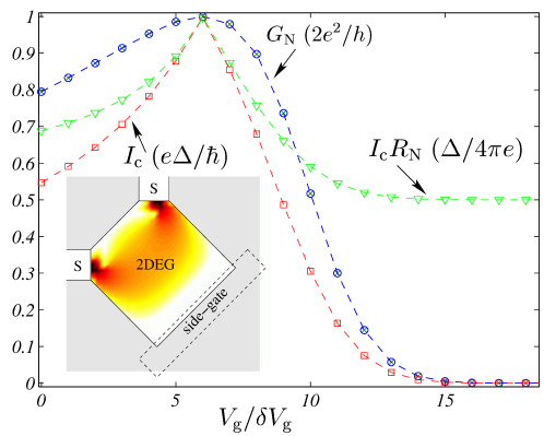
In the inset of Fig. 4 we show the local density of states (in the normal state) at the energy for a gate voltage corresponding to the resonance condition. The transparent interfaces give rise to a local density of states forming a relatively smooth and connected ’path’ between the two leads. The plot also clearly shows the wave nature of the electron and hole propagation. Thus a more simple semi-classical trajectory model with point-like particles and a side-gate acting as a classical mirror would be inadequate for the present situation. This is often the case and as studied in e.g. Ref. [24] complicated multiple scattering processes can in a full quantum mechanical treatment give rise to effects not found in a semi-classical study.
5 Discussion and conclusion
Hybrid semiconductor-superconductor structures offer interesting possibilities for investigating fundamental transport phenomena as well as for potential applications. We have studied the possibility of side-gate modulating the critical current in a mesoscopic superconductor-2DEG-superconductor Josephson junction. Side-gate modulation offers a new alternative to devices based on field-effects, non-equilibrium effects, and optical effects. In the case of side-gate modulation the side-gate is used in tuning the transmission of the 2DEG to resonance.
Our calculations are based on a numerical treatment of the transmission properties of the 2DEG region. Using the Landauer formula [10, 11, 12] and a similar formula for the Josephson current [14] we have then calculated the essential transport properties: the normal state conductance , the critical current , and the product. The conductance in the superconducting state can unfortunately not be expressed directly in terms of the transmission eigenvalues and is complicated due to the presence of multiple Andreev reflections (see however Ref. [25] for a possible solution). The considered geometry is comparable to the situation in recent experiments [5] even though some simplifications have been made. A quantitative comparison would require i) that the different Fermi properties of the superconductor and the 2DEG are taken into account [15], ii) more lattice points () in order to account correctly for the case of multi-mode leads ( in Ref. [5]), and iii) that the width of the 2DEG should be much larger than the separation of the two leads. However, our model studies demonstrate how the side-gate modulation can be used in controlling both the normal state conductance and the critical current.
Our results are in qualitative agreement with the recent experimental findings [5] and confirm the possibility of modulating the transport properties by a side-gate. Studies of the local density of states confirm the existence of “non-local” modes and indicate that more simple trajectory models can not fully account for the detailed electron and hole propagation – rather a full quantum mechanical treatment is necessary.
Acknowledgements — We would like to thank M. Brandbyge, A.-P. Jauho, K. Flensberg, and H. Takayanagi for useful discussions.
References
- [1] T. D. Clark, R. J. Prance, and A. D. C. Grassie, J. Appl. Phys. 51, 2736 (1980).
- [2] A. Morpurgo, B. J. van Wees, and T. M. Klapwijk, Appl. Phys. Lett. 72, 966 (1998).
- [3] J. Kutchinsky et al., Phys. Rev. Lett. 83, 4856 (1999).
- [4] G. Bastian et al., Appl. Phys. Lett. 75, 94 (1999).
- [5] G. Bastian and H. Takayanagi, Physica C, submitted (2000). [cond-mat/0005435]
- [6] F. Sols, M. Macucci, U. Ravaioli, and K. Hess, J. Appl. Phys. 66, 3892 (1989).
- [7] K. Aihara, M. Yamamoto, and T. Mizutani, Appl. Phys. Lett. 63, 3595 (1993).
- [8] J. P. Heida, B. J. van Wees, T. M. Klapwijk, and G. Borghs, Phys. Rev. B 57, 5618 (1998).
- [9] G. Bastian et al., Phys. Rev. Lett. 81, 1686 (1998).
- [10] R. Landauer, Phil. Mag. 21, 863 (1970).
- [11] R. Landauer, IBM J. Res. Dev. 1, 223 (1957).
- [12] D. S. Fisher and P. A. Lee, Phys. Rev. B 23, 6851 (1981).
- [13] C. W. J. Beenakker and H. van Houten, Phys. Rev. Lett. 66, 3056 (1991).
- [14] C. W. J. Beenakker, Phys. Rev. Lett. 67, 3836 (1991), ibid 68, 1442 (1992).
- [15] N. A. Mortensen, K. Flensberg, and A.-P. Jauho, Phys. Rev. B 59, 10176 (1999).
- [16] N. A. Mortensen, A.-P. Jauho, K. Flensberg, and H. Schomerus, Phys. Rev. B 60, 13762 (1999).
- [17] V. Ambegaokar and A. Baratoff, Phys. Rev. Lett. 10, 486 (1963), ibid 11, 104 (1963).
- [18] S. Datta, Electronic Transport in Mesoscopic Systems (Cambridge University Press, Cambridge, 1995).
- [19] D. K. Ferry and S. M. Goodnick, Transport in Nanostructures (Cambridge University Press, Cambridge, 1997).
- [20] M. Brandbyge, N. Kobayashi, and M. Tsukada, Phys. Rev. B 60, 17064 (1999).
- [21] M. Büttiker and A. M. Martin, Phys. Rev. B 61, 2737 (2000).
- [22] N. A. Mortensen, A.-P. Jauho, and K. Flensberg, Superlattice Microst., in press (2000), [cond-mat/9909029].
- [23] L. I. Glazman and I. A. Larkin, Semicond. Sci. Technol. 6, 32 (1991).
- [24] A.-P. Jauho, K. N. Pichugin, and A. F. Sadreev, Phys. Rev. B 60, 8191 (1999).
- [25] G. Johansson, G. Wendin, K. N. Bratus, and V. S. Shumeiko, Superlattice Microst. 25, 905 (1999).