Circuit theory of multiple Andreev reflections in diffusive SNS junctions: the incoherent case
Abstract
The incoherent regime of Multiple Andreev Reflections (MAR) is studied in long diffusive SNS junctions at applied voltages larger than the Thouless energy. Incoherent MAR is treated as a transport problem in energy space by means of a circuit theory for an equivalent electrical network. The current through NS interfaces is explained in terms of diffusion flows of electrons and holes through “tunnel” and “Andreev” resistors. These resistors in diffusive junctions play roles analogous to the normal and Andreev reflection coefficients in OTBK theory for ballistic junctions. The theory is applied to the subharmonic gap structure (SGS); simple analytical results are obtained for the distribution function and current spectral density for the limiting cases of resistive and transparent NS interfaces. In the general case, the exact solution is found in terms of chain-fractions, and the current is calculated numerically. SGS shows qualitatively different behavior for even and odd subharmonic numbers , and the maximum slopes of the differential resistance correspond to the gap subharmonics, . The influence of inelastic scattering on the subgap anomalies of the differential resistance is analyzed.
I Introduction
The concept of multiple Andreev reflections (MAR) was first introduced by Klapwijk, Blonder, and Tinkham [1] in order to explain the subharmonic gap structure (SGS) on current-voltage characteristics of superconducting junctions. The theory was originally formulated for perfect SNS junctions and then extended to include the effect of resistance of the SN interface[2] (OTBK theory). Within this approach, the subgap current transport is described in terms of ballistic propagation of quasiclassical electrons through the normal metal region, accompanied by Andreev and normal reflections from specular NS boundaries. During every passage across the junction, the electrons and the retro-reflected holes gain energy equal to , which allows them eventually to escape from the SNS well. This energy gain results in strong quasiparticle nonequilibrium within the subgap energy region .
OTBK theory gives a qualitatively adequate description of dc current transport in voltage biased SNS junctions; however, its quantitative results have a rather limited range of applicability. In short ballistic junctions with length comparable with or smaller than the coherence length (e.g., atomic-size junctions), the quantum coherence of subsequent Andreev reflections plays a crucial role leading to the ac Josephson effect. It has been shown that such a coherence also strongly modifies the dc current and SGS [3, 4] (coherent MAR regime). In fact, even in long ballistic SNS junctions (e.g. 2DEG-based devices), the coherence effects are important and give rise to resonant structures in the current due to Andreev quantization. In this respect, the quasiclassical OTBK theory, which does not include any coherence effects, may be qualified as a model for the incoherent MAR regime.
One might expect that impurities could provide the conditions for incoherent MAR by washing out the Andreev spectrum. However, this is not the case for a short diffusive junction, where appreciable Josephson coupling gives rise to coherent MAR.[5, 6] The electron-hole coherence in the normal metal holds over a distance of the coherence length from the superconductor ( is the diffusion constant). The overlap of coherent proximity regions induced by both SN interfaces creates an energy gap in the electron spectrum of the normal metal, which plays the role of the level spacing in the ballistic case. In short junctions with a wide proximity gap of the order of the energy gap in the superconducting electrodes, the phase coherence covers the entire normal region.
An incoherent MAR regime will occur in long diffusive SNS junctions with a small proximity gap of the order of Thouless energy .[7] If the applied voltage is large on a scale of the Thouless energy, , then the coherence length is much smaller than the junction length at all relevant energies . In this case, the proximity regions near the SN interfaces become virtually decoupled and the Josephson oscillations are strongly suppressed. At the same time, as soon as the inelastic mean free path exceeds the junction length, the subgap electrons must undergo many incoherent Andreev reflections before they enter the reservoir. We emphasize that such incoherency is provided by the small coherence length at large enough voltages, while the intrinsic dephasing length can be arbitrarily large. In order to describe such an incoherent MAR regime, one has to operate with the electron and hole diffusion flows across the junction rather than with ballistic quasiparticle trajectories, and to consider the Andreev reflections as the relationships between these diffusive flows.
The first step in extending the OTBK approach to diffusive SNS structures was taken by Volkov and Klapwijk,[8] who derived recurrence relations between the boundary values of the distribution functions. In that study, only a weak nonequilibrium was considered, which implies suppression of MAR by inelastic relaxation. In the present paper, we focus on the opposite case of strong nonequilibrium in the developed MAR regime, which results in the appearance of SGS on - characteristics of the diffusive SNS junctions.[9] Following the interpretation of MAR as a transport problem in energy space[7, 10], we analyze it by formulating an equivalent network in the spirit of Nazarov’s circuit theory.[11] Within this approach, the energy-dependent tunnel and Andreev resistances of an equivalent circuit play roles similar to the normal and Andreev reflection probabilities in OTBK theory, and the effective voltage source is represented by Fermi reservoirs.
The paper is organized as follows. In Section II, we derive the equations for incoherent MAR from the general Keldysh equations. In Sections III and IV, the circuit representation is formulated; some applications are considered in Section V. The SGS in junctions with resistive interfaces is calculated in Section VI. The complete solution of the problem suitable for numerical calculation of the - characteristics is obtained in Section VII by using a chain-fraction technique.[4] In Section VIII, we discuss limitations on the MAR regime imposed by inelastic processes.
II Microscopic background
The system under consideration consists of a normal channel () confined between two voltage biased superconducting electrodes, with the elastic mean free path much shorter than any characteristic size of the problem. In this limit, the microscopic analysis of current transport can be performed within the framework of the diffusive equations of nonequilibrium superconductivity[12] for the supermatrix Keldysh-Green function :
| (1) |
| (2) |
where is the modulus and is the phase of the order parameter, and is the electric potential. The Pauli matrices operate in the Nambu space of matrices denoted by “hats”, and the products of two-time functions are interpreted as their time convolutions. The junction length is assumed to be smaller than the inelastic and phase-breaking lengths, which allows us to exclude the inelastic collisions from our consideration at this stage; their role will be discussed later. The electric current per unit area is expressed through the Keldysh component of the supermatrix current :
| (3) |
where is the conductivity of the normal metal.
At the SN interface, the supermatrix satisfies the boundary condition[13]
| (4) |
where the indices denote the right and left sides of the interface and is the interface resistance per unit area in the normal state, which relates to, e.g., a Schottky barrier or mismatch between the Fermi velocities. Within the model of infinitely narrow potential of the interface barrier, , the interface resistance is related to the barrier strength as .[14] It has been shown in Ref. [15] that Eq. (4) is valid either for a completely transparent interface (, ) or for an opaque barrier whose resistance is much greater than the resistance of a metal layer with the thickness formally equal to .
According to the definition of the supermatrix ,
| (5) |
Eqs. (1) and (4) represent a compact form of separate equations for the retarded and advanced Green’s functions and the distribution function . Their time evolution is imposed by the Josephson relation for the phase of the order parameter in the right electrode (we assume in the left terminal). This implies that the function consists of a set of harmonics , , which interfere in time and produce the ac Josephson current. However, when the junction length is much larger than the coherence length at all relevant energies , we may consider coherent quasiparticle states separately at both sides of the junction, neglecting their mutual interference and the ac Josephson effect. Thus, the Green’s function in the vicinity of left SN interface can be approximated by the solution of the static Usadel equations for a semi-infinite SN structure,[16] with the spectral angle satisfying the equation
| (6) |
with the boundary condition
| (7) |
The indices , in these equations refer to the superconducting and the normal side of the interface, respectively.
The dimensionless parameter in Eq. (7),
| (8) |
where is the resistance of the normal channel per unit area, has the meaning of an effective barrier transmissivity for the spectral functions.[17] Note that even at large barrier strength ensuring the validity of the boundary conditions Eq. (4),[15] the effective transmissivity of the barrier in a “dirty” system, , could be large. In this case, the spectral functions are virtually insensitive to the presence of a barrier and, therefore, the boundary conditions Eqs. (4) can be applied to an arbitrary interface if we approximately consider high-transmissive interfaces with as completely transparent, . For low transmissivity, , Eq. (7) can be analyzed within a perturbative approach (see the Appendix). At arbitrary , Eq. (7) should be solved numerically.
The distribution functions are to be considered as global quantities within the whole normal channel determined by the diffusive kinetic equations
| (9) |
with dimensionless diffusion coefficients
| (11) |
| (12) |
Assuming the normal conductance of electrodes to be much greater than the junction conductance, we consider them as equilibrium reservoirs with unperturbed spectral characteristics, , and equilibrium quasiparticle distribution, . Within this approximation, the boundary conditions for the distribution functions in Eq. (9) at read
| (13) |
| (14) |
where
| (15) |
| (16) |
At large energies, , when the normalized density of states approaches unity and the condensate spectral functions turn to zero at both sides of the interface, the conductances coincide with the normal barrier conductance; within the subgap region , .
Similar considerations are valid for the right NS interface, if we eliminate the explicit time dependence of the order parameter in Eq. (1), along with the potential of right superconducting electrode, by means of a gauge transformation[18]
| (17) |
As a result, we arrive at the same static equations and boundary conditions, Eqs. (6)-(16), with , for the gauge-transformed functions and . Thus, to obtain a complete solution for the distribution function , which determines the dissipative current
| (18) |
we must solve the boundary problem for at the left SN interface, and a similar boundary problem for at the right interface, and then match the distribution function asymptotics deep inside the normal region by making use of the relationship following from Eqs. (5), (17):
| (19) |
III Circuit representation of boundary conditions
In order for this kinetic scheme to conform to the conventional physical interpretation of Andreev reflection in terms of electrons and holes, we introduce the following parameterization of the matrix distribution function,
| (20) |
where and will be considered as the electron and hole population numbers. Deep inside the normal metal region, they acquire rigorous meaning of distribution functions of electrons and holes. In equilibrium, the functions approach the Fermi distribution. In this representation, Eqs. (9) take the form
| (21) |
where , and they may be interpreted as conservation equations for the (specifically normalized) net probability current of electrons and holes, and for the electron-hole imbalance current . Furthermore, the probability currents of electrons and holes, defined as , separately obey the conservation equations. The probability currents are naturally related to the electron and hole diffusion flows, , at large distances from the SN boundary. Within the proximity region, , each current generally consists of a combination of both the electron and hole diffusion flows,
| (22) |
which reflects coherent mixing of normal electron and hole states in this region.
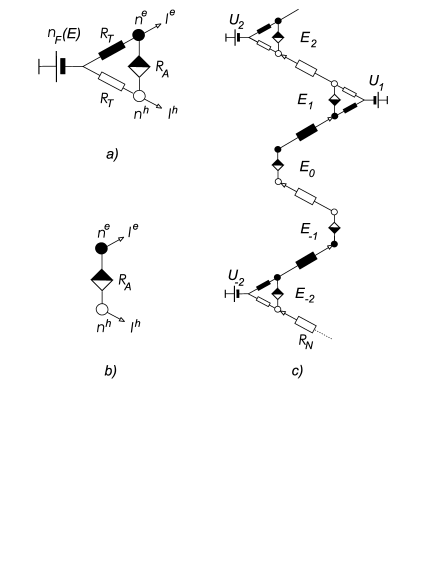
Each of the equations Eq. (23) may be clearly interpreted as a Kirchhoff rule for the electron or hole probability current flowing through the effective circuit (tripole) shown in Fig. 1(a). Within such an interpretation, the nonequilibrium populations of electrons and holes at the interface correspond to “potentials” of nodes attached to the “voltage source” – the Fermi distribution in the superconducting reservoir – by “tunnel resistors” . The “Andreev resistor” between the nodes provides electron-hole conversion (Andreev reflection) at the SN interface.[19]
The circuit representation of the diffusive SN interface is analogous to the scattering description of ballistic SN interfaces: the tunnel and Andreev resistances in the diffusive case play the same role as the normal and Andreev reflection coefficients in the ballistic case.[14] For instance, for [Fig. 1(a)], the probability current is contributed by equilibrium electrons incoming from the superconductor through the tunnel resistor , and also by the current flowing through the Andreev resistor as the result of hole-electron conversion. Within the subgap region, , [Fig. 1(b)], the quasiparticles cannot penetrate into the superconductor, , and the voltage source is disconnected, which results in detailed balance between the electron and hole probability currents, (complete reflection). For the perfect interface, turns to zero, and the electron and hole population numbers become equal, (complete Andreev reflection). The nonzero value of the Andreev resistance for accounts for suppression of Andreev reflection due to the normal reflection by the interface.
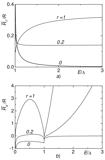
Detailed information about the boundary resistances can be obtained from asymptotic expressions for the bare interface resistances (see the Appendix) and numerical plots of in Fig. 2. In particular, turns to zero at the gap edges due to the singularity in the density of states which enhances the tunneling probability. Furthermore, the imbalance resistance approaches the normal value at due to the enhancement of the Andreev reflection at small energies, which results from multiple coherent backscattering of quasiparticles by the impurities within the proximity region. This property is the reason for the re-entrant behavior of the conductance of high-resistive SIN systems[8, 20] at low voltages. In the MAR regime, one cannot expect any reentrance since quasiparticles at all subgap energies participate in the charge transport even at small applied voltage.
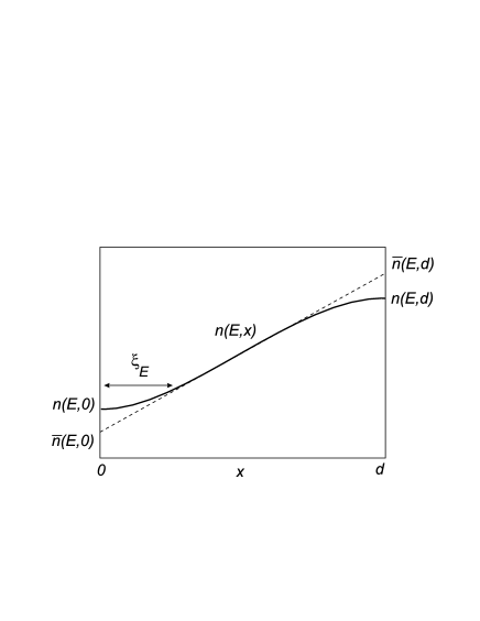
The diffusion coefficients in Eq. (9) turn to unity far from the SN boundary, and therefore the population numbers become linear functions of ,
| (25) |
This equation defines the renormalized population numbers at the NS interface, which differ from due to the proximity effect, as shown in Fig. 3. These quantities have the meaning of the true electron/hole populations which would appear at the NS interface if the proximity effect had been switched off. It is possible to formulate the boundary conditions in Eq. (23) in terms of these population numbers by including
the proximity effect into renormalization of the tunnel and Andreev resistances. To this end, we will associate the node potentials with renormalized boundary values of the population numbers, where are found from the exact solutions of Eqs. (21),
| (26) |
Here are the proximity corrections to the normal metal resistance at given energy for the probability and imbalance currents, respectively,
| (28) |
| (29) |
see the insets in Fig. 2(a,b). It follows from Eq. (26) that the same Kirchhoff rules as in Eqs. (23), (24) hold for and , if the bare resistances are substituted by the renormalized ones,
| (30) |
The energy dependence of the renormalized boundary resistances and is illustrated in Fig. 4. In some cases, there is an essential difference between the bare and renormalized resistances, which leads to qualitatively different properties of the SN interface for normal electrons and holes compared to the properties of the bare boundary. Let us first discuss a perfect SN interface with . Within the subgap region , the bare tunnel resistance is infinite whereas the bare Andreev resistance turns to zero; this corresponds to complete Andreev reflection, as already explained. However, the Andreev resistance for normal electrons and holes, , is finite and negative,[21] which leads to enhancement of the normal metal conductivity within the proximity region.[20, 22] At , the bare tunnel resistance is zero, while the renormalized tunnel resistance is finite (though rapidly decreasing at large energies). This leads to suppression of the probability currents of normal electrons and holes within the proximity region, which is to be attributed to the appearance of Andreev reflection. Such a suppression is a global property of the proximity region in the presence of sharp spatial variation of the order parameter, and it is similar to the over-the-barrier Andreev reflection in the ballistic systems. In the presence of normal scattering at the SN interface, the overall picture depends on the interplay between the bare interface resistances and the proximity corrections ; for example, the renormalized tunnel resistance diverges at , along with the proximity correction , in contrast to the bare tunnel resistance . This indicates complete Andreev reflection at the gap edge independently of the transparency of the barrier, which is similar to the situation in the ballistic systems where the probability of Andreev reflection at is always equal to unity.
IV Assembling MAR networks
To complete the definition of an equivalent MAR network, we have to construct a similar tripole for the right NS interface and to connect boundary values of population numbers (node potentials) using the matching condition Eq. (19) expressed in terms of electrons and holes:
| (31) |
Since the gauge-transformed distribution functions obey the same equations Eq. (9)-(16), the results of the previous Section can be applied to the functions and (the minus sign implies that is associated with the current incoming to the right-boundary tripole). In particular, the asymptotics of the gauge-transformed population numbers far from the right interface are given by the equation
| (32) |
After matching the asymptotics in Eqs. (25) and (32) by means of Eq. (31), we find the following relations:
| (33) |
| (34) |
From the viewpoint of the circuit theory, Eq. (34) may be interpreted as Ohm’s law for the resistors which connect energy-shifted boundary tripoles, separately for the electrons and holes, as shown in Fig. 1(c).
The final step which essentially simplifies the analysis of the MAR network, is based on the following observation. The spectral probability currents yield opposite contributions to the electric current in Eq. (18),
| (35) |
due to the opposite charge of electrons and holes. At the same time, these currents, referred to the energy axis, transfer the charge in the same direction, viz., from bottom to top of Fig. 1(c), according to our choice of positive . Thus, by introducing the notation for an electric current entering the node with the energy , as shown by arrows in Fig. 1(c),
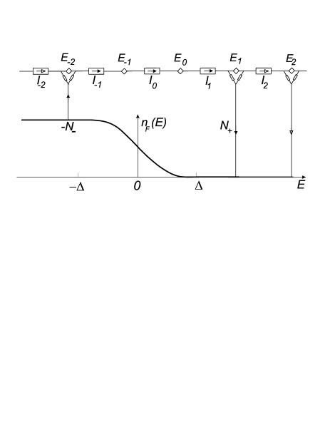
| (36) |
we arrive at an “electrical engineering” problem of current distribution in an equivalent network in energy space plotted in Fig. 5, where the difference between electrons and holes becomes unessential. The bold curve in Fig. 5 represents a distributed voltage source – the Fermi distribution connected periodically with the network nodes. Within the gap, , the nodes are disconnected from the Fermi reservoir and therefore all partial currents associated with the subgap nodes are equal.
Since all resistances and potentials of this network depend on , the partial currents obey the relationship which allows us to express the physical electric current, Eq. (35), through the sum of all partial currents flowing through the normal resistors , integrated over an elementary energy interval :
| (37) |
| (38) |
The spectral density is periodic in with the period and symmetric, , which follows from the symmetry of all resistances with respect to .
As soon as the partial currents are found, the population numbers can be recovered by virtue of Eqs. (21), (23), (25), and (36):
| (39) |
| (40) |
at . Within the subgap region, Eq. (40) is inapplicable due to the undeterminacy of product . In this case, one may consider the subgap part of the network as a voltage divider between the nodes nearest to the gap edges, having the numbers , , respectively, where , Int() denoting the integer part of . Then the boundary populations at become
| (41) | |||||
| (42) |
where indicate the right (left) node of the tripole, irrespectively of whether it relates to the left (even ) or right (odd ) interface. The physical meaning of , however, depends on the parity of :
| (43) |
The values in Eq. (41) can be found from Eq. (40) which is generalized for any tripole of the network in Fig. 5 outside the gap as
| (44) | |||
| (45) |
The circuit formalism can be simply generalized to the case of different transparencies of NS interfaces, as well as to different values of in the electrodes. In this case, the network resistances become dependent not only on but also on the parity of . As a result, the periodicity of the current spectral density doubles: , and, therefore, is to be integrated in Eq. (37) over the period , with an additional factor .
V Simple applications
A helpful example of an asymmetric junction which allows us immediately to obtain an analytical solution is given by the SNN structure. The problem of calculation of its conductivity is inherently static and therefore may be completely solved for any junction length. If the latter is much larger than the coherence length, the circuit approach of the previous Section is applicable without restrictions. Due to the absence of superconducting correlations at the right NN interface, odd Andreev resistors are eliminated and, therefore, the whole network may be split into separate finite circuits located around even (superconducting) nodes, as shown in Fig. 6(a); moreover, odd tunnel resistances are to be considered as normal ones. After some simple algebra, we obtain the sum of partial currents in each subcircuit,
| (46) |
which leads to a well known formula for the - characteristics of a long SNN junction:[8]
| (47) | |||
| (48) |
If the junction is short enough ( and are comparable), one might naively expect some kind of proximity-induced Andreev scattering at the right NN interface, followed by MAR and SGS anomalies in the - characteristic. However, the circuit theory rejects this assumption at once: since the condensate spectral functions , Eq. (16), disappear in the normal terminal, the conductivities become equal, and the Andreev channel becomes closed () at the NN interface at any length of the junction. Thus, the circuit model of charge transport in Fig. 6(a) remains valid, with a few modifications: (i) the spectral angle has to be found from the Usadel equation for the finite interval , (ii) the proximity corrections at the left SN interface are to be expressed through the integrals
| (49) |
instead of Eq. (26), and (iii) odd tunnel resistances should be replaced by the energy-dependent bare resistances [or, equivalently, ]. From this point of view, the entire channel represents a global “Andreev reflector” for normal electrons and holes incoming from the right reservoir.
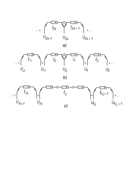
The next simple application of this circuitry is given by calculation of the excess (deficit) current in SNS junctions, i.e., the difference between the currents in superconducting and normal state at large voltages . Assuming the integration in Eq. (37) to be reduced to the interval by making use of the symmetry , we note that the Andreev conductances are negligibly small for all nodes with (). Thus, the circuit in Fig. 5 may be split, as in the case of the SNN junction discussed above, into the chain of separate circuits shown in Fig. 6(b). The contribution of the central circuit is described by Eq. (46) with , whereas the other parts are to be considered as normal circuits and represent contribution of thermally excited quasiparticles:
| (50) |
where is the net normal resistance of the junction. In summary, we obtain another well-known result,[20]
| (51) | |||
| (52) |
It is of interest to note that the net resistance for the probability current never enters final results in these examples and, therefore, the superconducting modification involves only the imbalance resistance . In other words, only the evolution of the imbalance between the electron and hole populations is relevant for the charge transport in such cases.
VI MAR transport
Proceeding with the analysis of current transport through the SNS junction at arbitrary voltages, we first discuss the case of low-transparent barriers, . We note that in practice this case is relevant for a wide range of junctions both with high interface resistance, , and comparatively low interface resistance . Indeed, according to Eq. (8), the ratio , being proportional to , contains also the large parameter . Therefore, the limit covers most of the practically interesting situations, , and only the case of very small interface resistances, , requires special consideration.
At , the proximity effect is essentially suppressed and the calculations can be performed on the basis of a simplified model of the equivalent network, which nevertheless provides a quantitative description of . Due to the sharp increase in the Andreev resistance at [see Fig. 4(b)], all Andreev resistors outside the gap can be excluded, and we arrive at the sequence of subcircuits shown in Fig. 6(c). The central circuit between the nodes and includes normal and Andreev resistors within the gap, as well as two tunnel resistors at the circuit edges. The total resistance of this circuit is
| (53) | |||
| (54) |
and the current through this circuit is given by Ohm’s law:
| (55) |
Thus, the contribution of this circuit to the current spectral density, Eq. (38), is .
The current of thermal excitations is carried by the side circuits (, ):
| (56) |
From Eq. (55) we obtain a simple formula at :
| (57) |
where has the meaning of the effective resistance of the subgap region for the physical electric current.
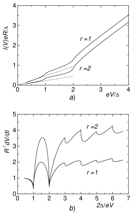
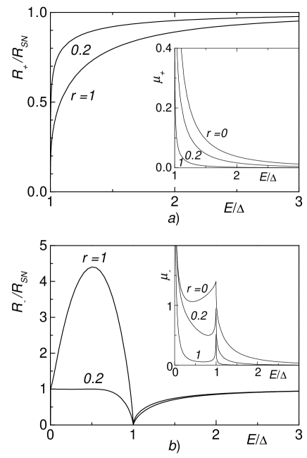
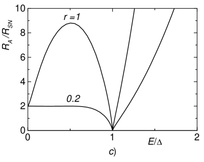
In Fig. 7 we present the - characteristics and the differential resistance vs inverse voltage at zero temperature, calculated numerically by means of Eq. (57). The parameter was chosen to be equal to and at , which corresponds to the resistance ratio equal to and , respectively. In our calculation of in Eq. (53), we used the asymptotic Eq. ( ‣ Circuit theory of multiple Andreev reflections in diffusive SNS junctions: the incoherent case) for the bare resistances at , neglecting small proximity corrections , Eq. (93). The results are in good agreement with those obtained on the basis of exact calculations [see further Eq. (83)]. The smeared steps in the - characteristic indicate steplike increase in the number of subgap Andreev resistors in Eq. (53). The sharp peaks (dips) in arise from the rapidly varying contribution of the nodes which simultaneously cross the gap edges, and therefore both the edge Andreev resistances undergo strong suppression. A certain contribution also comes from the edge tunnel resistances which also show singular behavior at . The peaks are more pronounced for even subharmonics, when the middle Andreev resistor crosses the Fermi level, , and its value is suppressed simultaneously with the edge Andreev resistors. Careful analysis shows that at the gap subharmonics, , the second derivative has sharp maxima.
The magnitude of strongly depends on the number of large Andreev resistors which contribute to . At , at least one Andreev resistor appears far from the “resonant” points where sharply decreases. Thus, the net subgap resistance remains large () at any energy, which results in large differential resistance at these voltages. In the vicinity of the second subharmonic, , the current transport involves a high-transmissive circuit with three Andreev resistors located near the resonant points, which yields a much smaller value of . The same effect occurs at when the resonant circuit contains two suppressed Andreev resistances at the gap edges. At the differential resistance is basically determined by quasiparticles which overcome the energy gap without Andreev reflections, and it turns to the normal value at large voltages.
At low voltage, the amplitude of the oscillations of the differential resistance decreases and the asymptotic value of at can be found analytically from Eqs. (53), (57), by replacing the sum in Eq. (53) with an energy-independent integral. As a result we get
| (58) |
Since each circuit in Fig. 6(c) represents a separate voltage divider, we easily obtain the boundary values of the population numbers. If the node belongs to the central circuit ( for electrons and for holes), we have
| (59) | |||
| (60) |
and, in the opposite case,
| (61) |
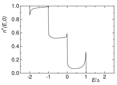
As follows from Eqs. (59), (61), at low temperatures, the energy distribution of quasiparticles within the region has a steplike form (Fig. 8), which is qualitatively similar to, but quantatively different from, that found in OTBK theory.[2] The number of steps increases at low voltage, and the shape of the distribution function becomes resemblant to a “hot electron” distribution with the effective temperature of the order of . This distribution is modulated due to the discrete nature of the heating mechanism of MAR, which transfers the energy from an external voltage source to the quasiparticles by energy quanta . Since the subgap probability current , Eq. (55), is strongly suppressed by large subgap resistance , the spatial variations of the population numbers, Eqs. (25), (39), are negligibly small: .
VII Exact solution
In the case of high transmittance of the NS interface, the partial currents outside the gap noticeably contribute to the net electric current even at . In this case, the - curves should be calculated on the basis of the exact solution of the recurrence relations between partial currents,
| (62) |
following from the Kirchhoff rules for an infinite network in Fig. 5. Here and
| (64) |
| (65) |
By analogy with differential equations, we introduce the following ansatz:
| (66) |
where are the fundamental solutions of the corresponding uniform equation, decreasing at , respectively,
| (68) |
| (69) |
. The quantities
| (70) |
are expressed through the products of chain fractions, , , defined by the recurrences
| (72) |
| (73) |
with the boundary conditions , . Within the gap, , where , the values , are equal to , in accordance with the conservation of the subgap currents mentioned above.
The coefficients in Eq. (66) satisfy an equation following from Eqs. (62), (66), (66),
| (74) | |||
| (75) |
for (and similar for ), where . The requirement of cancellation of terms with in Eq. (74) allows us to completely determine . This yields first-order recurrences for which lead to the formula for partial currents at ,
| (76) |
| (77) |
The undeterminacy of , in Eq. (77) within the subgap region [where and , see Eq. (73)], is resolved by the recurrences , following from Eqs. (70) for . These recurrences are to be continued until the nodes and , respectively, are reached. As a result, we obtain a convenient representation for at :
| (78) |
The effective subgap resistance determined by the denominator in Eq. (78) differs from in Eq. (53) by extra terms describing leakage of the subgap current through the Andreev resistors outside the gap.
The coefficients have to provide finite values of in Eq. (76) at all ; for instance, for , the divergent products of in and should compensate each other: . A similar procedure for negative determines the value of and results in the final formula for the partial current with arbitrary index ,
| (79) | |||
| (80) |
By making use of the relation following from Eq. (70) and taking into account the symmetry of all resistances with respect to , we obtain the net current spectral density,
| (81) | |||
| (82) |
At low temperatures , only the term with contributes to the sum in Eq. (81),
| (83) |
Figure 9 shows the results of a numerical calculation of and for an SNS junction with high-transmissive interfaces, and , at zero temperature. In practice, due to rapid decrease of the coefficients in Eq. (62) at large energies, it is enough to calculate recurrences in Eq. (70) starting from the maximum number and assuming the chain fractions to be truncated, , at . To avoid formal singularity in at , we introduce a small dephasing factor which provides a cutoff of the coherence length . The corresponding dephasing length was chosen equal to the junction length; the variation of is not critical for the fine structure of .
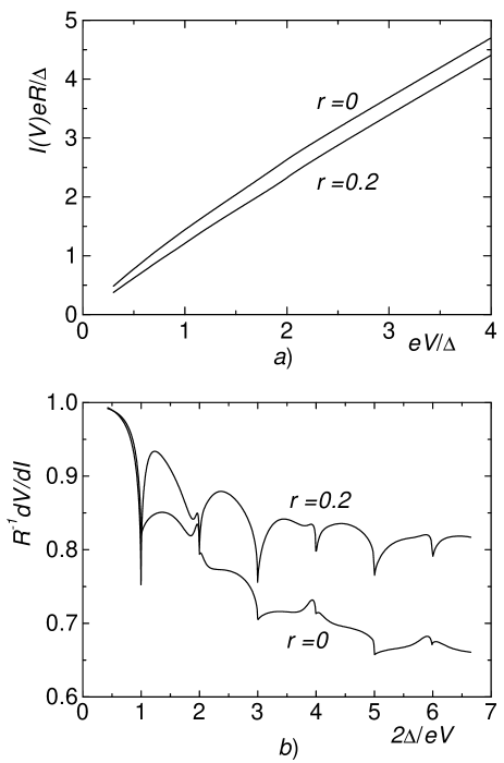
Similar to the case of low barrier transmittance, the current transport through an SNS junction with nearly perfect interfaces can be qualitatively explained within a simplified model of MAR, where the over-the-barrier () Andreev reflection is ignored. Indeed, as follows from Fig. 4, at , the tunnel resistances outside the gap are much smaller than the Andreev and/or normal resistances, except for a narrow region around the gap edges, where diverges due to complete Andreev reflection. This allows us to assume all the normal resistors at to be connected directly to the “voltage source” and therefore to exclude all Andreev resistors in Fig. 5 outside the gap. As a result, we arrive at the sequence of subcircuits shown in Fig. 6(c), with for side circuits. Thus, at , the subgap current may be approximately described by Eqs. (53), (57), with the tunnel and Andreev resistances renormalized by the proximity effect.
Within this model, the SGS oscillations in the differential resistance in Fig. 9 can be explained in the following way. As the voltage decreases, the subgap current, which approximately follows Ohm’s law, undergoes an additional suppression in the vicinity of the gap subharmonics, due to the presence of a high-resistive circuit with two large tunnel resistors located just at the gap edges. These current steps, being almost invisible in the - characteristic, manifest themselves as sharp dips in . At even subharmonics, this effect is partially compensated by the middle negative Andreev resistor, which rapidly reduces the effective normal metal resistance due to the increase in the size of the proximity region at small energies. As a result, the even dips become less pronounced and, as long as the interface transparency increases, turn into small peaks. At low voltages, the differential resistance approaches a constant value, which can be estimated for perfect NS interface by the following expression similar to Eq. (58):
| (84) | |||
| (85) |
Unlike the ballistic SNS junction,[1, 3] but similar to short diffusive constriction,[5] the SGS survives at zero temperature even for perfect NS interfaces. In this case, the SGS occurs due to coherent impurity scattering of quasiparticles inside the proximity region, with the amplitude approximately proportional to the characteristic length of this region. If we neglect the proximity corrections (), the SGS disappears, along with the excess current, and the - characteristic shows perfect Ohmic behavior.[7] Thus, we conclude that in the both cases of resistive and transparent NS interfaces, SGS appears due to the normal electron backscattering in the proximity region. This formally corresponds to the finite value of the renormalized Andreev resistance of the interface.
VIII Role of inelastic scattering
Since the relative SGS amplitude increases along with the NS barrier strength (though the current itself decreases), one might expect systems with high-resistive interfaces to be more favorable for the experimental observation of SGS. However, there exists an intrinsic restriction for the effect: to provide strong nonequilibrium of the subgap quasiparticles inherent to MAR, the time of their diffusion through the whole MAR staircase, from to , must be smaller than the inelastic relaxation time . The value of can be estimated as the time for diffusion over an effective length . At low interface resistance, , the diffusion rate is basically determined by the impurity scattering: . For high interface resistance, , the large Andreev resistance present bottleneck which renormalizes the diffusion coefficient in by a small factor . In this way, the level of nonequilibrium of the subgap quasiparticles is controlled by the parameter
| (86) |
which must be large enough to allow observation of at least a few subharmonics in , i.e., the condition determines the lower boundary for the barrier transparency. An analogous estimate for the inelastic parameter, with the barrier resistance substituting for the Andreev resistance in Eq. (86), was obtained in Ref. [7] for an SNINS structure with perfect NS interfaces. In this case, the tunnel barrier does not affect the Andreev reflection but produces renormalization of the diffusion coefficient, .
At , when , the normal channel may be considered as a reservoir with a certain effective temperature (depending on the details of inelastic scattering which are beyond our model approach), and the - curve becomes structureless. At small , the SNS junction behaves at two SN junctions connected in series through the equilibrium normal reservoir.
IX Summary
We have developed a consistent theory of incoherent MAR in long diffusive SNS junctions with arbitrary transparency of the SN interfaces. We formulated a circuit representation for the incoherent MAR, which may be considered as an extension of Nazarov’s circuit theory[11] to a system of voltage biased superconducting terminals connected by normal wires in the absence of supercurrent. We constructed an equivalent MAR network which includes a new resistive element, ”Andreev resistor”, which provides electron-hole conversion at the SN interfaces. Separate Kirchhoff rules are formulated for electron (hole) population numbers and diffusive flows. Within this approach, the electron and hole population numbers are considered as potential nodes connected through the tunnel and Andreev resistors with a distributed voltage source – the equilibrium Fermi reservoirs in the superconducting terminals.
The theory was applied to calculation of the - characteristics. The subgap current decreases step-wise with decreasing applied voltage in junctions with resistive interfaces, while in junctions with transparent interfaces an appreciable SGS appears only on the differential resistance. In all cases, exhibits sharp structures whose maximum slopes correspond to the gap subharmonics, . The amplitude and the shape of SGS oscillations strongly depend on the interface/normal-metal resistance ratio and reveal a noticeable parity effect: difference of the amplitudes of the even and odd structures. This effect is specific for diffusive junctions: it comes from the strongly enhanced probability of Andreev reflection at zero energy. Inelastic scattering results in smearing of the SGS, which disappears at small applied voltage.
Our theory of incoherent MAR is valid as soon as the applied voltage is much larger than the Thouless energy: in this case, one may neglect the overlap of the proximity regions near the NS interfaces. In the opposite case, , the problem of the low-energy part of the effective circuit should be considered more carefully, by taking into account the interference between the proximity regions. Aspects of this ac Josephson regime have been considered in Ref. [23] in terms of adiabatic oscillations of the quasiparticle spectrum and distribution functions, which produce nonequilibrium ac supercurrent.[24] Within our approach, this effect will introduce an effective boundary condition for the probability currents at small energy, which must be included into the circuit representation of MAR in energy space.
It is useful to discuss the effect of dephasing on MAR which has not been sufficiently investigated yet. In the present case of diffusive junction, the dephasing is modeled by an imaginary addition to the energy, . It is easy to see that this model leads to more pronounced SGS. Indeed, as it follows from Eq. (7), the effect of large dephasing rate is similar to the effect of an opaque interface barrier (the transmissivity parameter becomes effectively small). This is easily understood since the dephasing suppresses the anomalous Green’s function within the normal metal similar to the effect of the interface barrier. Thus, even for highly transmissive interfaces, the - curves for large become similar to the ones in the case of low-transparent interfaces (see Fig. 7), with deficit current and pronounced SGS. This conclusion is also supported by direct numerical calculation. It is of interest that the parity effect in SGS almost disappears due to the cutoff of the long-range proximity effect at small energies. In such case, the incoherent MAR regime persists at arbitrarily small voltages and our theory is valid until the quasiparticle relaxation will affect MAR regime as described in Sec. VIII.
Acknowledgements.
Support from NFR, KVA and NUTEK (Sweden), from NEDO (Japan), and from Fundamental Research Foundation of Ukraine is gratefully acknowledged.The analytical expressions for bare conductivities and proximity corrections can be obtained in the case of low-transparent NS interface, , by making use of a perturbative solution of Eq. (7):
| (87) |
| (89) | |||
| (92) |
| (93) | |||
| (94) |
where is the Heaviside function and is assumed for brevity to be positive. From Eq. (89), we obtain approximations for the tunnel and Andreev resistances:
| (96) |
| (97) | |||
| (98) |
In the vicinity of the gap edges, , and at small energies, , where in Eq. (87) diverges, the following approximate solutions of Eq. (7) have to be used instead of Eq. (87):
| (99) |
at , where is the solution of a cubic equation , and
| (100) |
at . The asymptotics of and near these “dangerous” points, are given by
| (102) |
| (103) |
| (104) |
at . At ,
| (105) |
For perfect SN interface, , the asymptotics of at and are given by Eqs. (104), (105) respectively, whereas diverges at the gap edge as . Several examples of these dependencies calculated numerically are presented in Fig. 2 (see discussion in Sec. IV).
REFERENCES
- [1] T. M. Klapwijk, G. E. Blonder, and M. Tinkham, Physica B+C 109-110, 1657 (1982).
- [2] M. Octavio, M. Tinkham, G. E. Blonder, and T. M. Klapwijk, Phys. Rev. B 27, 6739 (1983); K. Flensberg, J. Bindslev Hansen, and M. Octavio, ibid. 38, 8707 (1988).
- [3] G. B. Arnold, J. Low Temp. Phys. 68, 1 (1987); U. Gunsenheimer, and A. D. Zaikin, Phys. Rev. B 50, 6317 (1994).
- [4] E. N. Bratus’, V. S. Shumeiko, and G. Wendin, Phys. Rev. Lett. 74, 2110 (1995); D. Averin, and A. Bardas, ibid. 75, 1831 (1995); J. C. Cuevas, A. Martin-Rodero, and A. Levy Yeyati, Phys. Rev. B 54, 7366 (1996).
- [5] A. Bardas, and D. V. Averin, Phys. Rev. B 56, 8518 (1997); A. V. Zaitsev, and D. V. Averin, Phys. Rev. Lett. 80, 3602 (1998).
- [6] A. V. Zaitsev, JETP Lett. 51, 41 (1990); Physica C 185-189, 2539 (1991).
- [7] E. V. Bezuglyi, E. N. Bratus’, V. S. Shumeiko, and G. Wendin, Phys. Rev. Lett. 83, 2050 (1999).
- [8] A. F. Volkov, and T. M. Klapwijk, Phys. Lett. A 168, 217 (1992).
- [9] W. M. van Huffelen, T. M. Klapwijk, D. R. Heslinga, M. J. de Boer, and N. van der Post, Phys. Rev. B 47, 5170 (1993); M. Kuhlmann, U. Zimmerman, D. Dikin, S. Abens, K. Keck, and V. M. Dmitriev, Z. Phys. B 96, 13 (1994); U. Zimmerman, S. Abens, D. Dikin, K. Keck, and V. M. Dmitriev, ibid. 97, 59 (1995); R. Taboryski, T. Clausen, J. Bindslev Hansen, J. L. Skov, J. Kutchinsky, C. B. Sørensen, and P. E. Lindelof, Appl. Phys. Lett. 69, 656 (1996); J. Kutchinsky, J. Taboryski, C. B. Sørensen, A. Kristensen, P. E. Lindelof, J. Binslev Hansen, C. Schelde Jacobsen, and J. L. Skov, Phys. Rev. Lett., 78, 931 (1997); J. Kutchinsky, R. Taboryski, O. Kuhn, C. B. Sørensen, P. E. Lindelof, A. Kristensen, J. Bindslev Hansen, C. Schelde Jacobsen, and J. L. Skov, Phys. Rev. B 56, 2932 (1997); R. Taboryski, J. Kutchinsky, J. Bindslev Hansen, M. Wildt, C. B. Sørensen, and P. E. Lindelof, Superlattices Microstruct. 25, 829 (1999); A. Frydman, and R. C. Dynes, Phys. Rev. B 59, 8432 (1999); Z. D. Kvon, T. I. Baturina, R. A. Donaton, M. R. Baklanov, K. Maex, E. B. Olshanetsky, A. E. Plotnikov, and J. C. Portal, cond-mat/9907247 (unpublished).
- [10] G. Johansson, G. Wendin, K. N. Bratus’, and V. S. Shumeiko, Superlattices Microstruct. 25, 905 (1999).
- [11] Yu. V. Nazarov, Phys. Rev. Lett. 73, 1420 (1994); Superlattices Microstruct. 25, 1221 (1999).
- [12] A. I. Larkin, and Yu. N. Ovchinnikov, Sov. Phys. JETP 41, 960 (1975); 46, 155 (1977).
- [13] M. Yu. Kupriyanov, and V. F. Lukichev, Sov. Phys. JETP 67, 89 (1988).
- [14] G. E. Blonder, M. Tinkham, and T. M. Klapwijk, Phys. Rev. B 25, 4515 (1982).
- [15] C. J. Lambert, R. Raimondi, V. Sweeney, and A. F. Volkov, Phys. Rev. B 55, 6015 (1997).
- [16] A. D. Zaikin, and G. F. Zharkov, Sov. J. Low Temp. Phys 7, 375 (1981).
- [17] E. V. Bezuglyi, E. N. Bratus’, and V. P. Galaiko, Low Temp. Phys. 25, 167 (1999).
- [18] S. N. Artemenko, A. F. Volkov, and A. V. Zaitsev, Sov. Phys. JETP 49, 924 (1979).
- [19] Here we apply the term “Andreev resistance” (and further “Andreev conductance”) to denote particular values of (or ). This must be distinguished from the term “Andreev conductance” widely used in literature for physical conductance of the junction at the subgap applied voltages.
- [20] A. F. Volkov, A. V. Zaitsev, and T. M. Klapwijk, Physica C 210, 21 (1993).
- [21] In the terms of the circuit theory, this means that the “voltage drop” between the electron and hole nodes is directed against the probability current flowing through the Andreev resistor.
- [22] Yu. V. Nazarov, and T. H. Stoof, Phys. Rev. Lett. 76, 823 (1996); T. H. Stoof, and Yu. V. Nazarov, Phys. Rev. B 53, 14496 (1996); A. F. Volkov, N. Allsopp, and C. J. Lambert, J. Phys.: Cond. Matter 8, L45 (1996).
- [23] S. V. Lempitskii, Sov. Phys. JETP 58, 624 (1983); F. Zhou, and B. Spivak, JETP Lett., 65, 369 (1997); N. Argaman, Superlattices Microstruct. 25, 862 (1999).
- [24] K. W. Lehnert, N. Argaman, H.-R. Blank, K. C. Wong, S. J. Allen, E. L. Hu, and H. Kroemer, Phys. Rev. Lett. 82, 1265 (1999).