[
Experimental Evidence for Electron Channelling in Fe/Au (100) Multilayers
Abstract
We present transport and structural data from epitaxial (100) and (111) Au/Fe multilayers grown by molecular beam epitaxy. From their analysis, we conclude that an electron channelling mechanism, due to strong specular reflection of the minority spin carrier at the Au/Fe interfaces, is responsible for the high conductivity in the (100) multilayers.
pacs:
PACS numbers: 75.70.Pa, 75.70.-i, 73.40.-c]
The theory of the giant magnetoresistance (GMR) in magnetic multilayers is still developing [1, 2] and a number [3] of recent papers have interesting predictions about the nature of the electronic states in multilayers. In particular, the band structure that gives rise to spin-dependent scattering is thought to be responsible [4] for the spin-dependent confinement of electrons to specific layers within the system. A potential step can exist at the interface between the ferromagnetic layer and the non-magnetic layer. This potential in the hybridised band structure affects the transmission of electrons through the interface. It should be possible, therefore, for electrons to scatter specularly from such an interface, and theoretical work has predicted the effect on the transport[5, 6, 7, 8, 9, 10] and coupling properties in superlattices[11, 12, 13].
This type of specular reflection is quite distinct from that explored experimentally by Egelhoff et al[14], Swagten et al[15] and Yuasa et al[16] where electrons are specularly scattered from an insulator or noble metal/vacuum interface. In true channelling the electron is confined to a layer within the material as a result of the band structure. States are completely reflecting if there are no states in the other material with the same parallel momentum. Additionally, at points of high symmetry, the effectiveness of coupling between s-p states of the spacer and the d-states of the ferromagnet become important and lead to high reflection probabilities that are different for majority and minority carriers. When the magnetic moments in adjacent layers are parallel, one spin can have a high specular reflection coefficient at both interfaces and the spacer acts as an electron waveguide. If this spacer has a significantly lower resistivity than the magnetic layer, the channelled electrons will act as a low resistance shunt and thus enhance the GMR. In the antiparallel state, there is no confinement in the Au.
According to the theory of Stiles[7], the Fe/Au (100) system is a good candidate in which to observe electron channelling. The probabilities for transmission into the Fe from the Au are 67 higher for majority carriers compared to the minority carriers. For transmission from the Fe into the Au, the majority carriers have a 21 higher probability of transmission. On the other hand, the minority electrons are largely confined to each material. The orientation between the successive magnetic moments in a multilayer greatly affects the channelling. Only in the saturated state where all magnetic moments are aligned can the channelling occur. Also, the channelling is related to the symmetry of the Fermi surface and therefore to the epitaxial relationship in the superlattice. Large channelling effects are predicted for (100) Fe/Au whereas the Fe/Au(111) system is not expected to exhibit channelling as the band mis-match is so large[17].
In this letter, we present experimental evidence for this mechanism in (100) oriented Fe/Au multilayers grown by Molecular Beam Epitaxy (MBE)[18]. The key experiments involve the study of the variation of conductivity and structural perfection as a function of the thickness of the Au layers. Fe/Au multilayers consisting of 20 repeats of a [Fe(10Å)/Au(X)] structure, where X represents a thickness between 5 and 70 Å, were grown on a 50Å Au buffer layer. In-situ RHEED measurements and high resolution x-ray diffraction data from Bragg planes parallel to the surface showed that multilayers grown on polished (100) faces of MgO (with a 10Å Fe seed layer) were epitaxial with (100) orientation, while those grown on (110) sapphire (with a 30Å Nb seed layer) were (111) oriented. The existence of superlattice satellites up to the seventh order around the 200 and 111 x-ray Bragg peaks for the respective systems showed that the interfaces were extremely sharp. Analysis of the diffraction peak widths in reciprocal space scans of 30Å bilayer samples gives a lower limit to the out-of-plane sub-grain size of 150 20Å and 570 50Å in the (100) and (111) systems respectively. In these samples, for both orientations, there are many interfaces contained within each sub-grain. It is important for the transport data presented later, to note that we find the out-of-plane structure for the (111) samples to be of much higher quality than the (100) samples.
Oscillations, as a function of Au spacer thickness, in GMR (measured using a 4-probe DC method at 4.2K) and in the remanent magnetisation were observed in the (100) orientation only. Our measured values of 15 2Å and 7 2Å for the period of the exchange coupling compares well with predicted values of 17.2Å and 5.0Å[19] and those determined elsewhere[20, 21]. However, the decay length of the coupling strength, as a function of spacer, thickness was unusually long. Several theoretical papers have predicted that the amplitude of exchange coupling is a function of the extent of electron confinement[11, 12, 13]. There was no coupling observed in the (111) samples and a maximum GMR of only 6 was found compared to 40 for the (100) samples with antiferromagnetic coupling.
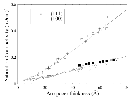
The conductivity at 4.2K, measured in a saturating magnetic field of 1T, as a function of Au spacer thickness is shown in Fig 1. The conductivity of a single bilayer of [Au(1000Å)/Fe(10Å)] has been measured as in the (100) orientation and in the (111) orientation. It is immediately apparent that the data from Fig 1 should saturate, for large Au thickness, at roughly the same value, i.e. the conductivity of thick Au. We have found that while the (111) data can be explained in the Fuchs-Sondheimer model[22], the (100) data cannot, for any reasonable values of the Fe or Au conductivities. If electrons were to traverse many layers without scattering, the conductivity would depend on the average scattering properties of many Au and Fe layers and would not vary strongly with the thickness of the Au(100) spacer. However, if electron channelling exists in the (100) Au spacers, the mean-free path of the specularly reflected electrons may be long, leading to a high conductivity, without electrons crossing a large number of layers. The number N, of specular reflections prior to diffusive scattering at the Fe/Au interface, is determined by the potential step at the interface and does not change with Au-thickness. Provided the mean free path in the Au layer, , is greater than the thickness of the Au, the mean free path is directly proportional to the product of the number of specular reflections and the Au thickness: . The total conductivity, , measured in-plane is then the thickness-weighted sum of the conductivities of the individual Fe and Au layers, namely,
| (1) |
where tAu and tFe are the thicknesses of Au and Fe layers, ttot is the total multilayer thickness, the conductivity of the Fe layers and represents the usual constants from the Drude formula. Solid lines in Fig. 1 represent fits using equation 1 assuming that is the same for all samples, independent of Au thickness and multilayer orientation. The only free parameter is the value of N and we find that the ratio of specular reflection coefficients between orientations, N100 / N111 is 2.7 0.1 with N100 equal to 9.
To go beyond this phenomenological model which assumes a spin independent electron confinement, we have used the semi- classical model proposed by Hood and Falicov[4] to determine the saturation conductivity in an infinite [Fe(10Å)/Au(XÅ)] multilayer as function of X. We have calculated the conductivity with and without specular reflections assuming spin dependent scattering probabilities in the bulk and at the interfaces. The spin dependent relaxation time and potential of the layer were varied to keep the conductivity equal to that measured in the bulk. At the interface, three possible cases are distinguished: transmision (T), specular reflection (R) and diffuse scattering (D) where T+R+D=1. The values of T and R are determined by the layer potentials and D was set as 0.3 for all layers. We have set the potential of the Au layer in agreement with the free electron value of the Fermi energy. In order to confine the electrons, the potential in the Fe must be varied. As expected, free electron values of the Fermi energy for Fe do not work and therefore, to introduce confinement in the Au, the potentials for majority and minority carriers in Fe are changed.
Within the model we find that without electron confinement the (100) Au conductivity must be 25 times higher than the (111) Au to explain the experimental data. This is unreasonable considering the structural data and the measured conductivities. We therefore fixed the conductivities of layers in each orientation to be equal to the measured values and then switched on the channelling for the (100) samples. The results are shown as squares in Fig 1. The agreement with the experimental data is very good when the probability of specular reflection is set to 0.6 for minority electrons and 0.3 for the majority electrons, which is close to the values predicted by Stiles [7]. We also found that varying D, the diffuse scatter at the interface, could not account for the data. We conclude therefore, that channelling is required to explain the observed differences in the conductivity of (100) and (111) superlattices.
We have undertaken extensive structural measurements to demonstrate the validity of the above analysis which assumes no significant change in the structural quality of the samples with Au thickness. In-plane diffraction measurements have been carried in-situ using Reflection High Energy Electron Diffraction (RHEED) and ex- situ using Grazing Incidence X-Ray Diffraction (GIXD). To perform an in-situ RHEED analysis, the growth of an 80Å Au layer on 10Å of Fe has been interrupted at different stages. The patterns exhibit fine and continuous streaks characteristic of a 2-D well ordered Au-surface, which is expected from the difference of free surface energy of the materials. The full width at half maximum (FWHM) of the streaks is a measure of the in-plane coherence length. As can be seen in Fig 2, this was found to be constant in both of the orientations for Au layers thicker than 30Å, where the conductivity in Fig 1 shows significant dependence on the Au thickness. For thick Au, the coherence length of the (111) samples was slightly larger than the (100).

Grazing incidence x-ray diffraction experiments have been performed on BM28, the XMaS CRG beamline, at the European Synchrotron Radiation Facility in Grenoble. In the GIXD geometry, the diffracting planes are perpendicular to the sample surface and the diffraction peaks measured by rotation of sample and detector about the normal to the surface. It is therefore sensitive to in-plane structure and disorder in the Au and Fe layers. Use of a grazing angle of the incident beam below the critical angle, (in our experiments 0.2∘), limits the depth sensitivity to approximately 30Å. The FWHM of the in plane -2 scans are 0.8 for the (111) and 0.2 for the (100) orientation samples respectively. Figure 3 shows scans of scattered intensity as a function of the specimen angle about its surface normal taken with the detector at the Au (022) reflection position. The 4- and 6-fold symmetries show the Au layers to be deposited with well-defined (100) and (111) orientation in the MgO and sapphire systems respectively. The FWHM of the peaks of Fig 3 provides a direct measure of the mosaic width of in-plane crystalline disorder. For the (100) samples, the mosaicity width was found to vary from 0.49∘ to 0.47∘ for Au layer thicknesses between 35Å and 70Å whereas for (111) the widths varied from 2.35∘ to 2.02∘. The absence of variation of rocking curve FWHM with thickness in the (100) samples is strong evidence against defect scattering being responsible for the change in the conductivity[28].

The specular reflectivity data show Kiessig fringes and Bragg peaks for both (100) and (111) epilayers, and the nominal thickness was found to be in good agreeement with that deduced from the x-ray results. Kiessig fringes and Bragg peaks were also observed in the off-specular radial scans, indicating that a large proportion of the interface roughness is correlated (conformal) through the multilayer. The thickness of individual layers, the electron density gradient, conformal and random roughness, in-plane correlation length () and Hirst fractal parameter, h, were obtained by matching the experimental data to that simulated for a fractal model structure within the Distorted Wave Born Approximation[23, 24]. Excellent agreement is found between experimental and simulated data for transverse (qy) scans, with good reproducibility between samples. For the (111) Fe/Au epilayers grown on sapphire we find (Fig. 4a) that the interface roughness is highly correlated in nature with a correlated-to-uncorrelated roughness ratio close to 16:1. The lateral correlation length, , is determined to be 250 20Å with a fractal Hirst parameter h=0.20 0.05. The (100) Fe/Au grown on MgO also exhibits an interface roughness which is highly correlated in nature. Matching of simulated and experimental data (Fig. 4b) yields a correlated-to-uncorrelated roughness ratio of 10:1 and a lateral correlation length =250 20Å, with a fractal parameter h=0.28 0.05. In all layers measured, the r.m.s. amplitude of the roughness in the (100) system is almost three times that of the (111) system, (9.3 0.2Å compared with 3.3 0.2Å). The interface morphology is found to stay the same when varying the Au thickness. Therefore, these structural properties imply that the (111) system should have the higher conductivity, contrary to the observations.

The values of , determined from the intercept in Fig 1, are very similar in the (111) and (100) materials. GIXD measurements indicate that the (100) Fe is in good crystallographic registration with the (100) Au as expected from the lattice matching. In-situ RHEED data[25] and ex situ Medium Energy Ion Scattering[26] experiments from multilayers grown on sapphire showed that the growth of Fe (111) on Au(111) is pseudomorphic for Fe thicknesses less than 10Å in agreement with previous results [27]. The (111) Fe/Au system eventually relaxes into its bulk structure, but only after the Fe thickness becomes greater than 15Å. For all samples in this study, therefore, both orientations grow epitaxially.
The structural studies show that neither the variation of the saturation conductivity as a function of Au layer thickness nor the difference between (100) and (111) oriented multilayers can be attributed simply to the difference in sample quality. We thus conclude that the data in Fig 1 demonstrate the existence of electron channelling in Fe/Au (100) multilayers.
Acknowledgements: We would like to thank M. Horlacher for coding the Hood and Falicov model, J. Xu for some of the resistivity measurements for the (111) samples, M. A. Howson and W. P. Pratt for valuable discussions. The helpful and friendly assistance at the ESRF of T.P.A Hase and XMaS beam line members S.D. Brown, D.F. Paul, A. Stunault and P. Thompson and financial support from the Engineering and Physical Science Research Council is gratefully acknowledged.
REFERENCES
- [1] Bozec, D., Howson, M.A., Hickey, B.J., et al. accepted for publication in Phys Rev Lett.
- [2] Brataas A, Nazarov Yu V, Bauer GEW, Phys Rev Lett 84 2481 (2000).
- [3] Butler WH, Zhang XG, MacLaren JM, J Supercond. 13, 221 (2000). Schulthess TC, Butler WH, Zhang XG, et al. Phys Rev 56, 8970 (1997). Zhang XG, Butler WH, Phys Rev B 51, 10085 (1995). Tsymbal EY and Pettifor DG, Phys Rev B 61, 506 (2000). Tsymbal EY and Pettifor DG J Magn Magn Mater 202, 163 (1999). Tsymbal EY, Pettifor DG, Phys Rev B 54, 15314 (1996). Sanvito S, Lambert CJ, Jefferson JH, Phys Rev B 60, 7385 (1999).
- [4] Hood, R.Q. and Falicov, L.M, Phys. Rev. B 46, 8287 (1992).
- [5] Butler WH, Zhang XG, et al. Phys Rev Lett 76, 3216 (1996).
- [6] Zhang, S. and Levy, P.M., Phys. Rev. B 57, 5336 (1998).
- [7] Stiles,M.D., J. Appl. Phys. 79, 5805 (1996).
- [8] Vedyayev, A., Cowache, C., Ryzhanova, N., Dieny, B., J. Phys. Condens. Matter 5, 8289 (1993).
- [9] Bulka, B.R. and Barnas, J.,Phys. Rev.B 51, 6348 (1995).
- [10] Schep, K.M. et al., J. Magn. Magn. Mater. 177, 1166, (1998).
- [11] Mathon, J., et al, J. Magn. Magn. Mater. 121, 242, (1993).
- [12] Stiles, M.D., Phys. Rev. B 48, 7238 (1993).
- [13] Bruno, P., Phys. Rev. B 52, 411 (1995).
- [14] Egelhoff, W.F., Chen, P.J., Powell, C.J., et al., J. Vac. Sci. Technol B 17, 1702 (1999). Egelhoff WF, Chen PJ, Powell CJ, et al. IEEE Trans Mag 33 3580 (1997).
- [15] Swagten, H.J.M., Strijkers, G.J., Bloemen, P.J.H., Willekens, M.M.H. and Dejonge, W.J.M.: Phys Rev. B 53, 9108 (1996).
- [16] Yuasa S, Katayama T, Nyvlt M, Suzuki Y and Yori T, J. Appl. Phys. 83, 7031 (1998).
- [17] Stiles, M.D., private communication.
- [18] Howson, M.A., Hickey, B.J., Garfield, J., et al., J. Phys. Condens. Matter. 11 5717 (1999). Xu, J., Howson, M.A., Hucknall, P., et al., J Appl. Phys. 81 3908 (1997).
- [19] Bruno, P. and Chappert, C.: Phys Rev Lett 67, 1602 (1991).
- [20] Shintaku, K., Daitoh, Y. and Shinjo, T.: Phys. Rev. B 47, 14584 (1993).
- [21] Unguris,J., Celotta, R.J. and Pierce, D.T.: J. Appl. Phys. 75, 6437 (1994).
- [22] See Thin Film Phenomena by K.L. Chopra McGraw-Hill London (1969).
- [23] Hase, T.P.A., Pape, I., Wormington, M. and Tanner, B.K.: Physica B 253, p278 (1998).
- [24] Sinha, S., Sirota, E.B., Garof, S., Stanley, H.B., Phys. Rev. B 38, 2297 (1988).
- [25] Dekadjevi, D.T., et al, to be published.
- [26] Noakes, T.C.Q , Bailey, P., Hucknall, P. K., Donovan, K., Howson, M. A., Phys. Rev. B 58, 4934 (1998).
- [27] Stroscio, J. A., Pierce, D. T., Dragoset, R. A., First, P. N., J. Vac. Sci. Tecnol. A. 10, 1981 (1992).
- [28] Modak, A.R., Smith, D.J., Parkin, S.S.P., Phys. Rev. B 50, 4232 (1994).