Localization length and impurity dielectric
susceptibility
in the critical regime
of the metal-insulator transition
in homogeneously doped -type Ge
Abstract
We have determined the localization length and the impurity dielectric susceptibility as a function of Ga acceptor concentrations () in nominally uncompensated 70Ge:Ga just below the critical concentration () for the metal-insulator transition. Both and diverge at according to the functions and , respectively, with and for . Outside of this region (), the values of the exponents drop to and . The effect of the small amount of compensating dopants that are present in our nominally uncompensated samples, may be responsible for the change of the critical exponents at .
pacs:
PACS numbers: 71.30.+h, 72.80.CwThe metal-insulator transition (MIT) in doped semiconductors is a unique quantum phase transition in the sense that both disorder and electron-electron interaction play a key role. [1] Important information about the MIT is provided by the values of the critical exponents for the zero-temperature conductivity, correlation length, localization length, and impurity dielectric susceptibility. From a theoretical point of view, the correlation length in the metallic phase and the localization length in the insulating phase diverge at the critical point with the same exponent , i.e., they are proportional to in the critical regime of the MIT. ( is the dopant concentration and is the critical concentration for the MIT.) Since direct experimental determination of is extremely difficult, researchers have usually determined, instead of , the value of defined by where is the conductivity extrapolated to . [2, 3] It is also possible to evaluate from finite-temperature scaling of the form where is equivalent to . [4, 5, 6] Values of are then obtained assuming for three-dimensional systems. [7]
In this work we have determined directly the localization length and the impurity dielectric susceptibility in neutron-transmutation-doped (NTD), nominally uncompensated 70Ge:Ga just below . The application of NTD to isotopically enriched 70Ge leads to unsurpassed doping homogeneity and precisely controlled doping concentration. As a result, we have been able to approach the transition as close as from the insulating side and from the metallic side. [3] In zero magnetic field, the low-temperature resistivity of the samples is described by variable-range hopping (VRH) conduction within the Coulomb gap. [8] Magnetic field and temperature dependence of the resistivity are subsequently measured in order to determine directly and in the context of the VRH theory. [8]
This kind of determination of and was performed for compensated Ge:As by Ionov et al. [9] They found and with and , respectively, for . The significance of their result is the experimental verification of the relation that had been predicted by scaling theories. [10, 11] However, the critical exponents of compensated samples are known to be different from those of nominally uncompensated samples. Therefore, the present work which probes and in nominally uncompensated samples is relevant for the fundamental understanding of the MIT. The previous effort to measure has also contributed. [12, 13, 14] Hess et al. found in nominally uncompensated Si:P. [13] Since was determined for the same series of Si:P samples, was again valid. Katsumoto has found and for compensated AlxGa1-xAs:Si, i.e., again, applies. [14] Thus, in these cases the conclusion was reached indirectly, by assuming . The work reported here, on the other hand, determines directly, i.e., we do not have to rely on the assumption in order to study the behavior of near .
All of the 70Ge:Ga samples used in this study were prepared by NTD of isotopically enriched 70Ge single crystals. We use the NTD process since it is known to produce the most homogeneous dopant distribution. [2] Details of the sample preparation and characterization are described elsewhere. [3] In this study, we determined the low-temperature ( K) resistivity of nine samples in weak magnetic fields ( T) applied in the direction perpendicular to the current flow.
The electrical conduction of doped semiconductors on the insulating side of the MIT is often dominated by VRH at low temperatures. The temperature dependence of the resistivity for VRH is written in the form of
| (1) |
where for the excitation within a parabolic-shaped energy gap (the Coulomb gap), [8] and for a constant density of states around the Fermi level. [15] In our earlier work, [3] we reported that for ( cm-3) and that decreases rapidly as approaches from and becomes even smaller than 1/4 when we neglect the temperature variation of . However, the variation contributes greatly to the temperature dependence of near because the factor in the exponential terms become very small, i.e., the temperature dependencies of and that of the exponential term become comparable. Theoretically, is expected to vary as but the value of including the sign has not been derived yet for VRH with both (Ref. REFERENCES) and (Ref. REFERENCES).
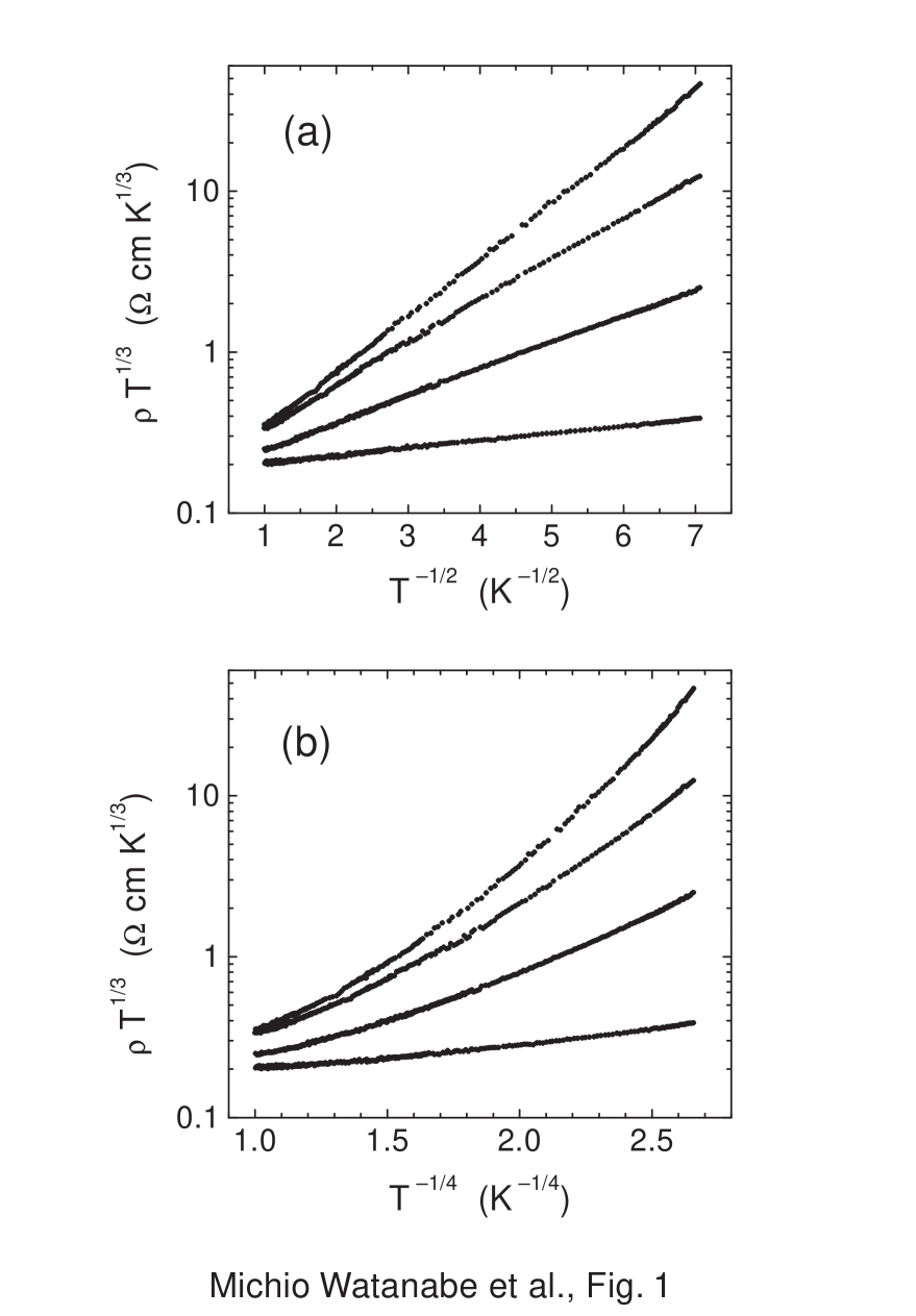
Recently, we have shown that the temperature dependence of the conductivity of the same series of 70Ge:Ga samples within 0.3% of is proportional to at K. [3] Since both the dependence of the conductivity and the Efros-Shklovskii VRH are results of the electron-electron interaction in disordered systems, they can be expressed, in principle, in a unified form. Moreover, the electronic transport in barely metallic samples and that in barely insulating samples should be essentially the same at high temperatures so long as the inelastic scattering length and the thermal diffusion length are smaller than, or at most comparable to the correlation length or the localization length. So, the temperature dependence of conductivity at high temperatures should be the same on both sides of the transition. Such behavior is confirmed experimentally in the present system, [3] i.e., the conductivity of samples very close to shows a dependence at K, irrespective of the phase (metal or insulator) to which they belong at . Based on this consideration we fix . Figure 1 shows with for four samples (, 0.994, 0.996, and 0.998) as a function of (a) and (b) . All the data points lie on straight lines with in Fig. 1(a) while they curve upward with in Fig. 1(b). This dependence is maintained even when we change the values of between 1/2 and 1/4. Thus we conclude that the resistivity of all samples for up to 0.998 is described by the VRH theory where the excitation occurs within the Coulomb gap, i.e., Eq. (1) with .
Based on these findings, we evaluate in Eq. (1) with and , and show it as a function of in Fig. 2. The vertical and horizontal error bars have been estimated based on the values of obtained with and , and the values of cm and cm, where cm-3 is the highest concentration in the insulating phase and cm-3 is the lowest in the metallic phase, respectively.
According to theory, [8] in Eq. (1) is given by
| (2) |
in SI units, where is the dielectric constant. Here, we should note that the condition is needed for the theory to be valid, i.e., has to be evaluated only from the data obtained at temperatures low enough to satisfy the condition. This requirement is fulfilled in Fig. 2 for all the samples except for the one with . Concerning this latter sample, we will include it for the determination of and (Fig. 5) but not for the calculation of the critical exponents.
Our next step is to separate into and . For , the magnetoresistance is expressed as
| (3) |
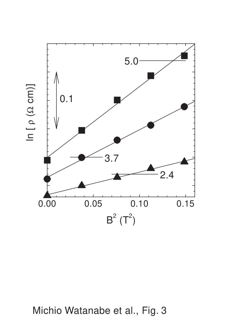
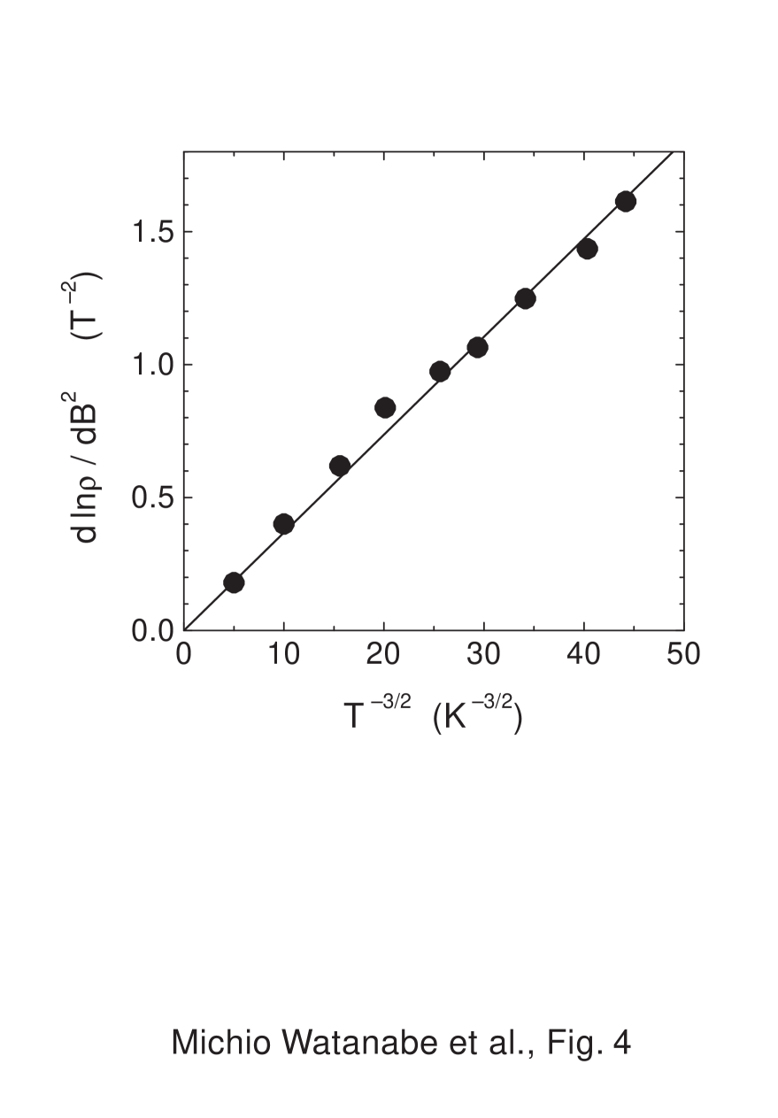
where is the magnetic length in SI units. [8] According to Eq. (3), the magnetic-field variation of at is proportional to , i.e., , and the slope is proportional to . In order to demonstrate that these relations hold for our samples, we show for the sample vs in Fig. 3 and determined by least-square fitting of vs in Fig. 4. Since Eq. (3) is equivalent to
| (4) |
is given by
| (5) |
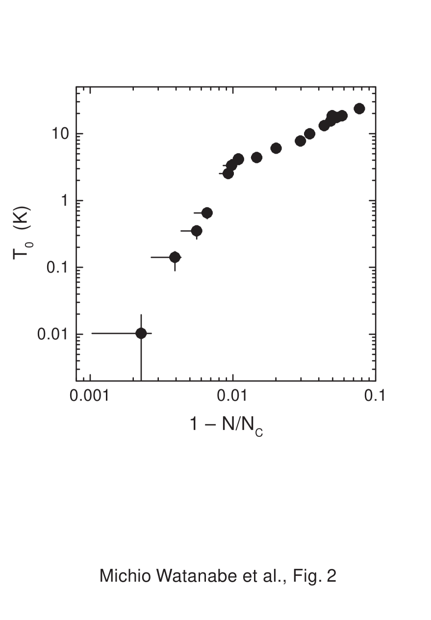
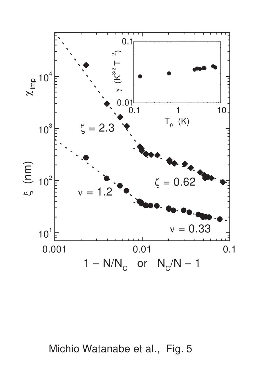
In this way we have determined for nine samples. The inset of Fig. 5 shows as a function of . The value of is almost independent of , and if one assumes , one obtains a small value of from least-square fitting. Figure 5 shows and determined from Eqs. (2) and (5). Here, is the dielectric constant of the host Ge, and hence, is the dielectric susceptibility of the Ga acceptors. We should note that both and are sufficiently larger than the Bohr radius (8 nm for Ge) and (Ref. REFERENCES), respectively. According to the theories of the MIT, both and diverge at as and , respectively. We find, however, both and do not show such simple dependencies on in the range shown in Fig. 5, and that there is a sharp change of both dependencies at . On both sides of the change in slope, the concentration dependence of and are expressed well by the scaling formula as shown in Fig. 5. Theoretically, the quantities should show the critical behavior when is very close to . So and may be concluded from the data in . However, the other region (), where we obtain and , is also very close to in a conventional experimental sense.
As a possible origin for the change in slope, we refer to the effect of compensation. Although our samples are nominally uncompensated, doping compensation of less than 0.1% may present due to residual isotopes that become -type impurities after NTD. In addition to the doping compensation, the effect known as “self compensation” may play an important role near . [18] It is empirically known that the doping compensation affects the value of the critical exponents. Rentzsch et al. studied VRH conduction of n-type Ge in the concentration range of , and showed that vanishes as with for % and 54%, where is the compensation ratio. [19] Since [Eq. (2)], we find for our 70Ge:Ga samples for and for . Interestingly, agrees with found for compensated samples. Moreover, we have recently proposed the possibility that the conductivity critical exponent in the same 70Ge:Ga only within the very vicinity of (up to about +0.1% of ). [6] An exponent of , on the other hand, holds for a wide region of up to . [3] Again, near may be viewed as the effect of compensation. Therefore, it may be possible that the region of around where and changes its width as a function of the doping compensation. In the limit of zero compensation, the part which is characterized by and vanishes, i.e., we propose , , and for truly uncompensated systems and that Wegner’s scaling law of is not satisfied. In compensated systems, on the other hand, Wegner’s law may hold as it does in the very vicinity of . The experiment on compensated AlxGa1-xAs:Si that showed and (Ref. REFERENCES) is also consistent with the law. However, our preceding discussion needs to be proven in the future by experiments in samples with precisely and systematically controlled compensation ratios.
In summary, we have determined directly the localization length and the dielectric susceptibility arising from the impurities in nominally uncompensated NTD 70Ge:Ga samples near the critical point for the MIT. While the relation predicted by scaling theory [10, 11] holds for , the critical exponents for localization length and impurity susceptibility change at . The small amount of doping compensation that is unavoidably present in our samples may be responsible for such a change in the exponents.
We are thankful to T. Ohtsuki, B. I. Shklovskii, and M. P. Sarachik for valuable comments, and V. I. Ozhogin for the supply of the Ge isotope. Most of the low-temperature measurements were carried out at the Cryogenic Center, the University of Tokyo. M. W. would like to thank the Japan Society for the Promotion of Science (JSPS) for financial support. The work at Keio was supported by a Grant-in-Aid for Scientific Research from the Ministry of Education, Science, Sports, and Culture, Japan. The work at Berkeley was supported by the Director, Office of Energy Research, Office of Basic Energy Science, Materials Sciences Division of the U. S. Department of Energy under Contract No. DE-AC03-76SF00098 and U. S. NSF Grant No. DMR-97 32707.
REFERENCES
- [1] P. A. Lee and T. V. Ramakrishnan, Rev. Mod. Phys. 57, 287 (1985); D. Belitz and T. R. Kirkpatrick, ibid. 66, 261 (1994).
- [2] K. M. Itoh et al., Phys. Rev. Lett 77, 4058 (1996).
- [3] M. Watanabe et al., Phys. Rev. B 58, 9851 (1998).
- [4] S. Bogdanovich, M. P. Sarachik, and R. N. Bhatt, Phys. Rev. Lett. 82, 137 (1999).
- [5] S. Waffenschmidt, C. Pfleiderer, and H. v. Löhneysen, Phys. Rev. Lett. 83, 3005 (1999).
- [6] K. M. Itoh et al., Ann. Phys. (Leipzig) 8, 631 (1999).
- [7] F. J. Wegner, Z. Phys. B 25, 327 (1976).
- [8] B. I. Shklovskii and A. L. Efros, Electronic Properties of Doped Semiconductors (Springer-Verlag, Berlin, 1984).
- [9] A. N. Ionov, I. S. Shlimak, and M. N. Matveev, Solid State Commun. 47, 763 (1983).
- [10] A. Kawabata, J. Phys. Soc. Jpn. 53, 318 (1984).
- [11] Y. Imry, Y. Gefen, and D. J. Bergman, in Anderson Localization, Proceedings of the Fourth Taniguchi International Symposium, Sanda-Shi, Japan, 1981, edited by Y. Nagaoka and H. Fukuyama (Springer-Verlag, Heidelberg, 1982), p. 15.
- [12] T. G. Castner, Philos. Mag. B 42, 873 (1980).
- [13] H. F. Hess et al., Phys. Rev. B 25, 5578 (1982).
- [14] S. Katsumoto, in Localization and Confinement of Electrons in Semiconductors, edited by F. Kuchar, H. Heinrich, and G. Bauer (Springer-Verlag, Berlin, 1990), p. 117.
- [15] N. F. Mott, Metal-Insulator Transitions, 2nd ed. (Taylor & Francis, London, 1990).
- [16] B. I. Shklovskii (private communication).
- [17] See, for example, Sec. 4 in F. R. Allen and C. J. Adkins, Philos. Mag. 26, 1027 (1972).
- [18] R. N. Bhatt and T. M. Rice, Philos. Mag. B, 42, 859 (1980).
- [19] R. Rentzsch et al., Phys. Status Solidi B 205, 269 (1998).