[
Bias and temperature dependence of the 0.7 conductance anomaly in Quantum Point Contacts
Abstract
The 0.7 conductance anomaly is studied in strongly confined, etched GaAs/GaAlAs quantum point contacts, by measuring the differential conductance as a function of source-drain and gate bias as well as a function of temperature. We investigate in detail how, for a given gate voltage, the differential conductance depends on the finite bias voltage and find a so-called self-gating effect, which we correct for. The 0.7 anomaly at zero bias is found to evolve smoothly into a conductance plateau at 0.85 at finite bias. Varying the gate voltage the transition between the 1.0 and the 0.85 plateaus occurs for definite bias voltages, which defines a gate voltage dependent energy difference . This energy difference is compared with the activation temperature extracted from the experimentally observed activated behavior of the 0.7 anomaly at low bias. We find which lends support to the idea that the conductance anomaly is due to transmission through two conduction channels, of which the one with its subband edge below the chemical potential becomes thermally depopulated as the temperature is increased.
pacs:
PACS 73.61.-r, 73.23.-b]
I Introduction
The quantized conductance through a narrow quantum point contact (QPC), discovered in 1988[1, 2], is one of the key effects in mesoscopic physics. The quantization of the conductance in units of the spin degenerate conductance quantum, , can be explained within a single-particle Fermi-liquid picture in terms of the Landauer-Büttiker formalism as, in the most simple case, adiabatic transport through the constriction. For a review see Ref. [3].
Since 1995 several experiments [4, 5, 6, 7] on quantum wires and point contacts have revealed deviations from this integer quantization, . In particular the 0.7 conductance anomaly, noted for the first time in 1991[8] but first studied in detail in 1996[7], poses one of the most intriguing and challenging puzzles in the field both experimentally and theoretically [9, 10, 11, 12, 13, 14, 15, 16, 17]. This anomaly is a narrow plateau, or in some cases just a shoulder-like feature, clearly visible at the low density side of the first conductance plateau in the dependence of the conductance on a gate voltage which tunes the width and the electron density of the QPC. For low bias voltage the conductance value of the anomalous plateau is around giving rise to the name of the phenomenon. The 0.7 anomaly has been recorded in many QPC transport experiments involving different materials, geometries and measurement techniques.
In this paper, we present experimental evidence, that the 0.7 conductance anomaly is associated with a density-dependent energy difference separating two transmission channels. We reach this conclusion by measuring both the temperature and the source-drain bias voltage dependence of the differential conductance, , through shallow-etched QPCs.
The outline of the paper is as follows. In Sec. II we describe the fabrication of the six samples to be investigated. In the following all detailed results on the conductance of the QPCs are shown solely for sample A, and only towards the end of the paper the main results from all samples are shown. In Sec. III we discuss the lateral confinement potential defining the QPC, and we focus in particular on the fact that this potential is controlled by two independent variables: the gate bias and the source-drain bias. Then follows in Sec. IV the results from finite source-drain bias spectroscopy, and the important energy difference is introduced. We deal with the temperature dependence of the zero-bias conductance in Sec. V and introduce the activation energy . The main result is obtained in Sec. VI where we show that for all six samples. A short conclusion is given in Sec. VII.
II The shallow etched samples
The quantum point contacts were all fabricated on modulation doped GaAs/GaAlAs heterostructures grown by molecular beam epitaxy (MBE). The layer sequence is: 1 m buffer, spacer, barrier layer with a Si concentration of m-3, and a 10 nm undoped GaAs cap layer. The carrier density is m-2 and the mobility is 100 m2/Vs, measured in the dark at a temperature of 4.2 K.
The samples were processed with a (m)2 mesa, etched 100 nm, and AuGeNi ohmic contacts to the 2DEG were formed by conventional UV-lithography, lift-off and annealing. The narrow QPC constriction was defined using electron beam lithography (EBL) and shallow wet-etching on the mesa. The following procedure was used: The sample was flushed in acetone, methanol and iso-propanol before it was ashed in an oxygen plasma for 20 seconds. The sample was then pre-etched in 18% HCl for 5 minutes, flushed in H2O and blown dry in nitrogen. It was then pre-baked for 5 minutes at 185 ∘C before spinning on a 125 nm thick layer of PMMA electron beam resist. The EBL pattern was exposed with an acceleration voltage of 30 kV, and developed in MIBK:iso-propanol (1:3). The sample was post-baked for 5 minutes at 115 ∘C, and ashed 6 seconds before etching 55-60 nm in at an etch rate of 100 nm/min.
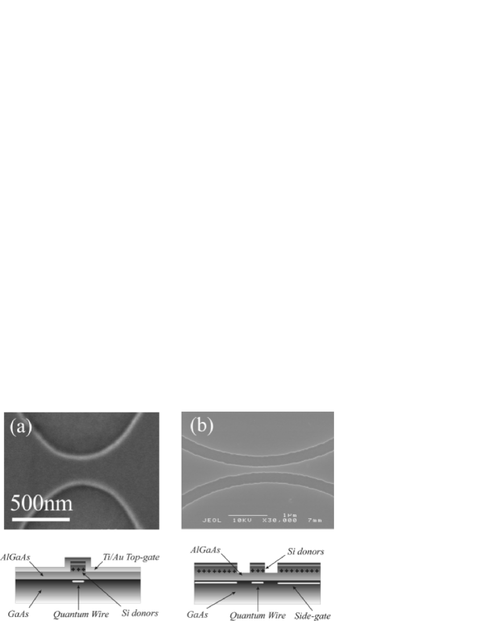
Three types of devices were investigated: top-gated (type I), side-gated (type II), and overgrown side-gated (type III). Fig. 1a shows a scanning electron microscope (SEM) picture of a type I QPC constriction. The shallow etched walls of the constriction are shaped as two back-to back parabolas. The picture was taken before the constriction was covered by a 10 m wide, 100 nm thick Ti/Au top-gate electrode. In type II devices, Fig. 1b, the QPC constriction is formed by etching two semi-circular trenches, 250 nm wide and 60 nm deep. The etched trenches also define two large areas of 2DEG which are used as side-gates. The same pattern is used in type III devices, but the trenches are etched 90 nm deep to reach the GaAs/GaAlAs interface and then MBE-regrown. In this way the constriction is bounded by heterostructure-interfaces, both vertically and laterally. The e-beam patterning and the MBE-regrowth was made before the Ohmic contacts were deposited. Before the regrowth, the sample was desorbed at C for 2 minutes in the MBE-chamber. The sample was then overgrown with 100 nm undoped and a 5 nm undoped GaAs cap layer, using a growth temperature of C. The sample parameters are tabulated in Table I.
The samples were mounted in a liquid helium refrigerator, and the differential conductance, , was measured with a small ac excitation voltage, 5-50 V rms, using standard lock-in techniques at 33-117 Hz. The effective width of the QPC and the electron density inside it is controlled by a gate voltage, which is applied between the source contact and the top or side gate electrode. Henceforth this gate voltage is denoted .
| Sample | A | B | C | D | E | F |
|---|---|---|---|---|---|---|
| type | I | II | II | II | III | III |
| width (nm) | 200 | 150 | 140 | 110 | 100 | 100 |
| radius (m) | 0.1 | 2 | 5 | 10 | 2 | 2 |
| (meV) | 6.5 | 7.5 | 9.7 | 10.0 | 5.7 | 5.9 |
III The lateral confinement
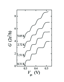
The shallow etching technique gives rise to a strong lateral confinement in the constriction. We have previously reported observation of quantized conductance at temperatures above 30 K in a 50 nm wide shallow etched QPC with a 1D-subband energy separation meV [11]. In this paper our main example is sample A (type I), but all the measurements reported for this sample have also been performed for the others. Fig. 2 shows the gate-characteristics, i.e. the differential conductance, , as function of gate-source voltage, , of sample A, measured at different temperatures. The 200 nm wide, etched QPC constriction is depleted at zero gate-voltage, and a positive gate-source voltage is necessary to open it. We estimate the 1D-subband energy separations in the QPC’s from the thermal smearing of the conductance plateaus, and more precisely by finite bias spectroscopy as described below. For the 200 nm wide QPC constriction in device A we find an energy separation between the two lowest 1D-subbands, meV, see also Table I and Sec. IV B.
The confinement potential determines the transmission properties of the device. It is mainly defined by the sample parameters, the geometry, and the gate-source voltage . However, to some extend, especially near pinch-off where the electron density is low, it does also depend on the bias voltage [19]. In short we write . This effect of influencing we denote ’self-gating’ since it resembles the ordinary gate effect from [20]. A sample exhibiting a self-gating can be said to be ’soft’, if not it is ’rigid’.
The current through the QPC can be expressed in terms of the transmission functions and the difference in thermal occupation factors for the source and drain reservoirs as:
| (1) |
where
| (2) | |||||
| (3) |
with being a number between 0 and 1 describing the ratio of the potential drop on each side of the constriction. Our experimental results are compatible with . Writing explicitly the most relevant functional dependencies for the current we obtain:
| (4) |
From this follows to first order in a Taylor expansion the expressions for the differential conductance and the transconductance , the quantities measured in the experiments:
| (5) | |||||
| (6) |
We note that any sharp features in the transconductance reminiscent of the characteristic step-like form in the conductance (see Fig. 2) derives from the factor in Eq. (6) relating to the opening of new conductance channels. The other factor is just varying smoothly due to its origin in electrostatics over length scales of the order of at least 100 nm. But also appears as a prefactor in the first term of the differential conductance in Eq. (5). Thus the self-gating effect is enhanced when the transconductance is large. Conversely, at low temperatures at the middle of a plateau the current is almost unaffected by changes in , at least only very smooth changes are expected. If can be neglected, the differential conductance is given by the occupation factor related second term in Eq. (5). As the temperature is enhanced the transconductance becomes more important even at the center of the plateau as is evident for the highest temperatures in Fig. 7.
IV Bias spectroscopy and the energy difference
An important source of information about the energy subbands in a QPC is finite bias spectroscopy. We use the technique developed by Patel et al. [8] and described theoretically by Glazman and Khaetskii[21]. The differential conductance, , at finite dc source-drain bias voltage, is measured by lock-in technique, using a small ac signal, 50 V rms 117 Hz, superposed on the dc source-drain bias voltage.
A The differential conductance at finite bias
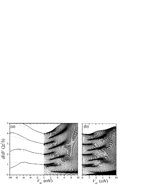
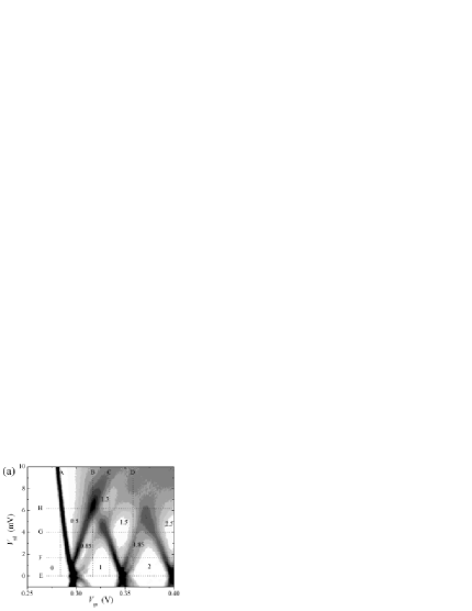
In Fig. 3 it is shown how at K the differential conductance of sample depends on the dc source-drain bias. For each trace the gate voltage is fixed, while going from one trace to the next represents an increase in gate voltage of 1 mV. Conductance plateaus appear as dark regions with a high density of traces. Four types of plateaus are observed in the data. (1) The first four integer conductance plateaus are clearly seen at around . (2) The corresponding half-plateaus [22, 23] at approximately appears for bias voltages , when the chemical potential of one reservoir lies above the edge of one subband, while the other potential lies below. (3) We remark that the 0.7 structure is observed observed near . As the source-drain bias is increased, the -value of the conductance anomaly increases, and for mV, the anomaly has evolved into a well-defined plateau with a conductance between 0.8 and 0.9. (4) Finally, an additional plateau feature is observed at for .
From the data in Fig. 3 it is seen that the differential conductance depends rather strongly on . For the lowest conductances a pronounced asymmetry is observed: for negative the conductance is higher than for positive . This effect is always seen when the gate bias is applied relative to the source contact. It persist in all samples even for different grounding points. Furthermore, even at the smallest source-drain bias we observe a strong non-linearity in the conductance at the middle of the integer plateaus, where the chemical potentials lie in the middle of the gap between 1d subband edges: the integer plateaus in Fig. 3 are not flat around . In the following we interpret this non-linearity and the asymmetry in terms of the self-gating effect presented in Sec. III. We subtract this trivial effect from the data to obtain data corresponding to a ’rigid’ QPC not subject to self-gating.
First we treat the asymmetry of the data, which is most strong for the lowest values of or equivalently for the lowest electron densities. A simple reason for this can be found in the electrostatics of the QPC. We notice that is always antisymmetric with respect to . However, since the gate voltage is applied relative to the source contact, no special symmetry relations are expected in as the polarity is changed. Especially near pinch-off when the electron density is low in the QPC the effect of a polarity change in can be important. Thus we expect on general grounds that regarded as a function of the term from Eq. (5) contains both a symmetric and an antisymmetric part. This conclusion holds true for any value of the ratio of the voltage drop in Eq. 3 in contrast to Ref. [19], where had to be adopted to explain the asymmetry. The antisymmetric part thus attributed to rather trivial electrostatics is subtracted from the data by forming the symmetric combination
| (7) |
Next we focus on the four traces which for goes right through the center of each of the first four integer conductance plateaus. As mentioned in Sec. III no appreciable self-gating effect is expected here. Only smooth changes with is expected for moderate values of the bias . Using a second order Taylor expansion of in we extend Eq. (5) to the form
| (8) |
and fit the four parameters , , , and to the four mid-plateau traces. We then subtract from all the traces the fitted dependence. The result of this procedure is shown in Fig. 4. We end up with plots of the integer plateaus in the differential conductance which for moderate values of up to 2-3 mV are independent of the finite bias voltage. Note how also the 0.9 anomalous plateau has now become flat. We can thus unambiguously assign constant values for the conductance plateaus in a wide range. The half-plateaus, however, still show a dependence of the bias voltage, although not as strongly as before, indicating the large influence of on the potential in the strong non-equilibrium case where one reservoir is injecting electrons above the topmost subband edges and the other not. We note that experimentally we never see at the first half-plateau but rather a value substantially below and never quite constant but decreasing with increasing bias; in the present case . This is probably due to the intricate self-consistent electrostatic effects at pinch-off, but this have to be investigated further. The measured values of the conductance at the plateaus are discussed further in Sec. IV C.
B The transconductance
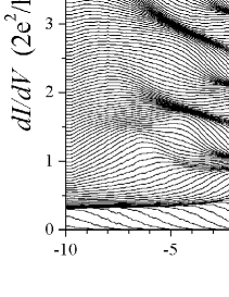
To display the features in the conductance traces more clearly we study the transconductance, , which is calculated by numerical differentiation from the measured differential conductance . The transconductance is zero (or small) on conductance plateaus and shows peaks in the transition regions between plateaus. In Fig. 5 is shown a grayscale plot of the transconductance of sample A, calculated from the data in Fig. 3. The plot covers the range to 10 mV in source-drain bias and 0.25 to 0.50 V in gate voltage corresponding to the first four integer conductance plateaus. Plateau regions (small transconductance) appear as light regions bounded by dark transition regions (high transconductance). The main feature of the plot is the well-known diamond shaped dark transition regions surrounding the integer plateaus and the half-plateaus , where [9, 13]. The transitions in are due to the crossing of the chemical potentials and of the source and drain reservoirs through the subband edges defining the transmitting subbands. The procedure described in Sec. IV A to get rid of the dependence of the plateau values allows for an unambiguous assignment of conductance values in each of the diamonds of the transconductance plot. The subband separation is extracted from the main diamond structure by reading off the value of where the straight black lines surrounding the 1 diamond intersect indicating the appearance of the next subband. The intersection is at . Thus mV as listed in Table I.

C The anomalous subband edge
In addition to the main feature the anomalous conductance plateaus are seen. The most pronounced is the anomalous plateau, which appears in the left-hand side of the diamond between the leftmost black straight edge and a curved gray anomalous transition line. Note how the anomalous transition line is continued smoothly into the diamond. Similar, but much weaker, anomalous structures are seen running inside the 2 diamond continuing into the 2.5 diamond, and inside the 3 diamond continuing into 3.5 diamond.
Just as the black straight lines in the grayscale plot of Fig. 5 are due to the crossing of and through the subband edges of the transmitting subbands, it is tempting to also associate a subband edge crossing with the anomalous transitions. In particular the strong
[ 
]
transition ridge between the 1.0 and the 0.9 plateau can be
analyzed in those terms. In the standard
theory changing for fixed at the first half of the
first plateau leads to the sequence , since
drops below the lowest lying spin-degenerate subband
edge. However, this sequence is not observed in the measurements.
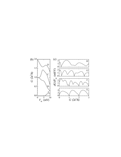
To make this point clear we show in Fig. 6 four
individual traces at fixed , denoted A to D, and four traces at
fixed , denoted E to H. In Fig. 6a these traces
are drawn as dashed lines in the - plane. In
Fig. 6b is shown the differential conductance along trace
A to D.
The zero-bias point of these four traces corresponds to the following
positions on the K conductance curve of
Fig. 2: below the first plateau (A), on the
lower half of the first plateau (B), on the upper half of the first
plateau (C), and on the lower half of the second plateau (D). First
follow trace B. It exhibits the plateau sequence . Probably due to the ’softness’
of the QPC at low electron densities the value of the ’0.5-plateau’ is
around 0.2, where the trace meet with trace A evolving from
into a plateau at . It is as if the conductance in trace B
drops in two steps corresponding to the crossing of two subband edges
rather than just one, perhaps as a consequence of lifting of the
spin-degeneracy in the QPC[7, 15, 17].
It seems quite natural to associate the anomalous transition with an anomalous subband edge which lies above the ordinary subband edge and therefore is encountered first as the bias voltage is raised. This would also account for the continuation of the anomalous transition into the 1.5 diamond as seen by studying the behavior of trace C. Increasing from 0 this trace exhibits a clear plateau at 1.0 before it rises and develops into a plateau at as is raised above the second subband. For slightly larger value of falls below the anomalous subband edge; drops and the trace exhibits a shoulder-like feature around . Only for yet higher values of does drop below the ordinary first subband leading to and lower values as in the standard case. Thus as a function of the bias-voltage the plateau sequences and , for the first and second half of the -plateau, expected from the simple half-plateau model, in experiment are seen rather to be and .
The values of the conductance at the plateaus are found after the fitting procedure described in Fig. 4. The most precise way to obtain these values is through Fig. 6c, where the transconductance is plotted versus the differential conductance at four different but fixed bias voltages, traces E, F, G and H. The plateaus appear as minima in the curves, since a minimum in the the transconductance correspond to the point of least slope in plots of versus . Ideally, if the plateaus are completely flat, the values at the minima are 0. This happens for example at the integer plateaus seen in trace E, and the half-plateaus in trace G. The 0.85-plateau is never completely flat, but in traces F and G it is seen as a well developed minimum.
For comparison with the temperature data presented in Sec.VI we introduce the anomalous gate voltage dependent (and hence density dependent) energy difference . It is related to that particular gate-voltage dependent value of the source-drain bias that maximizes the transconductance along the 0.9-1.0 and 1.35-1.5 ridges in the grayscale plot:
| (9) |
In terms of an anomalous subband, is interpreted as the difference between the chemical potential and the anomalous subband edge. In Fig. 5 it is seen that similar ridges appear, progressively weaker, for the higher subbands. The weakening of the effect may be due to less pronounced spin polarization at the higher densities present when more subbands are occupied [15]. Finally, we note that in contrast to the normal plateaus, the anomalous plateaus only appear when both and are above a given subband edge: the anomalous plateaus only appear in the left-hand side of the diamonds in the grayscale plots. This is another indication that the anomalous plateaus are related to interaction effects and not simple single-particle subband effects.

V The activation temperature
To gain further insight in the conductance anomaly we also study the temperature development of the first conductance plateau, . In Fig. 7 is shown a set of measurements performed on sample A. At the lowest temperature, 0.3 K, the plateau is broad and flat. With a 1D subband energy separation of 6.5 meV, the thermal smearing of the plateau should be negligible at temperatures below 4 K. This is indeed also the case for the upper half of the conductance plateau, mV, which stays flat as the temperature is raised. On the lower half of the plateau, the conductance is suppressed below the plateau value, , as the temperature is raised, developing a plateau-like structure around the conductance value . This is the 0.7 conductance anomaly.
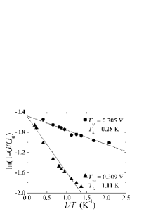
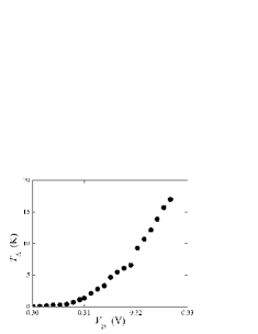
The large 1D-subband energy separation in the shallow etched QPC’s allows us to study the temperature dependence of the -structure at temperatures up to around 5 K without appreciable thermal smearing of the quantized conductance. In Fig. 8 we present two Arrhenius plots of the conductance suppression shown in Fig. 7 at V and 0.309 V. We plot the relative conductance suppression (where is the measured conductance value of the plateau) versus at the given fixed gate-voltage. The linear behavior in the semilogarithmic Arrhenius plot indicate an activated behavior, , with the corresponding activation temperatures, K and 1.11 K, extracted from the two slopes, respectively. Fig. 8b shows how the measured activation temperature as a function of gate voltage increases from 0 at pinch off to a few kelvin at the middle of the conductance plateau.
In the usual framework of the Landauer-Büttiker formalism the observed activated suppression of the conductance indicates that the -structure is associated with thermal depopulation of a subband having a gate voltage dependent subband edge. If a subband edge lies below the Fermi level indeed an activated behavior is seen in . A phenomenological theory along these lines has been presented by Bruus et al. [17]. Moreover, this picture is in accordance with the discussion presented in Sec. IV C of the crossing of subband edges at finite bias. In the following analysis we connect the measured activation temperature with the energy gap found by finite-bias spectroscopy.
VI Comparing and
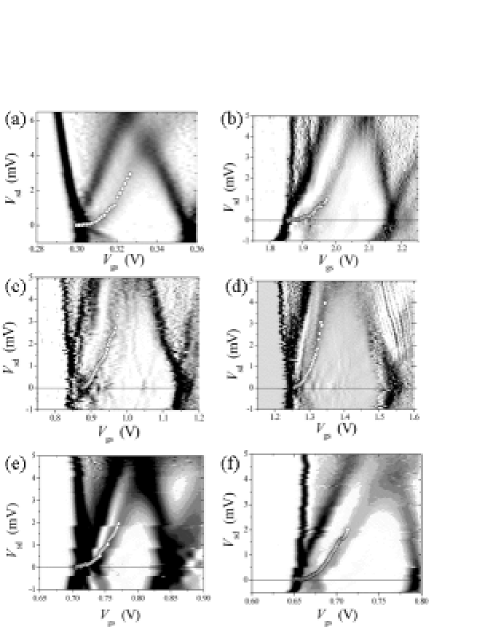
It is possible to ascribe the same origin to the appearance of the plateau at at finite bias as to the 0.7 anomaly. The two effects are connected by the energies and . Consider a fixed gate-voltage on the lower half of the plateau. The data are taken at low temperature. At zero bias the excitation energies available for the electrons at the Fermi energy are not sufficient to reach the subband edge lying below the Fermi level, and the conductance has the expected, quantized value, . As the source-drain bias-voltage, is increased we assume that half the potential drop is before and the other half after the QPC, i.e. in Eq. (3). The electrons from the drain reservoir are injected below the subband edge when . This assumption is supported by our experiments. In Fig. 9 we have for all six samples plotted the expected position of the resonance, , versus gate voltage as white circles. The activation temperature used in this plot is obtained from the measured temperature dependence of the -structure, as the one presented in Figs. 7 and 8. As seen from Fig. 9 the transition from the regular plateau to the anomalous plateau appears at the expected resonance position.
The quality of the 0.7/0.85 anomalies are varying a lot from sample to sample. The exact reason for this is not known at present. One can think of many reasons such as impurities, geometry related defects, and other sample parameters. But it is noteworthy that for all samples the energy characterizing the 0.85 anomaly coincides with the activation energy deduced from the 0.7 anomaly.
VII Conclusion
We have investigated the conductance anomaly in six samples of three different types of shallow etched GaAs/GaAlAS QPC’s: top-gated, side-gated and side-gated, overgrown. We note that the QPC confinement potential depends on both and . The influence from , referred to as self-gating, can explain the distinct asymmetry and non-linearity always observed in differential conductance of QPCs. The QPCs thus appear to be ’soft’, but we have shown how to subtract the self-gating effect from the data. Based on finite bias spectroscopy we have presented experimental evidence, that the 0.7 anomaly is associated with a density-dependent energy difference of the order of a few kelvin being the distance from the chemical potential to an anomalous subband edge. The shallow etching technique gives rise to a strong lateral confinement with 1D subband energy separations of meV. We have therefore been able study the 0.7 anomaly for higher temperatures than for normal split-gate devices, and this allowed a detailed study of the temperature dependence of the conductance anomaly. We have found an activated behavior of the conductance suppression on the anomaly, with a density-dependent activation temperature, , of a few kelvin. For all six samples the energy difference is found to be equal to the activation energy . Our observations supports the idea that the 0.7/0.85 conductance anomaly arises from the existence of an anomalous subband edge in the QPC. The nature of the anomalous subbands is presently unknown. But our observation that the anomalous plateaus only appear when both and are above a given subband edge, and the behavior of the 0.7 anomaly as function of magnetic field [7] indicate the importance of interaction effects beyond the simple single-particle subband picture, presumably related to spin polarization [7, 15, 17].
Acknowledgements
This research is part of the EU IT-LTR programme Q-SWITCH (No. 20960/30960), and was partly supported by the Danish Technical Research Council (grant no. 9701490) and by the Danish Natural Science Research Council (grants no. 9502937, 9600548 and 9601677). The III-V materials used in this investigation were made at the III-V NANOLAB, operated jointly by the Microelectronics Centre of the Danish Technical University and the Niels Bohr Institute fAPG, University of Copenhagen.
REFERENCES
- [1] B.J. van Wees, H. van Houten, C.W.J. Beenakker, J.G. Williamson, L.P. Kouwenhoven, D. van der Marel, and C.T. Foxon, Phys.Rev.Lett. B 60, 848 (1988).
- [2] D.A. Wharam, T.J. Thornton,R. Newbury, M. Pepper, H. Ahmed, J.E.F. Frost, D.G. Hasko, D.C. Peacock, D.A. Ritchie, and G.A. Jones, J.Phys.C 21, L209 (1988).
- [3] H. Van Houten, C.W.J.Beenakker, and B. van Wees, p. 9 in Nanostructured Systems, M. Reed eds., Semiconductors and Semimetals, R.K. Williamson, A.C. Beer and R. Weber eds. (Academic Press, 1992).
- [4] S. Tarucha, T. Honda, and T.Saku, Solid State Commun. 94, 413 (1995)
- [5] A. Yacobi, H.L. Stormer, N.S. Wingreen, L.N. Pfeiffer, K.W. Baldwin, and K.W. West. Phys. Rev. Lett. 77 4612 (1996)
- [6] R.D. Tscheuschner and A.D. Wieck, Superlattices and Microstructures 20 615 (1996)
- [7] K.J. Thomas, J.T. Nicholls, M.Y. Simmons, M. Pepper, D.R. Mace, and D.A. Ritchie, Phys. Rev. Lett. 77, 135 (1996)
- [8] N.K. Patel, J.T. Nicholls, L. Martin-Moreno, M. Pepper, J.E.F. Frost, D.A. Ritchie and G.A.C. Jones Phys. Rev. B 44, 13549 (1991)
- [9] K.J. Thomas, J.T. Nicholls, N.J. Appleyard, M. Pepper, M.Y. Simmons, D.R. Mace, W.R. Tribe and D.A. Ritchie, Phys. Rev. B 58, 4846 (1998)
- [10] C.-T. Liang, M.Y. Simmons, C.G. Smith, G.H. Kim, D.A. Ritchie and M. Pepper, cond-mat/9907379
- [11] A. Kristensen, J.B. Jensen, M. Zaffalon, C.B. Sørensen, S.M. Reimann, P.E. Lindelof, M. Michel, and A. Forchel, J. Appl. Phys. 83, 607 (1998)
- [12] A. Kristensen, P.E.Lindelof, J.B. Jensen, M. Zaffalon, J. Hollinghery, S.W. Pedersen, J. Nygård, H. Bruus, S.M. Reimann, C.B. Sørensen, M. Michel, and A. Forchel, Physica B 249-251, 180 (1998)
- [13] A. Kristensen, H. Bruus, A. Forchel, J.B. Jensen, P.E. Lindelof, M. Michel, J. Nygård, and C.B. Sørensen, cond-mat/9808007
- [14] D. J. Reilly, G. R. Facer, A. S. Dzurak, B. E. Kane, R. G. Clark, P. J. Stiles, J. L. O’Brien, N. E. Lumpkin, L. N. Pfeiffer, K. W. West, cond-mat/0001174
- [15] C.-K. Wang and K.-F. Berggren, Phys. Rev. B 57, 4552 (1998)
- [16] B. Spivak and F. Zhou, cond-mat/9911175.
- [17] H. Bruus, V.V. Cheianov, and K. Flensberg, cond-mat/0002338.
- [18] B.E. Kane, G.R. Facer, A.S. Dzurak, N.E. Lumpkin, R.G. Clark, L.N. Pfeiffer, and K.W. West, Appl. Phys. Lett. 72 3506 (1998)
- [19] L. Martin-Moreno, J.T. Nicholls, N.K. Patel, and M. Pepper, J. Phys.:Condens. Matter 4, 1323 (1992).
- [20] The self-gating resembles the so-called channel length modulation well known from conventional field effect transistors.
- [21] L.I. Glazman and A. V. Khaetskii, Europhys. Lett. 9, 263 (1989).
- [22] N.K. Patel, L. Martin-Moreno, M. Pepper, R. Newbury, J.E.F. Frost, D.A. Ritchie, G.A.C. Jones, J.T.M.B. Janssen, J. Singleton, and J.A.A.J. Perenboom, J. Phys.: Condens. Matter 2 7247 (1990)
- [23] L.P. Kouwenhoven, B.J. van Wees, C.J.P.M. Harmans J.G. Williamson, H. van Houten, C.W.J. Beenakker, C.T. Foxon, and J.J. Harris, Phys. Rev B39, 8040 (1989)