Theoretical interpretation of the experimental electronic structure of lens shaped, self-assembled InAs/GaAs quantum dots
Abstract
We adopt an atomistic pseudopotential description of the electronic structure of self-assembled, lens shaped InAs quantum dots within the “linear combination of bulk bands” method. We present a detailed comparison with experiment, including quantities such as the single particle electron and hole energy level spacings, the excitonic band gap, the electron-electron, hole-hole and electron hole Coulomb energies and the optical polarization anisotropy. We find a generally good agreement, which is improved even further for a dot composition where some Ga has diffused into the dots.
I Introduction: Using theory as a bridge between the structure and the electronic properties of quantum dots
Self-assembled, Stranski-Krastanow (SK) grown semiconductor quantum dots have recently received considerable attention as they exhibit a rich spectrum of phenomena including quantum-confinementhawrylak ; gaponenko ; mrs_feb98 , exchange-splittingslandin98 , Coulomb charging/blockadedrexler94 ; medeiros95 ; fricke96 ; miller97 ; warburton97 ; schmidt97 ; warburton98 ; schmidt98 ; brunkov98 and multi-exciton transitionslandin98 ; dekel98 . Over the past few years a considerable number of high quality measurements of the electronic level stucture of these dot systems have been performed, using photoluminescence (PL)schmidt97 ; schmidt98 ; yang99 ; yang2000 ; berryman97 ; itskevich98 ; itskevich99 ; fry2000 ,photoluminescence luminescence excitation (PLE)landin98 ; dekel98 , capacitancedrexler94 ; medeiros95 ; fricke96 ; brunkov98 and far infra red (FIR) spectroscopyfricke96 ; pan98 ; sauvage99 ; sauvage97 ; pan98:2 . These measurements have been able to determine the electronic level structure to relatively high precision. In parallel with these measurements, several groups have also attempted to measure the geometry and composition of these dotsyang99 ; yang2000 ; metzger99 ; garcia97 ; rubin96 . So far, however, these measurements have failed to provide details of the shape, size, inhomogeneous strain and alloying profiles to a similar level of accuracy to that in which the electronic structure has been determined. As a result, the size of the dots were often used as adjustable parameters in models that fit experimental spectra. For example, using a single-band effective mass model, Dekel et. aldekel98 defined an “effective shape” (cuboid) and “effective dimension” that reproduced the measured excitonic transitions. Similar “parabolic dot” models have been assumed by Hawrylak et. alhawrylak .
The accuracy of single-band and multi-band effective mass methods was recently examined in a series of papers wood96 ; fu_pressure ; wang_cdse ; pryor98:2 ; wang2000 . In these works, the shape, size and composition of nanostructures were arbitrarily fixed, and the electronic structure was evaluated by successively improving the basis set, starting from single-band methods (effective-mass), going to six and eight band methods (k.p), and finally, using a converged, multi-band approach (plane-wave pseudopotentials). It was found that conventional effective-mass and k.p methods can sometimes significantly misrepresent the fully converged results even when the shape, size and composition was given. The observed discrepancies were both quantitative (such as band gap values, level spacings, Coulomb energies) and qualitative (absence of polarization anisotropy in square based pyramidal dotswang2000 , missing energy levelswang_cdse ). As a result of these limitations these methods may not offer a reliable bridge between the electronic structure and atomic structure.
In this paper, we offer a bridge between recent measurements of the electronic structure and measurements of the atomic structure of the dots using accurate theoretical modeling. Modeling can determine if the calculated electronic structure resulting from an assumed shape, size, strain and alloying profiles agrees with the measured electronic structure or not. A theory that can perform such a “bridging function” must be accurate and reliable. The pseudopotential approach to this problem qualifies, in that any discrepancy between the predicted and measured electronic properties can be attributed to incorrectly assumed shape, size or alloying profile. We have studied a range of shapes, sizes and alloy profiles and find that a lens-shaped InAs dot with an inhomogeneous Ga alloying profile is in closest agreement with current measurements. In the following sections we attempt to provide a consistent theoretical interpretation of numerous spectroscopic properties of InAs/GaAs dots.
II Outline of the Method of calculation
We aim to calculate the energy associated with various electronic excitations in InAs/GaAs quantum dots. These energies can be expressed as total energy differences and require four stages of calculation:
(i) Assume the shape, size and composition and compute the equilibrium displacements: We first construct a supercell containing both the quantum dot and surrounding GaAs barrier material. The shape, size and composition profile are taken as input and subsequently refined. Sufficient GaAs barrier is used, so that when periodic boundary conditions are applied to the system, the electronic and strain interactions between dots in neighboring cells is negligible. The atomic positions within the supercell are then relaxed by minimizing the strain energy described by an atomistic force fieldkeating ; pryor98 including bond bending, bond stretching and bond bending-bond stretching interactions (see section III.1). An atomic force field is similar to continuum elasticity approachespryor98 in that both methods are based on the elastic constants, , of the underlying bulk materials. However, atomistic approaches are superior to continuum methods in two ways, (a) they can contain anharmonic effects, and (b) they capture the correct point group symmetry, e.g. the point group symmetry of a square based, zinc blende pyramidal dot is , since the [110] and [10] directions are inequivalent while continuum methodspryor98 , find . More details of the atomistic relaxation are given in section III.1.
(ii) Setup and solve the pseudopotential single-particle equation: A single-particle Schrödinger equation is set up at the relaxed atomic positions,
| (1) |
The potential for the system is written as a sum of strain-dependent, screened atomic pseudopotentials, , that are fit to bulk properties extracted from experiment and first-principles calculations (see section III.2). The Schrödinger equation is solved by expanding in a linear combination of bulk states, , from bands, , and k-points, ,
| (2) |
taken at a few strain values. The solution of Eqs. (1) and (2) provides the level structure and dipole transition matrix elements. More details on the solution of the Schrödinger equation are given in section III.3.
(iii) Calculate the screened, inter-particle many-body interactions: The calculated single particle wavefunctions are used to compute the electron-electron, electron-hole and hole-hole direct , , and exchange Coulomb energies (see section III.4).
(iv) Calculate excitation energies as differences in total, many particle energies: For example, the difference between the total energy of a dot with a hole in level and an electron in level and the total energy of the unexcited dot is
| (3) | |||||
where (in the absence of spin-orbit coupling) for triplet states, and 0 for singlet states. Analagous expressions exist for electron-addition experiments (see section III.4).
The main approximations involved in our method are: (a) the fit of the pseudopotential to the experimental data of bulk materials is never perfect (see Table 1) and (b) we neglect self-consistent iterations in that we assume that the screened pseudopotential drawn from a bulk calculation is appropriate for the dot. Our numerical convergence parameters are (i) the size of the GaAs barrier separating periodic images of the dots, and (ii) the number of bulk wavefunctions used in the LCBB expansion of the wavefunctions. To examine the effects of these approximations and convergences on the ultimate level of accuracy that can be obtained with our methodology we have first applied these methods to an InGaAs/GaAs quantum well(see section III.5), where experimental measurements of the shape, size, composition and transition energies are more established (see section III.5). We next describe the details of our method.
| Property | GaAs | InAs | ||
|---|---|---|---|---|
| EPM | Exptbornstein | EPM | Exptbornstein | |
| 1.527 | 1.52 | 0.424 | 0.42 | |
| -2.697 | -2.96 | -2.330 | -2.40 | |
| 1.981 | 1.98 | 2.205 | 2.34 | |
| 2.52 | 2.50 | 2.719 | 2.54 | |
| -1.01 | -1.30 | -5.76 | -6.30 | |
| 2.36 | 1.81 | 1.668 | 1.71 | |
| 0.066 | 0.067 | 0.024 | 0.023 | |
| 0.342 | 0.40 | 0.385 | 0.35 | |
| 0.866 | 0.57 | 0.994 | 0.85 | |
| 0.093 | 0.082 | 0.030 | 0.026 | |
| -7.88 | -8.33 | -6.79 | -5.7 | |
| -1.11 | -1.0 | -0.826 | -1.0 | |
| -1.559 | -1.7 | -1.62 | -1.7 | |
| 0.34 | 0.34 | 0.36 | 0.38 | |
| 0.177 | 0.22 | 0.26 | 0.27 | |
III Details of the Method of Calculations
III.1 Calculation of equilibrium atomic positions for a given shape
To calculate the relaxed atomic positions within the supercell, we use a generalization (G-VFF) of the original valence force field (VFF)keating model. Our implementation of the VFF includes bond stretching, bond angle bending and bond-length/bond-angle interaction terms in the VFF Hamiltonian. This enables us to accurately reproduce the , and elastic constants in a zincblende bulk material. We have also included higher order bond stretching terms, which lead to the correct dependence of the Young’s modulus with pressure. The G-VFF total energy can be expressed as:
| (4) | |||||
where . Here is the coordinate of atom i and is the ideal (unrelaxed) bond distance between atom types of and . Also, is the ideal (unrelaxed) angle of the bond angle . The denotes summation over the nearest neighbors of atom . The bond stretching, bond angle bending, and bond-length/bond-angle interaction coefficients , , are related to the elastic constants in a pure zincblende structure in the following way,
| (5) |
The second-order bond stretching coefficient is related to the pressure derivative of the Young’s modulus by , where is the Young’s modulus. Note that in the standardkeating VFF which we have used previouslyjkim98 ; williamson99 ; williamson98 the last terms of Eq.(4) are missing, so in Eq.(III.1). Thus there were only two free parameters () and therefore three elastic constants could not, in general, be fit exactly. The G-VFF parameters and the resulting elastic constants are shown in Table 2 for GaAs and InAs crystals. For an InGaAs alloy system, the bond angle and bond-length/bond-angle interaction parameters , for the mixed cation Ga-As-In bond-angle are taken as the algebraic average of the In-As-In and Ga-As-Ga values. The ideal bond angle is 109∘ for the pure zincblende crystal. However, to satisfy Vegas’s law for the alloy volume, we find that it is necessary to use for the cation mixed bond angle.
| GaAs | 32.153 | 9.370 | -4.099 | -105. | 12.11 | 5.48 | 6.04 |
|---|---|---|---|---|---|---|---|
| InAs | 21.674 | 5.760 | -5.753 | -112. | 8.33 | 4.53 | 3.80 |
As a simple test of this G-VFF for alloy systems, we compared the relaxed atomic positions from G-VFF with pseudopotential LDA results for a (100) (GaAs)1/(InAs)1 superlattice where the ratio is fixed to 1, but we allow energy minimizing changes in the overall lattice constant () and the atomic internal degrees of freedom (). We find Å and , while the G-VFF results are Å and . In comparison the original VFF yields Å and .
III.2 The Empirical Pseudopotential Hamiltonian
We set up the single-particle Hamiltonian as
| (6) |
where is the G-VFF relaxed position of the nth atom of type . Here is a screened empirical pseudopotential for atomic type . It contains a local part and a nonlocal, spin-orbit interaction part.
The local potential part is designed to include dependence on the local hydrostatic strain Tr:
| (7) |
where the is a fitting parameter. The zero strain potential is expressed in reciprocal space q as
| (8) |
The local hydrostatic strain for a given atom at is defined as , where is the volume of the tetrahedron formed by the four atoms bonded to the atom at . is the volume of that tetrahedron in the unstrained condition. The need for explicit dependence of the atomic pseudopotential on strain in Eq.(7) results from the following: While the description in Eq.(6) of the total pseudopotential as a superposition of atomic potentials situated at specific sites, , does capture the correct local symmetries in the system, the absence of a self-consistent treatment of the Schrödinger equation deprives the potential from changing in response to strain. In the absence of a strain-dependent term, the volume dependence of the energy of the bulk valence band maximum is incorrect. While self-consistent descriptions show that the volume deformation potential of the valence band maximum is negative for GaAs, GaSb, InAs, InSb and for all II-VI this qualitative behavior can not be obtained by a non-self-consistent calculation that lacks a strain dependent pseudopotential.
The nonlocal part of the potential describes the spin-orbit interaction,
where is a projector of angular momentum centered at , is the spatial angular momentum operator, is the Dirac spin operator, and is a potential describing the spin-orbit interaction.
In Eq(6), the kinetic energy of the electrons has been scaled by a factor of . The origin of this term is as follows: In an accurate description of the crystal band structure, such as the GW methodhedin99 , a general, spatially non-local potential, , is needed to describe the self-energy term. In the absence of such a term the occupied band width of an inhomogeneous electron gas is too large compared to the exact many-body result. To a first approximation, however, the leading effects of this non-local potential, , can be represented by scaling the kinetic energy. This can be seen by Fourier transforming in reciprocal space, , then making a Taylor expansion of about zero. We find that the introduction of such a kinetic energy scaling, permits a simultaneous fit of both the effective masses and energy gaps. In this study, we fit for both GaAs and InAs.
The pseudopotential parameters in Eqs(7) and (8) were fitted to the bulk band structures, experimental deformation potentials and effective masses and first-principles calculations of the valence band offsets of of GaAs and InAs. The alloy bowing parameter for the GaInAs band gap (0.6 eV) is also fitted. The pseudopotential parameters are given in Table 3 and their fitted properties are given in Table 1bornstein . We see that unlike the LDA, here we accurately reproduce the bulk band gaps and the bulk effective masses. One significant difference in our parameter set, to that used in conventional k.p studies, is our choice of a negative magnitude for the valence band deformation potential, , which we have obtained from LAPW calculationsfranceschetti94 .
| Parameter | In | Ga | As (InAs) | As (GaAs) |
|---|---|---|---|---|
| a0 | 644.13 | 432960 | 26.468 | 10.933 |
| a1 | 1.5126 | 1.7842 | 3.0313 | 3.0905 |
| a2 | 15.201 | 18880 | 1.2464 | 1.1040 |
| a3 | 0.35374 | 0.20810 | 0.42129 | 0.23304 |
| a4 | 2.1821 | 2.5639 | 0.0 | 0.0 |
The present InAs and GaAs pseudopotentials have been systematically improved relative to our previous InAs and GaAs potentialsjkim98 ; williamson99 ; williamson98:2 ; wang99 ; wang99:2 , although the functional form has remained the same. Firstly, the pseudopotentials for InAs and GaAs used in Ref.jkim98 ; wang99 did not include the spin-orbit interaction. In Refs.williamson98:2 ; williamson99 ; wang99:2 we used potentials that included the spin-orbit interaction, but were not able to simultaneously, accurately fit the electron effective and the zone center band gap, due to the lack of the above parameter. The potential used here is identical to that used in Refs.wang99 ; wang2000 .
III.3 Calculating the single particle eigenstates
One could use a straight forward expansion of the single particle wavefunctions in a plane wave basis set, as we have previously done in Refs.williamson98 ; williamson99 ; jkim98 . However, as was shown in Refs.wang99 ; wang2000 ; wang97:2 , a more economical representation is to use the Linear Combination of Bulk Bands (LCBB) methodwang99 ; wang2000 ; wang97:2 . Within the LCBB the eigenstates of the pseudopotential Hamiltonian are expanded in a basis of bulk Bloch orbitals
| (10) |
where is the cell periodic part of the bulk Bloch wavefunction for structure, , at the band and the kth k-point, . These states form a physically more intuitive basis than traditional plane waves therefore the number of bands and k-points can be significantly reduced to keep only the physically important bands and k-points (around the point in this case). This method was recently generalized to strained semiconductor heterostructure systemswang99 and to include to spin-orbit interactionwang99:2 . In this paper use an LCBB basis derived from four structures, . These structures are (i) unstrained, bulk InAs at zero pressure, (ii) unstrained, bulk GaAs at zero pressure, (iii) bulk InAs subjected to the strain value in the center of the InAs dot, and (iv) bulk InAs subjected to the strain value at the tip of the InAs dot. By interpolating the strain profile between these four structures, the basis is able to accurately describe all the strain in the system. The wavevectors, , used here include all allowed values within of the zone center, where is the supercell size. For calculations of electron states, the band indices, , include only the band around the point. For the hole states we also include the three bands around the point. This basis set produces single particle energies that are converged with respect to basis size, to within 1 meV.
III.4 Constructing the energies of different electronic configurations
Using screened Hartree Fock theory, the energy associated with loading electrons into a quantum dot can be expressedfranceschetti2000 as
| (11) |
where are the single-particle energies and are the polarization self-energies of the electron state , and are the direct and exchange Coulomb integrals between the and electronic states and are the occupation numbers (). As shown in Ref.franceschetti2000 , for free standing, colloidal quantum dots the dielectric constant inside the dot is dramatically different to that outside (vacuum) and hence the polarization self-energy, , is very significant (1 eV). For self assembled InAs dots embedded in GaAs, the dielectric constants of InAs and GaAs are similar () and we calculate this term as 1 meV, and hence we choose to neglect it here. The direct and exchange Coulomb energies, are defined as
| (12) |
where is a phenomenological, screened dielectric functionwilliamson98:2 containing a Thomas Fermi electronic component and an ionic component from Ref.haken . Our exchange automatically includes both short and long range components.
Denoting electron levels as …, hole levels as … and the number of electrons and holes as and , the total energy, , is
| (13) | |||||
where and are the electron and hole occupation numbers respectively and and . Using Eq.(13), in the strong confinement regime where kinetic energy effects dominate over the effects of exchange and correlation, an exciton involving electrons excited from hole state to electron state can be expressed as
| (14) |
To study charged dots, if one assumes the electron states are occupied in order of increasing energy (Aufbau principle), the total energy of a dot charged with electrons, , is
| (15) | |||||
As indicated in section II, our wavefunctions, , are not iterated to self-consistency. This affects the magnitude of the direct and exchange Coulomb integrals. We have previously examined the accuracy of this perturbative treatment for colloidal InAs dots by comparing the non-self-consistent Coulomb energy with that obtained self consistentlyfranceschetti97 . The differences were negligible.
III.5 Quantum well tests
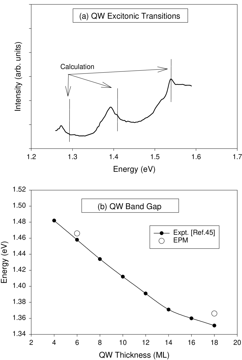
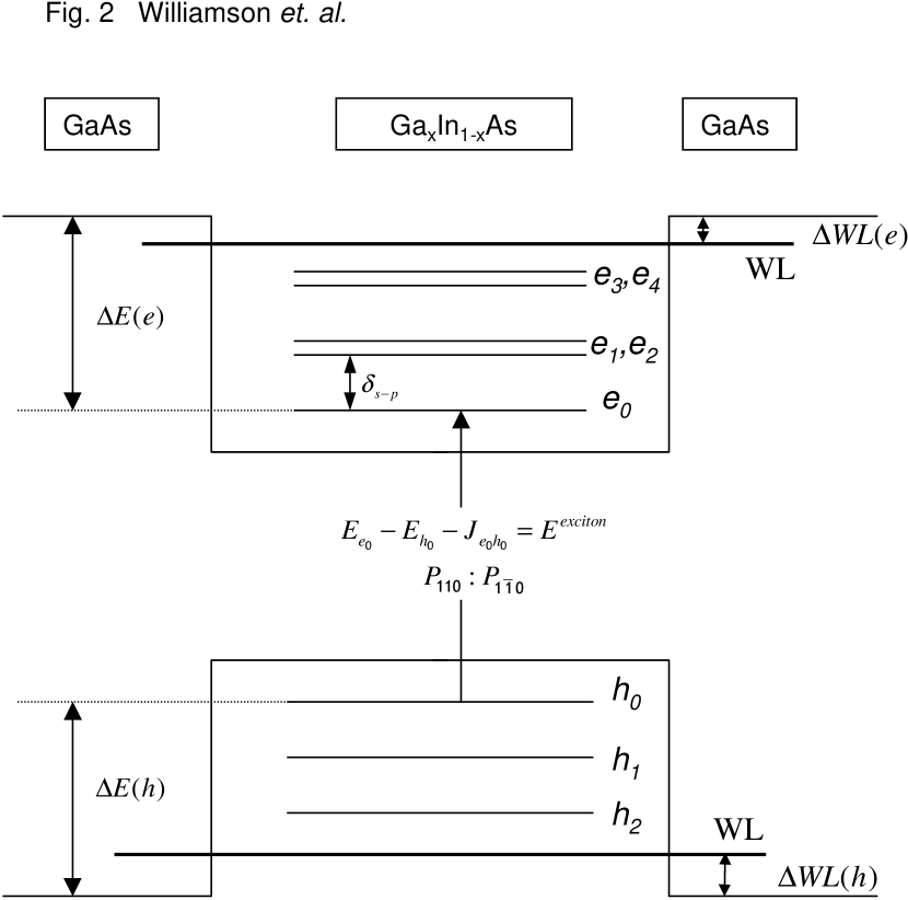
To test the above methods, we first calculated the energy levels in a quantum well, and compared the results with experiment. In Fig. 1(a), we compare the calculated electron-heavy hole transition energies for a 96 Å In0.24Ga0.76As quantum well inside a GaAs matrix. The peaks in the experimental spectra occurgershoni89 at 1.275, 1.395 and 1.538 eV. Our calculated transitions occur at 1.290, 1.404 and 1.545 eV respectively. Figure 1(b) compares the band gap of a In0.22Ga0.78As quantum well as a function of its thickness. The measured band gapslaymarie95 for quantum wells with thicknesses of 6 and 18 ML are 1.458 and 1.351 eV. Our calculated values are 1.466 and 1.366 eV.
IV Physical quantities to compare with experiment
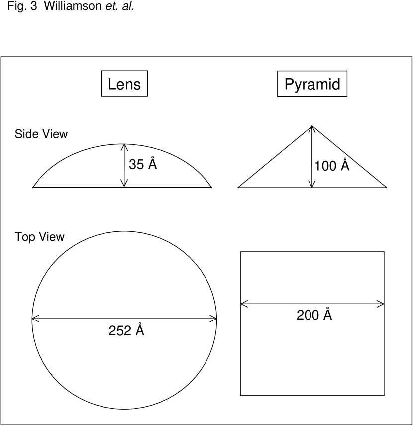
The quantities we use to characterize the electronic structure are illustrated in Fig. 2 which shows a schematic layout of the electron and hole single-particle energy levels in a quantum dot. Assuming that all levels are spatially nondegenerate (thus having only spin degeneracy), we mark the electron levels as …. and the hole levels as . The level is sometimes called “s-like”, whereas and are called “p-like”, and and are called “d-like”. Since the GaAs environment of the InAs dots is largely unstrained, it is convenient to set as a reference energy the VBM of GaAs as , and the CBM of GaAs as E=1520 meV. All energy levels can be referenced with respect to these band edges.
For the electron levels, the quantities that we consider are:
(i) The number of dot-confined electron states, .
(ii) The spacing between “s-like” and “p-like” electron states.
(iii) The splitting between the “p-like” electron states.
(iv) The spacing between “p-like” and “d-like” electron states.
(v) The “binding energy” of the first electron level, , with respect to the GaAs conduction band minimum, .
(vi) The position of the bottom of the band for the 2D InAs “wetting layer” (WL) with respect to the GaAs CBM, .
(vii) Inter-electron direct and exchange Coulomb energies.
For the hole levels we consider are:
(i) The number, , of dot-confined hole states.
(ii) The intra-band spacings of the hole levels, .
(iii) The “binding energy” of the first hole level, , with respect to the GaAs valence band maximum, .
(iv) The position of the top of the band for the 2D InAs “wetting layer” (WL) with respect to the GaAs VBM, .
(v) Inter-hole direct and exchange Coulomb energies.
Finally, for the recombination of electrons and holes, we consider:
(i) The excitonic energies, , as defined in Eq.(14). By subtracting calculated values for the single particle energies and from measured optical excitation energies one can estimate the electron-hole direct Coulomb energies .
(ii) The ratio of absorption intensities for light polarized along [110] and [10] directions, defined as
| (16) |
This ratio can deviate from unity due to three reasons; (a) The dots has different dimensions in the [110] and [10] directions. We refer to this as the the “geometric factor”. (b) The atomistic zincblende symmetry makes the two directions symmetry inequivalent even if the lengths along the two directions are equal. We refer to this as the “atomic symmetry factor”. One manifestation of this affect is that if the strain is calculated atomistically, it is different in the two directions even in the absence of a geometric factorpryor98 . (c) A piezoelectric field that breaks the symmetry. Previous studiesyang2000 have shown that this effect is negligible in InAs/GaAs dots so we will neglect it here. k.p calculations neglect the “atomic symmetry” factor (except for the small effect of strain asymmetry), but retain the “geometric factor”. Pseudopotential calculations retain both effects. For example, in a square based pyramid (where by definition the “geometric factor” does not contribute), k.p produces , while pseudopotential theory gives (see Table 5). This shows that there is not a simple mapping from dot shape to polarization anisotropy, .
(iii) Excitonic dipole: As the center of the electron and hole wavefunctions do not exactly coincide with each other, it is possible that an exciton will exhibit a detectable dipole moment,
| (17) |
V Theoretical Results
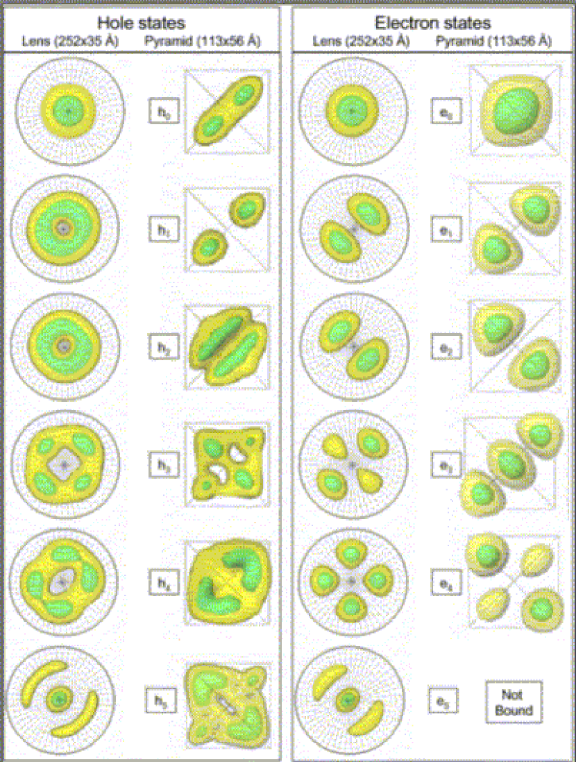
The electronic structure of a series of GaInAs/GaAs self-assembled quantum dots was calculated using the methodology described in Section II. We have chosen to focus on the well established “lens shaped” dot geometry from Refs.drexler94 ; medeiros95 ; fricke96 ; miller97 ; warburton97 ; schmidt97 ; warburton98 ; schmidt98 . The shape of this dot is shown in Fig. 3. The profile is obtained by selecting the section of a pure InAs sphere that yields a circular base with diameter 252Å and a height of 35 Å. The main experimental uncertainty about this dot is the composition profile. It is not known if the dots are pure InAs or if Ga has diffused into the dots. For comparison, we also calculate the electronic structure of a square based InAs pyramid with a base of 113Å and a height of 56Å. This is not believed to be a realistic geometry, however, it has been used as a benchmark for many previous theoretical calculationswang2000 ; jkim98 ; williamson99 ; grundman95 ; jaros96 and we include it here for comparison purposes. In the following sections these two geometries will be referred to as the “lens” and the “pyramid”. The results of our calculations are shown in Table 5 and Fig. 4.
V.1 Confined electron states
Figure 4 shows the calculated square of the envelope function for the electron states in the pyramidal and lens shaped InAs/GaAs quantum dots. For the lens shaped dot, the electron states can be approximately interpreted as eigenstates of the operatorhawrylak . Here we plot only the first 6 bound states corresponding to and . The first state , has and is commonly described as -like as it has no nodes. The and states have , and are -like with nodal planes (110) and (10). The and states have and 0 respectively and are commonly described as , and respectively. Due to the underlying zincblende atomistic structure, the symmetry is reduced to . Hence, the to states correspond to the and irreducible representations of the group, rather than eigenstates of . This allows states and to couple. This coupling is evident, for example, in the larger charge density along [110] compared to [10] in the state, due to its coupling with . The observable effect of this symmetry is to split the and -states, , and the and -states, . The alignment of the and -states states along the [110] and [10] directions also results from the underlying zincblende lattice structure. Note, this analysis neglects the effects of the spin-orbit interaction which reduces the group to a double group with the same single representation for all the states. In our calculations the spin-orbit interaction is included, but is produces no significant effects for the electron states.
The electron states in the pyramidal dot also belong to the group and show a one-to-one correspondence with those in the lens shaped dot. However, there are only 5 bound states in the pyramidal dot due to its smaller size. Here we define an electron state as bound if its energy is below that of the unstrained, bulk GaAs conduction band edge.
The calculated values of the - and - energy spacings, , and, , for the lens and pyramidal shaped dots are 65 and 68 meV and 108 and 64 meV respectively. The splitting of the two states, are 2 and 26 meV respectively. The calculated values of the electron binding energy, , are 271 and 171 meV respectively. The electron-electron direct Coulomb energies, , and in the lens and pyramidal dots are calculated as 32, 25 and 25 meV and 40, 35 and 36 respectively. On applying a magnetic field in the growth direction, we calculate an increase in the splitting of the two states () in the lens shaped dot from 2 to 20 meV. Details of this magnetic field calculation will be given in a future publicationshumway2000 . Finally, the energy of the electron wetting layer level, , with thicknesses of 1 and 2 ML is 15 and 24 meV below the CBM of unstrained bulk GaAs.
V.2 Confined hole states
Figure 4 shows calculated wavefunctions squared for the hole states in pyramidal and lens shaped InAs/GaAs quantum dots. Unlike the electron states, the hole states cannot be approximated by the solutions of a single band Hamiltonian. Instead there is a strong mixing between the original bulk Bloch states with and symmetry. The larger effective mass for holes results in a reduced quantum confinement of the hole states and consequently many more bound hole states. Only the 6 bound hole states with the highest energy are shown in Figure 4.
The calculated values of the - , - and - hole level spacings for the pyramidal and lens shaped dots are 8,7 and 6 meV and 15, 20 and 1 meV respectively. The calculated hole binding energies, , are 194 and 198 meV. We calculate the highest energy hole level in pure InAs wetting layers, , with thicknesses of 1 and 2 ML to reside 30 and 50 meV above the VBM of unstrained bulk GaAs. The hole-hole Coulomb energies, , are 25 and 31 meV.
V.3 Electron-hole excitonic recombination
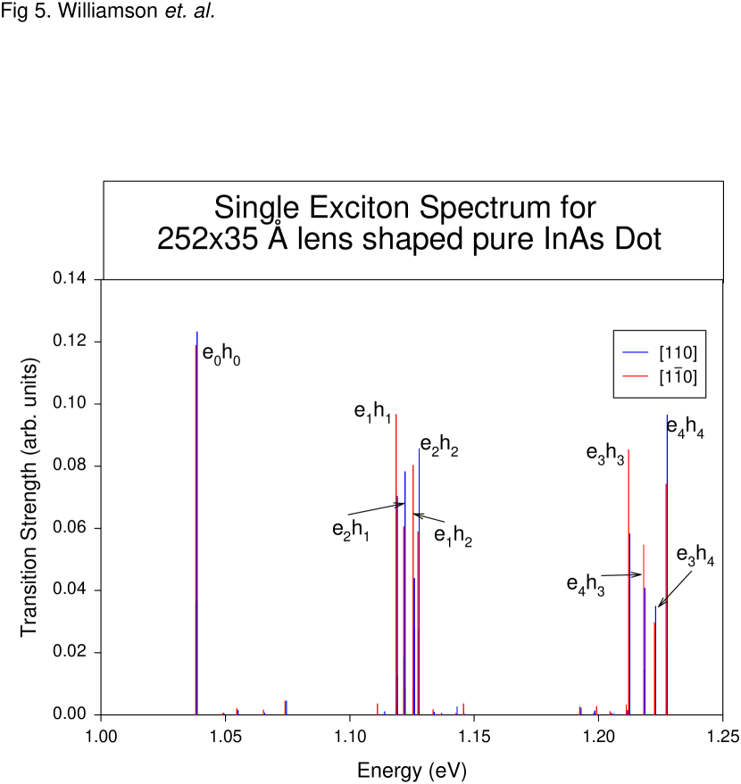
Figure 5 shows our calculated single exciton absorption spectrum for a pure InAs, lens shaped dot with a base of 252 Å and a height of 35 Å. The energies of each of the absorption peaks are calculated from Eq.(14). The ratios of the dipole matrix elements for light polarized along [110] and [10] are calculated from Eq.(16). Figure 5, illustrates that, for a lens shaped dot, both the conventional transitions and additional, and transitions are strongly allowed. The ratio of the polarization anisotropies, , are shown in Table 4. As a result of the circular symmetry of the lens shaped dot, we calculate a polarization ratio of for the transition. This value is in contrast to that calculated value for a pyramidal dot of wang99:2 . For the higher angular momentum transitions we find larger deviations from unity. The magnitude of the ratios, follows the polarization of the wavefunctions shown in Fig. 4. For example we find ratios greater and then less than unity for the and transitions, as reflected by the elongations of the and wavefunctions along the [110] and [10] directions.
| Lens | Pyramid | |
|---|---|---|
| Geometry | 252x35Å | 200x100Å |
| % Ga at base,tip,average | 0,0,0 | 0,0,0 |
| 1.03 | 1.20 | |
| 0.82 | 2.40 | |
| 1.27 | 0.52 | |
| 0.73 | 4.26 | |
| 1.23 | 0.63 |
We calculate ground state electron-hole direct Coulomb energies, , of 37 and 31 meV in the lens shaped and pyramidal dots. The calculated ground state electron-hole exchange energies, are an order of magnitude smaller, with values of 3 and 0.2 meV. These yield excitonic band gaps of 1.03 and 1.12 respectively. The calculated polarization anisotropy ratios [Eq.(16)] for light polarized along [110] and [10] directions are and 1.20 for the lens and pyramidal shapes respectively. The calculated excitonic dipoles [Eq.(17)] are -3.1 and 0.16Å respectively. A positive dipole is defined as the center of the hole wavefunction being located above the center of the electron wavefunction.
VI Analysis of pertinent experimental measurements
VI.1 The intra-band - and - electron energy spacings
Measurements of the spacing between the and like electron levels (-like and -like) are based on infra red absorption. For the lens shaped dots, Fricke et. al.fricke96 load electrons into the dots by growing a sample consisting of a n-type doped layer, a tunneling barrier, a layer of InAs/GaAs lens shaped dots, a GaAs spacer and a GaAs/AlAs short period superlattice (SPS). By applying a voltage between the n-doped layer at the bottom of the sample and a Cr contact grown on top of the SPS, electrons are attracted from the n-doped layer into the InAs dots. Infra-red photons were used to excite electrons from the occupied level into the level. Neglecting the small exchange energy, the energy differences for the excitations when 1 and 2 electrons are present in the dot are
| (18) |
The first of these energy differences yields a direct measurement of the energy spacing, , of 49.1 meV. The second energy difference was measured at 50.1 meV. Drexler et. al.drexler94 also used infra red transmission spectroscopy to measure the energy spacing, meV. Pan et. al.pan98 ; pan98:2 have also performed infra-red absorption measurements on truncated pyramidal dots with a base of 180 Å and height of 60 Å. In these experiments, no gate voltage is applied, and therefore the excitations take place from the ground state of the samples, . They observe multiple infra-red absorption peaks between 89 and 103 meV. These could be associated either with the - spacing of the electron levels or spacings of the hole states (see below).
Itskevich et. al.itskevich99 perform high power PL measurements of pyramidal dots with a base of 150 Å and a height of 30 Å . This high power excitation is able to simultaneously load multiple excitons into the dots. Due to state filling, these multiple excitons will occupy ground state () and higher () single particle levels. Therefore the PL measurements are able to simultaneously measure recombination between electrons occupying the and levels with holes in the and levels. In general, to describe the total energy differences associated with decay from to excitons occupying a dot requires a treatment that includes the exchange and correlation between multiple occupational configurations of the and excitonic states. Such a configurational interaction (CI) approach has previously been considered for model parabolic dotshawrylak and will be discussed for realistic dots in a future publicationwilliamson2000:2 . For the purposes of this discussion, we limit ourselves to discussing the energy differences associated with the lowest energy configurations on the exciton state, i.e. those predicted by the Aufbau principle. Within this approximation, the peaks in the high power, PL spectra can be interpreted as corresponding to [see Eq.(III.4) where exchange is neglected]
| Peak 1: | |||||
| Peak 2: | |||||
| Peak 3: | (19) | ||||
Note, peak 3 is not assigned to a recombination from to as this is almost degenerate with peak 2. Itskevich et. al. assume that (i) the Coulomb integrals in the square brackets on the right hand side of Eq.(VI.1) cancel, (ii) that , and (iii) that the hole spacings, , are small compared to the electron level spacings. With these assumptions the spacings between peaks 1 and 2 and peaks 2 and 3 can be assigned to the - and - energy spacings. They find spacings and of 75 and 80 meV respectively. Our calculations suggest that assumptions (i), (ii) and (iii) probably introduce errors of 10, 5 and +10 meV respectively. The neglect of exchange interactions in the above discussion also introduces an error of 5 meV.
VI.2 The intra-band electron level splitting
For the lens shaped dots, the Capacitance Voltage spectroscopy of Fricke et. al.fricke96 can be used to estimate the splitting of the states, , by loading two electrons into the dot and exciting them using FIR spectroscopy. The relevant energy differences are
| (20) |
By assuming , the difference in the two above expressions yields the energy spacing . They find a value of 2 meV. To measure the effect of a magnetic field on the splitting of the states Fricke et. al.fricke96 use infra-red absorption to measure the above energy differences in an applied magnetic field. At a field of 15 Tesla they measure an energy spacing of 19 meV. More theoretically, Dekel et. aldekel98 have demonstrated that one must assume a splitting of the states to explain the number of multi-exciton levels observed in their single dot, micro PL measurements.
VI.3 The intra-band hole energy spacings
There are currently no measurements available for the energy spacings between the hole states in the lens shaped dots. Itskevich et. al.itskevich99 have performed high power PL measurements of dots estimated to be square based, truncated pyramids with a base of 150Å and a height of 30Å , under hydrostatic pressure to estimate hole level spacings. At hydrostatic pressures above 55 kbar, they measure the PL associated with transitions from the -state in the GaAs matrix to the and levels in the dots. They estimate a hole level spacing of 15 meV. However, the nature of the initial and final hole states is unclear.
Sauvage et. al.sauvage99 use polarized photoinduced intraband absorption spectroscopy to measure the energy spacing between the lowest hole state, , and the hole state with a single node in the growth direction, . This corresponds to [see Eq.(III.4)]
| (21) | |||||
By assuming that Sauvage et. al. estimate the spacing to be 120 meV. Note is almost certainly higher in energy than states with nodes perpendicular to the growth direction ( and ) due to the smaller dimension of the dot in the growth direction. Consequently, the energy difference is not the spacing of the first two hole states -.
Tang et. al.tang98 measure activation energies for excitations from and to the hole wetting layer of 48 and 30 meV respectively, implying an - spacing of 18 meV.
VI.4 The electron and hole binding energies, and
There have been no direct measurements of the electron or hole binding energy for lens shaped InAs dots. However, it has been measured in other dots by several groups using a range of techniques. Berryman et. al.berryman97 placed pyramidal InAs dots estimated to have a base of 100 Å and height of 15 Å in a p-n junction and measured the temperature dependence of the ac conductance as a function of frequency. These measurements predict a hole binding, , energy of 240 meV. When subtracted from the bulk GaAs band gap, this yields a value for the electron binding energy, , of 60 meV. The authors obtain similar results from temperature dependent Hall measurements of thermal hole trapping. Itskevich et. al.itskevich98 measured the pressure at which PL measurements could detect a -X crossing in pyramidal InAs/GaAs quantum dot samples. By extracting these PL measurements back to zero pressure they were able to extrapolate a value for the electron binding energy, , of 50 meV. Itskevich et. al.itskevich99 also used high pressure PL to measure the energy difference between the level in bulk GaAs and the level in the quantum dots. By extrapolating this value back to zero pressure, they predict a value for the hole binding energy, , of 250 meV. Brunkov et. al.brunkov98 performed capacitance-voltage spectroscopy measurements, which when fitted to a capacitance model for their dot geometry predict an electron binding energy of 80 meV for dots with bases of 250 Å. Tang et. al.tang98 measured the spacing of the electron wetting layer to both the GaAs CBM and the level and hence deduced a value for the electron binding energy, , of 80 meV, for dots with an estimated base of 130 to 170 Å.
VI.5 The position of the electron and hole wetting layer level
The presence of a distinct wetting layer signal in the PL spectra of a sample of self assembled quantum dots is the hallmark of a high quality sample. In samples where the wetting layer has “dissolved” due to the growth conditions, it is likely that the geometry and composition of the quantum dots will also have dramatically altered from their uncapped state.
In the lens shaped InAs dots Schmidt et. al.schmidt97 observe PL emission from the ground state of the wetting layer at 1.34 eV. Photovoltage measurementsschmidt97 on the same samples show a strong peak corresponding to absorption into the ground state of the wetting layer at 1.35 eV. There are currently no measurements available for the position of the individual electron and hole wetting layers in the lens shaped InAs/GaAs quantum dot samples. In Ref.sauvage97 Sauvage et. al. grow lens shaped InAs dots with an estimated base of 150 Å and a height of 30 Å on a substrate that is n-doped with silicon. This n-doping loads electrons into the state in the dot, which they excite into the wetting layer using infra-red excitation. In these samples they estimate the wetting layer to be 150 meV above the level. In Ref. sauvage99 Sauvage et. al. load electrons into the state of similar dots using an optical interband pump. Subsequent infra-red absorption places the wetting layer 190 meV above the state. Tang et. al.tang98 measure thermal transfer of holes to the wetting layer, and obtain a spacing between the level and the hole wetting layer, of 48 meV. They also measure thermal transfer from an excited state, possibly involving , which places the hole wetting layer 30 meV below the level.
VI.6 The number of confined electron and hole states
The actual number of confined electron and hole states in a self assembled InAs/GaAs quantum dot depends on the size and composition of the dot. Early single band, effective mass calculationsgrundman95 for pure InAs pyramidal dots with a base of 120 Å and height 60 Å predicted only a single bound electron state and several bound hole states. Consequently, many experiments were then interpreted in this light. More accurate multi-band stier99 ; jiang97 ; jaros96 and pseudopotentialjkim98 ; williamson99 calculations have predicted 5 or more bound electron states in the same dots.
The high power PL experiments of Itskevich et. al.itskevich99 show the gradual disappearance of 5 peaks as a function of external pressure. This is interpreted as direct evidence for 5 confined electron levels in their samples. The single dot, multi-exciton measurements of Dekel et. al.dekel98 require the assumption of at least 3 bound electron states to explain their experimental spectra. Similarly, the capacitance-voltage spectroscopy of Fricke et. al.fricke96 shows two peaks corresponding to the capacitance of -like states and the nearly degenerate -like states, providing evidence for at least 3 bound electron states.
VI.7 Electron and hole Coulomb and Exchange Interactions
By loading multiple electrons and holes into quantum dots it is possible to measure the Coulomb and exchange interactions between these additional electrons and holes. The magnitude of these interactions is a function of the shape of the electronic wavefunctions (see section II) and provides an additional quantity to test the accuracy of theoretical models.
To study electron-electron interactions, Fricke et. al.fricke96 use the same experimental setup discussed in section VI.1. From Eq.(III.4) we see the energy differences corresponding to the peaks in the Capacitance Voltage (CV) spectra associated with loading one and two electrons into the level in the dots is
| (22) |
The electron-electron Coulomb interaction, , can therefore be directly measured as the splitting of these two CV peaks. They find a value of 23 meV. From Eq.(VI.1) we see that
| (23) |
Finally by fitting 4 equidistant bell curves to the CV spectra corresponding to loading 3,4,5 and 6 electrons into the dots, an approximate value for the charging energy between the states, , of 18 meV is obtained. From Eq.(III.4) we that the spacing , while and hence the approximation of equidistant peaks will introduce some error into this estimate for .
VI.8 Electron-hole excitonic recombination
To our knowledge there have so far been no measurements of the polarization anisotropy in the lens shaped dots discussed here. The polarization anisotropy for excitonic recombination in InAs/GaAs was measured by Yang et. al.yang99 ; yang2000 , who find a ratio of and for InAs dots whose geometry is measured to be formed by four {136} faceted planes with bases ranging from 150 to 250 Å and a base to height ratio of 4:1. Yang et. al.yang99 ; yang2000 have performed k.p calculations for this dot geometry, which include the “geometric factor” but not the “atomic symmetry factor” discussed in section IV. They find and . The authors suggest the k.p simulations of the measured polarization ratio can be used to deduce the geometric shape anisotropy. However, we demonstrate here that when the “atomic symmetry factor” is included an anisotropy of is obtained even for a square based pyramid. Thus k.p simulations lacking the “atomic symmetry” factor can not be used to reliably deduce the geometric shape anisotropy.
To our knowledge there have so far been no measurements of the excitonic dipole in lens shaped InAs dots. Fry et. al.fry2000 used photocurrent spectroscopy within an applied electric field to measure the excitonic dipole moment, , [Eq.(17)]. They find the center of the hole wavefunctions to be located 4 Å above the center of the electron wavefunction (positive dipole). Fry et. al.fry2000 also perform single-band, effective mass calculations, in an attempt to isolate the origin of this dipole. They predict that in the absence of alloying the dipole is -3 Å, i.e. the opposite sign , but a linear composition profile with Ga0.5In0.5As at the base and pure InAs at the top of a truncated pyramid with a base of 155 Å, and height 55 Å, reproduces the correct dipole of 4 Å. They suggest that this alloying profile explains the observed dipole. We have repeated these calculations and confirm that, within a single-band model, such a composition profile causes both electrons and holes to move up in the dot compared to their positions in a pure InAs dot. The heavier effective mass of the holes, results in less kinetic energy associated with confinement at the top of the dot and hence the holes move up more than electrons on the introduction of Ga, producing the correct dipole. However, when we repeat these calculations in the more sophisticated, multi-band LCBB basis used here, we find significant heavy hole-light hole mixing in the state, which acts to reduce the above effect and produce a smaller dipole of 1 Å, in contradiction with experiment (+4 Å). We therefore conclude that in a more complete calculation the shape and alloy profile postulated by Fry et. al.fry2000 does not produce the observed excitonic dipole.
VII Comparison of experiment and theory
In Table 5 we show the results of our calculations for pure InAs, lens shaped quantum dots embedded within GaAs [column (a)]. Table 5 also shows the experimentally measured splittings of the electron levels, the electron-electron and electron-hole Coulomb energies, the magnetic field dependence and the excitonic band gap measured in Refs.fricke96 and warburton98 . The agreement between the measured energy level spacings, Coulomb energies and magnetic field response with our theoretical lens shaped model is generally good. Both the model and experiment find (i) a large spacing, , (50-60 meV) between the -like state and the -like state, (ii) a small spacing, , (3 meV) between the two -like and states and (iii) a large spacing (55 meV) between the -like state and the -like state.
These electron level spacings are similar to those found for pyramidal quantum dotsjkim98 (see Table 5). However, in the pyramidal dot, the spacings of the two -like and -like states, , is larger (26 and 23 meV) as a result of the lower C2v symmetry of a zincblende pyramid. Both the model and experiment also find similar values for the Coulomb energies, and (25 meV).
The calculated hole binding energy of meV is in good agreement with those of Berryman et. al.berryman97 (240 meV) and Itskevich et. al.itskevich99 (250 meV). Our calculated electron binding energies, , are considerable larger (271 meV) than those of Berryman et. al.berryman97 (60 meV) and Tang et. al.tang98 (80 meV). We attribute this difference to the larger size of our dots. The assumption of a pure InAs dot also affects the comparison. The agreement improves when we include Ga in our dots (see section VII.2).
The calculated electron-electron and electron-hole Coulomb energies are in reasonable agreement with those extracted from Refs.fricke96 and warburton98 . For the integrals and we calculate values of 31, 25, 25 and 37 respectively, compared to measured values of 23, 24, 18 and 33.3 meV
The calculated polarization anisotropies, , for the recombination in lens and pyramidal shaped, pure InAs dots are and 1.2 respectively. A future measurement of this anisotropy ratio for lens shaped dots would provide an important piece of evidence for determining the detailed geometry of the dots.
In the lens shaped dot we find a difference in the average positions of the and states, , of around 1 Å. This is smaller than the value we calculate for a pyramidal quantum dot, where we find the hole approximately 3.1 Å higher than the electron.
In summary, the assumed lens shaped geometry, with a pure InAs composition produces a good agreement with measured level splitting, Coulomb energies and magnetic field dependence. A closer inspection of the remaining differences reveals that the calculations systematically overestimate the splittings between the single particle electron levels (: 65 vs. 50 meV, :68 vs. 48 meV) and underestimates the excitonic band gap (1032 vs. 1098 meV).
VII.1 Pure InAs dots: The effects of shape and size
Focusing on the lens shape only, we examine the effect of changing the height and base of the assumed geometry. Calculations were performed on similar lens shaped, pure InAs dots where (i) the base of the dot was increased from 252 to 275Å, while keeping the height fixed at 35Å, [column (b)] and (ii) the height of the dot was decreased from 35 to 25Å, while keeping the base fixed at 252Å, [column (c)]. It shows that decreasing the height of the dot increases the quantum confinement and hence increases the splittings of the electron and hole levels (: from 65 to 69 meV and : from 8 to 16 meV). Decreasing the height of the dot also acts to increase the excitonic band gap from 1032 to 1131 meV by pushing up the energy of the electron levels and pushing down the hole levels. Conversely, increasing the base of the dot decreases both the splittings of the single particle levels (: from 66 to 61 meV) and the band gap (1032 to 1016 eV). These small changes in the geometry of the lens shaped dot have only a small effect on electronic properties that depend on the shape of the wavefunctions. The electron-electron and electron-hole Coulomb energies remain relatively unchanged, the magnetic field induced splitting remain at 20 meV, the polarization anisotropy, , remains close to 1.0 and the excitonic dipole, , remains negligible. In summary, reducing either the height or the base of the dot increases quantum confinement effects and hence increases energy spacings and band gaps, while not significantly effecting the shape wavefunctions.
VII.2 Interdiffused In(Ga)As/GaAs lens shaped dots
We next investigate the effect of changing the composition of the quantum dots, while keeping the geometry fixed. There have recently been several experimentsfry2000 ; metzger99 ; garcia97 suggesting that a significant amount of Ga diffuses into the nominally pure InAs quantum dots during the growth process. We investigate two possible mechanisms for this Ga in-diffusion; (i) Ga diffuses into the dots during the growth process from all directions producing a dot with a uniform Ga composition GaxIn1-xAs, and (ii) Ga diffuses up from the substrate, as suggested in Ref.fry2000 . To investigate the effects of these two methods of Ga in-diffusion on the electronic structure of the dots, we compare pure InAs dots embedded in GaAs with GaxIn1-xAs, random alloy dots embedded in GaAs, where the Ga composition, , (i) is fixed at 0.15, [column (d)] and (ii) varies linearly from 0.3 at the base to 0 at the top of the dot, [column (e)].
The electronic structure of these dots is compared in Table 5. It shows that increasing the amount of Ga in the dots acts to decrease the electron level spacings (: from 65 to 58 and 64 meV for and to respectively). It also acts to increase the excitonic band gap from 1032 to 1080 and 1125 meV respectively. The electron binding energy, , is decreased by the in diffusion of Ga (from 271 to 209 and 192 meV), while the hole binding energy, , is relatively unaffected. This significant decrease in the electron binding energy considerably improves the agreement with experiments on other dot geometriesberryman97 ; tang98 .
As with changing the size of the dots, we find that Ga in-diffusion has only a small effects on properties that depend on the shape of the wavefunctions. The calculated electron-electron and electron-hole Coulomb energies are almost unchanged, while the average separation of the electron and hole, , increases from 0.16 to to 0.5 and 1.2 Å and the polarization ratio, , and magnetic field response are also unchanged.
Table 5 shows that the dominant contribution to the increase in the excitonic band gap and reduction in electron binding energy, results mostly from an increase in the energy of the electron levels as the Ga composition is increased. This can be understood by considering the electronic properties of the bulk GaxIn1-xAs random alloy. The unstrained valence band offset between GaAs and InAs is 50 meVwei98 , while the conduction band offset in 1100 meV and hence changing the Ga composition, , has a large effect on the energy of the electron states and only a small effect on the hole states. In summary, the effect of Ga in-diffusion is to reduce the spacing of the electron levels while significantly increasing their energy and hence increasing the band gap. We find that only the average Ga composition in the dots is important to their electronic properties. Whether this Ga is uniformly or linearly distributed throughout the dots has a negligible effect. Note, in Ref.fry2000 it is suggested that a linear composition profile is required to produce an excitonic dipole moment in agreement with that measured by stark experiments. For the lens shaped geometry discussed here there have so far been no such measurements of the dipole, but our calculations suggest that it should be small (1Å).
VIII Discussion
The effects of changing the geometry of the lens shaped, pure InAs dots on the single particle energy levels can be qualitatively understood from single band, effective mass arguments. These predict that decreasing any dimension of the dot, increases the quantum confinement and hence the energy level spacings and the single particle band gap will increase. Note that as the dominant quantum confinement in these systems arises from the vertical confinement of the electron and hole wavefunctions, changing the height has a stronger effect of the energy levels than changing the base. In this case decreasing the height by 10Å has a much stronger effect on the energy spacings and on the band gap than increasing the base by 23Å.
As increasing(decreasing) the dimensions of the dot acts to decrease(increase) both the level spacings and the gap, it is clear that changing the dot geometry alone will not significantly improve the agreement with experiment as this requires a simultaneous decrease in the energy level splittings and increase in the band gap. However, Ga in-diffusion into the dots acts to increase the band gap of the dot while decreasing the energy level spacings. Table 5 shows that adopting a geometry with a base of 275 Å and a height of 35 Åand a uniform Ga composition of Ga0.15In0.85As produces the best fit to the measurements in Refs.fricke96 and warburton98 .
In conclusion, our results strongly suggest that to obtain very accurate agreement between theoretical models and experimental measurements for lens shaped quantum dots, one needs to adopt a model of the quantum dot that includes some Ga in-diffusion within the quantum dot. When Ga in-diffusion is included, we obtain an excellent agreement between state of the art multi-band pseudopotential calculations and experiments for a wide range of electronic properties. We are able to predict most observable properties to an accuracy of meV, which is sufficient to make predictions of both the geometry and composition of the dot samples.
Acknowledgments We thank J. Shumway and A. Franceschetti for many useful discussions and their comments on the manuscript. This work was supported DOE – Basic Energy Sciences, Division of Materials Science under contract No. DE-AC36-99GO10337.
References
- (1) L. Jacak, P. Hawrylak, and A. Wojs, Quantum Dots (Springer, 1997).
- (2) S. Gaponenko, Optical Properties of Semiconductor Nanocrystals (Cambridge University Press, 1998).
- (3) A. Zunger, MRS Bulletin 23, 35 (1998).
- (4) L. Landin, M. Miller, M.-E. Pistol, C. Pryor, and L. samuelson, Science 280, 262 (1998).
- (5) H. Drexler, D. Leonard, W. Hansen, J. Kotthaus, and P. Petroff, Phys. Rev. Lett. 73, 2252 (1994).
- (6) D. Medeiros-Ribeiro, G.a nd Leonard and P. Petroff, Appl. Phys. Lett. 66, 1767 (1995).
- (7) M. Fricke, A. Lorke, J. Kotthaus, G. Medeiros-Ribeiro, and P. Petroff, EuroPhys. Lett. 36, 197 (1996).
- (8) B. Miller, W. Hansen, S. Manus, R. Luyken, A. Lorke, J. Kotthaus, S. Huant, G. Medeiros-Ribeiro, and P. Petroff, Phys. Rev. B 56, 6764 (1997).
- (9) R. Warburton, C. Durr, K. Karrai, J. Kotthaus, G. Medeiros-Ribeiro, and P. Petroff, Phys. Rev. Lett. 79, 5282 (1997).
- (10) K. Schmidt, G. Medeiros-Robeiro, J. Garcia, and P. Petroff, Appl. Phys. Lett 70, 1727 (1997).
- (11) R. Warburton, B. Miller, C. Durr, C. Bodefeld, K. Karrai, J. Kotthaus, G. Medeiros-Ribeiro, P. Petroff, and S. Huant, Phys. Rev. B 58, 16221 (1998).
- (12) K. Schmidt, G. Medeiros-Robeiro, and P. Petroff, Phys. Rev. B 58, 3597 (1998).
- (13) P. Brunkov, A. Suvorova, N. Vert, A. Kovsh, A. Zhukov, A. Egorov, V. Ustinov, tsatsul’nikov.a.F., N. Ledentsov, P. Kop’ev, and S. Konnikov, Semicond. 32, 1096 (1998).
- (14) E. Dekel, D. Gershoni, E. Ehrenfreund, D. Spektor, J. Garcia, and P. Petroff, Phys. Rev. Lett. 80, 4991 (1998).
- (15) W. Yang, H. Lee, , P. Sercel, and A. Norman, SPIE Photonics, 1, 3325 (1999).
- (16) W. Yang, H. Lee, J. Johnson, P. Sercel, and A. Norman, Phys. Rev. B (2000).
- (17) K. Berryman, S. Lyon, and S. Mordechai, J. Vac Sci. Technol. B 15(4), 1045 (1997).
- (18) I. Itskevich, S. Lyapin, I. Troyan, P. Klipstein, L. Eaves, P. Main, and M. Henini, Phys. Rev. B 58, R4250 (1998).
- (19) I. Itskevich, M. Skolnick, D. . Mowbray, I. Troyan, S. Lyapin, L. Wilson, M. Steer, M. Hopkinson, L. Eaves, and P. Main, Phys. Rev. B 60, R2185 (1999).
- (20) P. Fry, I. Itskevich, D. Mowbray, M. Skolnick, J. Barker, E. O’Reilly, L. Wilson, I. Larkin, P. Maksym, M. Hopkinson, M. Al-Khafaji, J. David, et al., Phys. Rev. Lett. 84, 733 (2000).
- (21) D. Pan, E. Towe, and S. Kennerly, Electonics Lett. 34, 1019 (1998).
- (22) S. Sauvage, P. Boucaud, T. Brunhes, A. Lemaitre, and J.-M. Gerard, Appl. Phys. Lett 71, 2785 (1997).
- (23) S. Sauvage, P. Boucaud, F. Julien, J.-M. Gerard, and V. Thierry-Mieg, Appl. Phys. Lett 71, 2785 (1997).
- (24) D. Pan, E. Towe, and S. Kennerly, Appl. Phys. Lett. 73, 1937 (1998).
- (25) T. Metzger, I. Kegel, R. Paniago, and J. Peisl, Private communication (1999).
- (26) J. Garcia, G. Medeiros-Ribeiro, K. Schmidt, T. Ngo, F. Feng, A. Lorke, J. Kotthaus, and P. Petroff, Appl. Phys. Lett. 71, 2014 (1997).
- (27) M. Rubin, Medeiros-Ribeiro.G., J. O’Shea, M. Chin, E. Lee, P. Petroff, and V. Narayanamurti, Phys. Rev. Lett. 77, 5268 (1996).
- (28) D. Wood and A. Zunger, Phys. Rev. B 53, 7949 (1996).
- (29) H. Fu and A. Zunger, Phys. Rev. Lett. 80, 5397 (1998).
- (30) L.-W. Wang and A. Zunger, J. Phys. Chem. 102, 6449 (1998).
- (31) C. Pryor, Phys. Rev. B 57, 7190 (1998).
- (32) L.-W. Wang, A. Williamson, A. Zunger, H. Jiang, and J. Singh, Appl. Phys. Lett. 76, 339 (2000).
- (33) P. Keating, Phys. Rev. 145, 637 (1966).
- (34) C. Pryor, J. Kim, L.-W. Wang, A. Williamson, and A. Zunger, J. Appl. Phys. 83, 2548 (1998).
- (35) J. Kim, L.-W. Wang, and A. Zunger, Phys. Rev. B 57, R9408 (1998).
- (36) A. Williamson and A. Zunger, Phys. Rev. B 59, 15819 (1999).
- (37) A. Williamson and A. Zunger, Phys. Rev. B 57, R4253 (1998).
- (38) L. Hedin, J. Phys. C 11, R489 (1999).
- (39) Landolt and Borstein, Numerical Data and Functional Relationships in Science and Technology, Volume 22, Subvolume a (Springer-Verlag, Berlin, 1997).
- (40) A. Franceschetti, S.-H. Wei, and A. Zunger, Phys. Rev. B 50, 17797 (1994).
- (41) A. Williamson and A. Zunger, Phys. Rev. B 58, 6724 (1998).
- (42) L.-W. Wang and A. Zunger, Phys. Rev B. 59, 15806 (1999).
- (43) L.-W. Wang, A. Williamson, and A. Zunger, Phys. Rev B. xxx (1999).
- (44) L.-W. Wang, Franceschetti.A.F., and A. Zunger, Phys. Rev lett. 78, 2819 (1997).
- (45) A. Franceschetti, A. Williamson, and A. Zunger, J. Phys. Chem (2000).
- (46) H. Haken, Nuovo Cimento 10, 1230 (1956).
- (47) A. Franceschetti and A. Zunger, Phys. Rev. Lett. 78, 915 (1997).
- (48) D. Gershoni, F. Vandenberg, S. Chu, G. Temkin, T. Tanbun-Ek, and R. Logan, Phys. Rev. B. 40, 10017 (1989).
- (49) J. Laymarie, C. Monier, A. Vasson, A.-M. Vasson, M. Leroux, B. Courboules, N. Grandjean, C. Deparis, and J. Massies, Phys. Rev. B 51, 13274 (1995).
- (50) M. Grundmann, O. Stier, and D. Bimberg, Phys. Rev. B 52, 11969 (1995).
- (51) M. Cusak, P. Briddon, and M. Jaros, Phys. Rev. B 54, 2300 (1996).
- (52) J. Shumway and A. Zunger, in preparation (2000).
- (53) A. Williamson and A. Zunger, In preparation (2000).
- (54) Y. Tang, D. Rich, I. Mukhametzhanov, P. Chen, and A. Hadhukar, J. Appl. Phys. 84, 3342 (1998).
- (55) O. Stier, M. Grundman, and D. Bimberg, Phys. Rev. B 59, 5688 (1999).
- (56) H. Jiang and J. Singh, Appl. Phys. Lett. 71, 3239 (1997).
- (57) S.-H. Wei and A. Zunger, Appl. Phys. Lett. 72, 2011 (1998).
| Lens Calculations | Pyramid Calc. | Lens Expt. | ||||||
| (a) | (b) | (c) | (d) | (e) | (f) | (g) | ||
| Geometry | 252x35Å | 275x35Å | 252x25Å | 252x35Å | 252x35Å | 275x35Å | 200x100Å | fricke96 ; warburton98 |
| % Ga at base,tip,average | 0,0,0 | 0,0,0 | 0,0,0 | 15,15,15 | 30,0,15 | 15,15,15 | 0,0,0 | |
| 65 | 57 | 69 | 58 | 64 | 52 | 108 | 50 | |
| 68 | 61 | 67 | 60 | 63 | 57 | 64 | 48 | |
| 2 | 2 | 2 | 2 | 3 | 2 | 26 | 2 | |
| (15T) | 20 | 20 | 18 | 21 | 20 | 17 | 19 | |
| 4 | 3 | 4 | 4 | 3 | 1 | 23 | ||
| 8 | 12 | 16 | 13 | 14 | 11 | 15 | ||
| 7 | 6 | 5 | 5 | 6 | 5 | 20 | ||
| 6 | 10 | 14 | 13 | 14 | 9 | 1 | ||
| 271 | 258 | 251 | 209 | 192 | 204 | 171 | ||
| 193 | 186 | 174 | 199 | 203 | 201 | 198 | ||
| 31 | 29 | 32 | 29 | 31 | 28 | 40 | 23 | |
| 25 | 24 | 26 | 24 | 24 | 24 | 35 | 24 | |
| 25 | 24 | 26 | 25 | 24 | 26 | 36 | 18 | |
| 30 | 27 | 39 | 32 | 28 | 30 | 31 | ||
| 30 | 28 | 35 | 31 | 29 | 29 | 31 | 33.3 | |
| 0.15 | 0.13 | 0.14 | 0.15 | 0.1 | 0.12 | 0.2 | ||
| 1032 | 1016 | 1131 | 1080 | 1125 | 1083 | 1127 | 1098 | |
| (Å) | 0.16 | -0.37 | 0.5 | 0.5 | 1.2 | 0.5 | 3.1 | |
| 1.03 | 1.01 | 1.04 | 1.05 | 1.08 | 1.08 | 1.20 | ||