[
Coulomb Charging Effects in an Open Quantum Dot
Abstract
Low-temperature transport properties of a lateral quantum dot formed by overlaying finger gates in a clean one-dimensional channel are investigated. Continuous and periodic oscillations superimposed upon ballistic conductance steps are observed, when the conductance of the dot changes within a wide range . Calculations of the electrostatics confirm that the measured periodic conductance oscillations correspond to successive change of the total charge of the dot by . By modelling the transport it is shown that the progression of the Coulomb oscillations into the region may be due to suppression of inter-1D-subband scattering. Fully transmitted subbands contribute to coherent background of conductance, while sequential tunneling via weakly transmitted subbands leads to Coulomb charging of the dot.
pacs:
73.40.Gk, 73.20.Dx]
I Introduction
Charge quantization plays a central role in electron transport through lateral quantum dots weakly coupled to leads. It had been commonly believed, argued by justification of validity of Coulomb blockade theory[2] and various experimental results,[3, 4, 5, 6, 7, 8, 9, 10, 11] that Coulomb blockade oscillations of the conductance weaken and gradually vanish as the transparency of the barriers increases up to conductance quantum . However, the possibility of Coulomb charging in open quantum dots is now intensively investigated both theoretically[12, 13, 14, 15] and experimentally.[16, 17, 18] In strong magnetic fields continuous Coulomb oscillations superimposed upon large-period oscillations have been detected with the conductance ranging up to .[16] Only recently experimental evidence of single-electron charging of an open quantum dot has been obtained in zero magnetic field.[17, 18] In Ref. [17] the observation of pairs of resonant peaks in each transition region between the quantized conductance plateaus have been reported for the conductance of 1D channel changing up to . In this case the potential of an impurity formed a small quantum dot in the channel, and the resonant peaks were ascribed to Coulomb charging of the dot. Detailed studies of this effect were, however, not possible because the transparency of the barriers could not be precisely controlled.
Recently novel type quantum dots with overlaying finger gates were fabricated.[18] Surprisingly, continuous and periodic oscillations superimposed upon ballistic conductance steps were observed when the conductance through the dot changed within a wide range . A smooth transition of the oscillations from to with decreasing barrier transparency leads to the conclusion that the oscillations are due to single-electron charging of the quantum dot.[18] However, none of the existent theories can explain the manifestation of single-electron oscillations over such a wide range of the conductance.
In this paper we analyze the results of conductance measurements of this novel type of quantum dot at zero magnetic field[18] and discuss some new observations. Additionally, we report realistic modelling of the electrostatics and electron transport in the quantum dot. By calculating the capacitances of the quantum dot with respect to the gates we confirm the single-electron origin of the weak conductance oscillations. Results from the modelling of the electron transport show that mixing of the 1D-subbands is almost absent and that the large-scale resonant features in the background conductance are due to Fabry-Pérot interference. Thus in these devices single-electron charging and coherent electron transmission at coexist.
In the present experiment the quantum dot was defined by two side gates, which deplete electrons within the channel, and three narrow overlaying finger gates. Outermost finger gates introduce the entrance and exit barriers to the dot, and the central finger gate stabilizes the depth of the potential inside the dot. The impurity scattering in the device, fabricated on an ultra-high-quality high electron mobility transistor (HEMT), is negligible. Our calculations demonstrate the unique versatility of this dot geometry with adjustable voltages on the side gates and three finger gates. We show that in some voltage regimes the electrostatic potential in the plane of the two-dimensional electron gas (2DEG) is separable as and thus the device exhibits simple one-dimensional behaviour.
In more standard quantum dots where the constrictions are defined by two pairs of split gates, Coulomb oscillations in zero magnetic field are only observable at . In order to determine the difference between this new, versatile device and the more standard quantum dot we compare the calculated electrostatics and transport in the two different types. Our results show that inter-1D subband scattering is suppressed in the new type of open quantum dot, owing to the special design, whereas in the more standard quantum dots the intersubband mixing is considerably enhanced once the transmission via the first subband is opened. We argue that quasi-1D transport through the quantum dot and high sensitivity of the barrier transparency in the constrictions to the variations of the Fermi level in the dot makes it possible to observe the effects of Coulomb charging at .
The paper is organized as follows. In Sec. II the quantum dot device and conductance measurements are described. The behaviour of large scale features and frequent oscillations of the conductance with gate voltages and temperature are analyzed in details. Numerical results are reported in Sec. III. First we discuss the electrostatics of the device and determine the capacitance of the dot with respect to the contacts, and finger and split gates. Then the calculated two-dimensional potential profile was used for modelling multiple mode electron transmission through the quantum dot. In Sec. IV we give qualitative account for the observed single-electron conductance oscillations.
II Experiment
A Structure characterization
and main effect
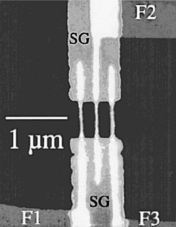
The two-layered Schottky gate pattern shown in Fig. 1 was defined by electron beam lithography on the surface of a high-mobility GaAs/Al0.33Ga0.67As heterostructure T258, 157 nm above a 2DEG. There is a 30-nm-thick layer of polymethylmethacrylate (PMMA) which has been highly dosed by an electron beam, to act as a dielectric[22] between the split gate (SG) and three gate fingers (F1, F2, and F3) so that all gates can be independently controlled.
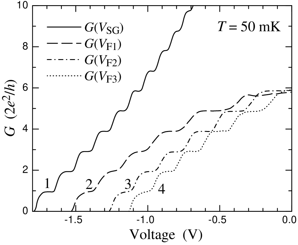
After brief illumination by a red light emitting diode, the carrier concentration of the 2DEG was m-2 with a mobility of m2/V s. The corresponding transport mean free path is m, much longer than the effective 1D channel length. Experiments were performed in a dilution refrigerator at mK and the two-terminal conductance was measured using an ac excitation voltage of V with standard phase-sensitive techniques. In all cases, a zero-split-gate-voltage series resistance () is subtracted. Two samples, at five different cooldowns, show similar characteristics, and measurements taken from one of these are presented in this paper. Trace 1 in Fig. 2 shows the conductance measurements as a function of split-gate voltage when all finger gate voltages , , and are zero.
Conductance plateaus at multiples of are pronounced (with no resonant feature superimposed on top) as expected for a clean 1D channel. When the channel is defined at V, six quantized conductance steps are observed when each one of the finger gates is swept while the others are grounded to the 2DEG as shown in traces 2–4 (Fig. 2). These experimental results demonstrate that a clean 1D channel is obtained in which impurity scattering is negligible. A lateral quantum dot was defined by applying voltages on SG, F1, and F3, while keeping F2 grounded to the 2DEG. Resonant features are observed only when large negative voltages are applied to both F1 and F3.
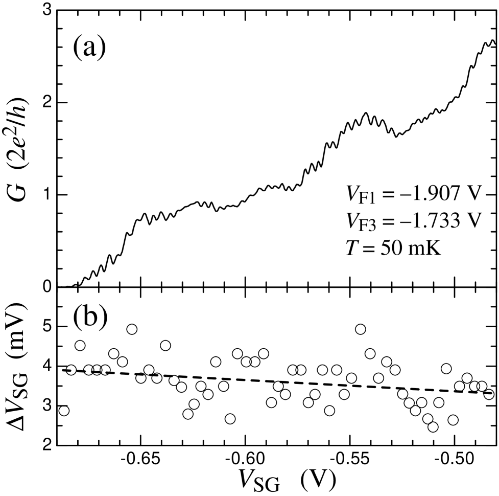
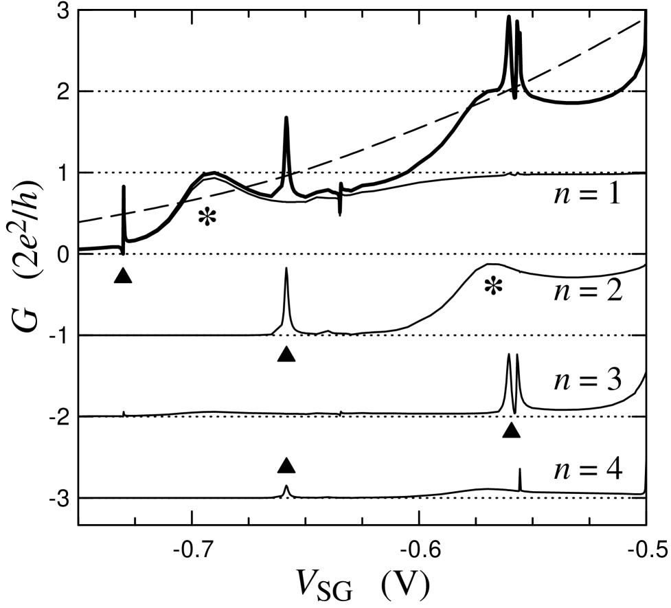
With some depletion voltage V at low-temperature, almost periodic and continuous oscillations of conductance over a wide range are observed. Typical traces of the conductance and the distance between adjacent peaks (“period”) as functions of gate voltage are shown in Fig. 3. The period and shape of the oscillations remain approximately the same within the wide range where is varied, though the background conductance changes considerably. While the oscillations at can be ascribed to Coulomb charging effects, the oscillations for are unexpected.
The observed oscillations are essentially different from the single-electron effects in older type lateral quantum dots[9, 10, 11] in which single electron tunneling peaks increase in height and decrease in width as the conductance decreases, and the period of the oscillations is well defined. The latter behaviour corresponds to the orthodox theory of Coulomb blockade.[2] In contrast to the majority of the other papers where low-temperature single-electron effects have been studied,[5, 24, 25] the trace in Fig. 3 has neither equally spaced narrow peaks nor regions of strongly suppressed conductance (Coulomb blockade) inbetween the peaks. Instead, all the oscillations in Fig. 3 are smoothed, have small amplitude , are approximately the same width, and the peak spacing fluctuates by several tens of percent.
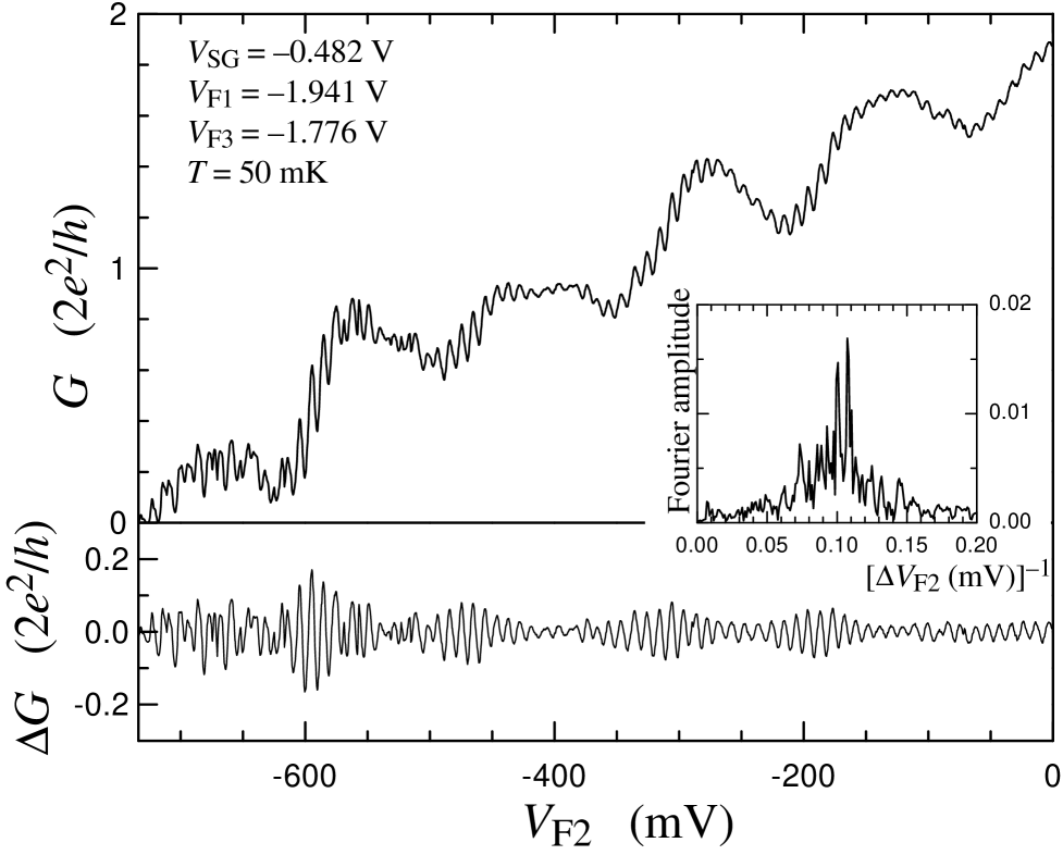
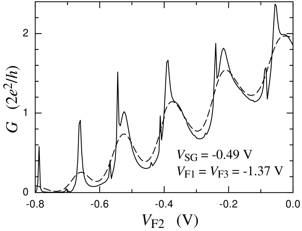
Figure 4 shows that similar oscillations are observed when the central finger gate voltage is varied, with the side gate voltage fixed. At the top of Fig. 4 the conductance is shown along with its running average (the background). The oscillations without the background, , are shown at the bottom and their Fourier spectrum is given in the inset. Noticeably, in the region V, where , the peaks should be strictly equidistant according to Coulomb blockade theory, additional beats are evident.
The observed oscillations overlay the wide maxima or steps of the conductance which appear periodically with the central finger gate voltage varied at fixed (Fig. 4) and are most likely associated with electron wave interference on the system of two barriers in the constrictions. With changing the depth of the potential well in the quantum dot the resonances move through the Fermi level one by one. Previous studies[24] have reported the observation of Coulomb oscillations superimposed on almost periodic conductance peaks at and were interpreted as Fabry-Pérot resonances due to coherent electron tunneling through the quantum dot. In our case the frequent small-amplitude oscillations penetrate to the region , where the transport is traditionally considered coherent and Coulomb charging effects are not usually observed.
Generally for , it is expected that the presence of a fully transmitted 1D channel might cause mode mixing between 1D channels in the quantum dot which should smear out charging effects. However, due to the special design and high quality of this device it is likely that there is little 1D mode mixing in the chosen range of gate voltages such that the level broadening for Coulomb oscillations is similar for both cases when and .
B Temperature evolution
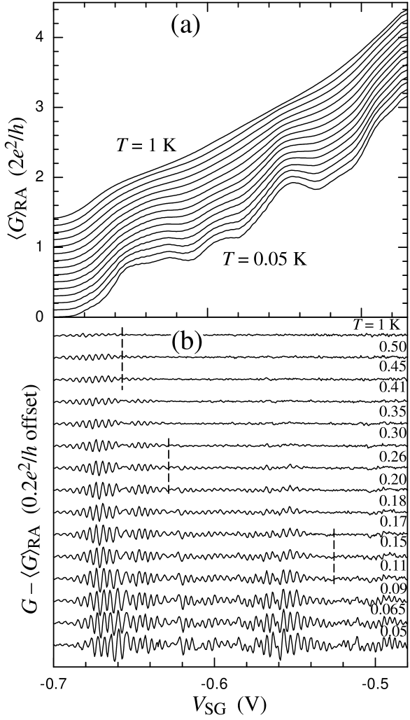
Figure 5 shows how the features in the background (a) and the oscillations (b) of the conductance of the quantum dot develop with decreasing temperature from K to mK. Consider the behaviour of the background first [see Fig. 5(a)]. At 1 K there is no conductance quantization. Only the wide shoulder at V marks out the tunneling regime of the first subband . Around two plateaus at and appear. With lowering the temperature down to 50 mK resonant features develop: plateaus transform to peaks and shoulders emerge at and . Thus, in contrast to the well-quantized ballistic conductance plateaus shown in Fig. 2, applying voltages to F1 and F3 results in conductance steps that are not as flat or well quantized.
In figure 5(b), at 1 K only a group of weak conductance oscillations within the range V are discernible. These oscillations are located at the bottom slope of the first subband and relate to the tunneling regime , so they can be ascribed, by analogy with Coulomb blockade peaks,[9, 10, 11] to Coulomb charging effects. For K a group of oscillations appear in the range V which ascend up to . Then at K oscillations at higher conductance show up for V. And finally, at K oscillations become visible when the conductance is between the second and third quantum . This division into groups of oscillations is traced down to K. Within the groups, additional modulation of the amplitude of oscillations is pronounced and correlates with the resonant features of the background conductance . Thus, each group can be characterized by the temperature at which its oscillations become visible. The fact that the frequent oscillations appear at K before the wider resonant features do at K precludes their unified interpetation by transmission resonances at coincidences of quasidiscrete levels of the dot with Fermi level. Indeed, the energy scale, i. e. critical of the frequent oscillations exceeds that of the wider features, while the resonances at the single-particle levels would have smaller energy spacing than the width of Fabry-Pérot resonances.
The level spacing estimated from Aharonov-Bohm oscillations following the method described in Ref. [26] gives eV,[18] comparable to the thermal smearing at 150 mK. On the other hand, estimating the charging energy from the critical temperature K at which the oscillations are still observed results in meV. Thus the observed oscillations are not due to resonances on single-particle levels of the dot and can be described in terms of the Coulomb charging picture where the 0D quantum confinement energy is much smaller than the Coulomb charging energy.
The most likely explanation for the frequent oscillations showing up in the region with lowering temperature is the decrease of the decay probability of the localized states in the dot via fully transmitted 1D-subbands. Increasing the temperature enhances the mixing between transmitted and closed 1D-subbands such that oscillations suppressed at (two 1D-subbands are fully transmitted), thereafter become suppressed at (1D-subband), and eventually at , where only tunneling decay of the localized states is possible.
C Gate voltage dependences of oscillations
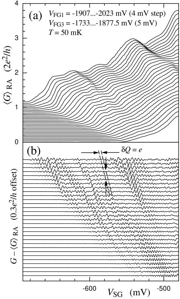
Figure 6 demonstrates how the background conductance (a) and the oscillations less the background (b) change with incremental voltage steps on the outermost finger gates at mK. One can see that the oscillations of gradually evolve with similar shape and periodicity from the region to the region , indicating their common physical origin. Since for Coulomb blockade theory holds and the oscillations are due to Coulomb charging, the observed evolution of the oscillations to serves as an experimental confirmation of the single-electron nature of all the oscillations.
From the observed Aharonov-Bohm type oscillations[18] the dot area was determined to be m2 and the number of electrons was for V, V, and V. Provided that every conductance oscillation corresponds to a change of the dot charge by , one can determine (from the total number of oscillations ) that there are still electrons within the dot at pinch-off V.
Note that the modulation of the oscillation amplitude in Fig. 6(b) allows us to trace the movement of the oscillations for different along almost parallel lines which corresponds to the conservation of the dot charge . Two such lines are shown dashed in Fig. 6(b); where both horizontal and vertical separation between them obeys the same condition . Wide stripes of amplitude modulation markedly divide the oscillations into groups in agreement with Fig. 5(b), and their slope reproduces that of the conductance threshold. Also, the groups of oscillations correlate with the locations of the resonant features of the background in Fig. 6(a).
The background conductance [see Fig. 6(a)] contains both steps and bumps which move with the conductance threshold as the finger gate voltage raises the barriers in the constrictions; these features are smeared out and completely disappear with decreasing transparency of the barriers. There are several reasons for such behaviour. Firstly, the tops of the barriers in the constrictions approach the Fermi level with a large negative voltage on the finger gates. Any small, but inevitable, asymmetry between the two constrictions on the transport properties will be enhanced, causing the height of the steps and resonant peaks of the conductance to reduce. Secondly, smearing of the features that occurs at lower negative voltages , when increases, is favoured by a widening of the constrictions over this voltage range thereby reducing the intersubband spacing there. And lastly, any decrease of the transparency of the barriers increases the electron dwell time in the dot and the role of decoherence, such that the constrictions start acting independently. The quantised coductance steps for a single constrictions smear out in this voltage regime as shown by both measurements [see Ref. [27], Fig. 2(a)] and modelling.
The condition can be used to find the capacitances between the dot and the gates of the sample. For this purpose the periods of conductance oscillations versus gate voltages were measured, mV, mV, mV, and mV. According to this the total gate-dot capacitance is estimated to be F.
III Numerical results
A Electrostatics
In order to check the correspondence between the observed period of oscillations and the change of the dot charge by one electron, and to obtain an estimate of the charging energy, we calculated the capacitance of the dot with respect to the contacts, fingers, and split gates. The electrostatic potential profile in the device was determined by solution of the 3D Poisson equation with a local 2DEG density given by the 2D Thomas-Fermi approximation assuming a boundary condition of frozen charge at the surface states and impurities. It was checked that fluctuation potential in this structure due to ionised dopants is absent due to the wide AlGaAs spacer ( nm).
The conformity of this fairly simple model to the experiment was checked by calculation of the pinch-off voltages. The calculated Fermi level meV in the 2DEG reservoirs corresponds to the measured carrier density cm-2. In the calculations the same voltage was applied to the outermost finger gates, and the central finger gate was set at zero voltage. At the channel pinches off when V (the same as in the experiment). When V the finger gates raise the potential barriers in the constrictions above the Fermi level at V (experimentally the split-gate pinches off at V when V and V). We ascribe this small difference between the calculated () and experimental () values to the fact that we do not take into account the capacitances of the finger gates with respect to the shield of the structure (we also neglect electric field lines going above the PMMA layer).
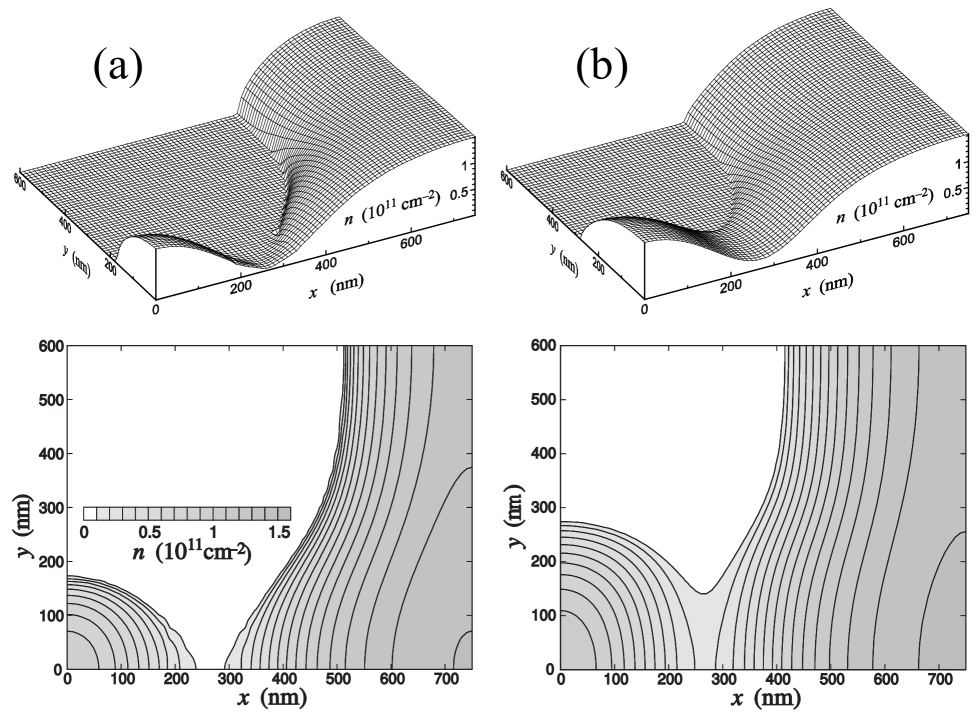
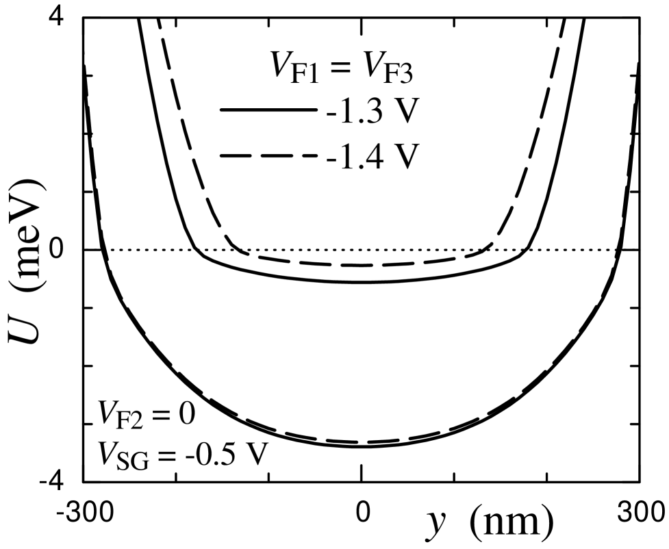
We calculated the potential profile, charge distribution and the total charge of the dot, as well as the capacitances in the range to V and to V which closely agrees with the range of experimental gate voltages specified for the traces in Figs. 3–5. These results are shown in Figure 7 which shows maps of the charge density in the quantum dot for closed and open states. With lowering the dot stretches along axis and becomes rectangular.
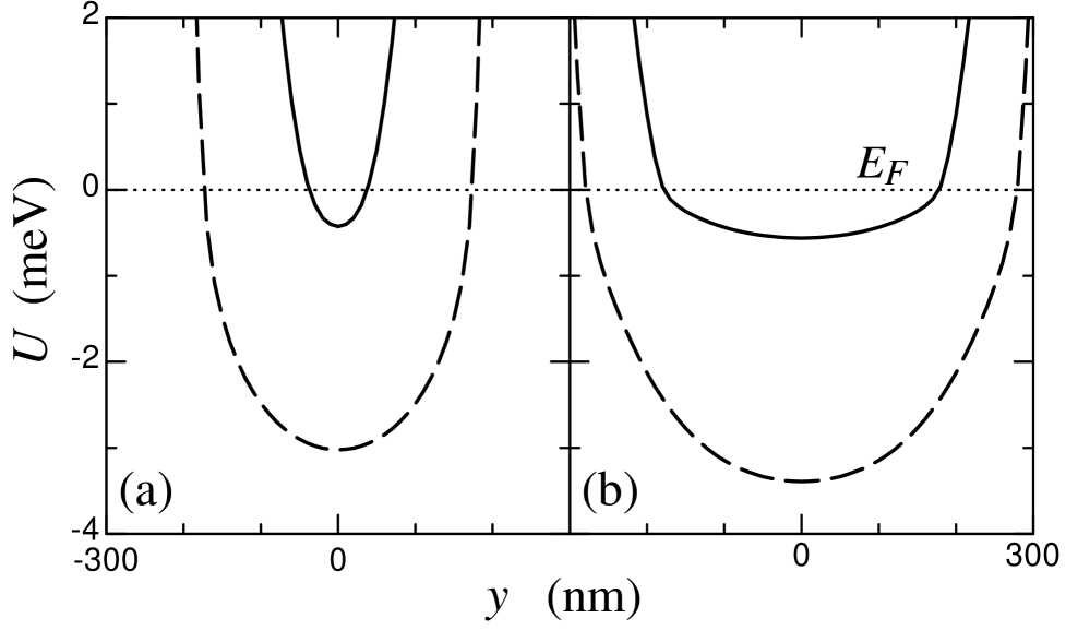
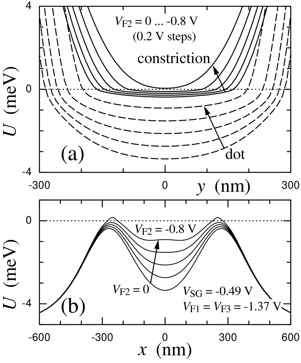
Transverse cross sections of the electrostatic potential in the 2DEG are shown in Fig. 8(a,b) for two different coordinates along the channel: in the center of the dot at , and directly beneath the finger gates at nm. By changing the voltage the dot transforms from a closed state (a) to an open state (b), with a corresponding change in the width of both the dot and the constriction. The voltage on the finger gates control both the height of the barriers and the width of the constrictions (Fig. 9) with little change in the depth of the dot. At large finger gate voltages to V and low side-gate voltages V the transverse potential profile of the constriction resembles a rectangular well (Fig. 9). With the central finger gate kept at zero voltage, the width and depth of the quantum dot were found to depend on only. It is interesting to note that the presence of zero-biased F2 makes the dot 0.5 meV deeper in energy and stabilizes its depth at meV [see Fig. 8(a,b)]. On the other hand, if the voltage on the outermost finger gates is fixed and the central finger gate voltage is varied, it mainly changes the depth of the potential in the quantum dot (Fig. 10).
The calculations show that the number of electrons in the dot changes from 80 to 140 as the side gate voltage changes from V to V (with fixed V). This change in the number of electrons corresponds to the number of oscillations observed in Fig. 3. Calculated capacitances of the dot to the gates are also close to the experimentally estimated ones and lay within the measured period variation (Table I). In calculations the capacitances demonstrated the same systematic drift with and as observed in Fig. 3(b). Thus, the conclusion that each oscillation of the conductance reflects the change of the dot charge by one electron is confirmed.
By introducing a small Fermi level difference between the dot and the 2DEG reservoirs, we calculated the capacitance of the dot with respect to both contacts as aF for an almost closed quantum dot. The capacitance is doubled when three 1D-subbands become transmitted. Thus, this capacitance is almost an order of magnitude higher than that to the gates and cannot be neglected, so the charging energy is meV, where , comparable to the thermal broadening at K. As Fig. 5 shows, near the pinch-off the conductance oscillations persist up to 1 K, in accordance with the conventional theory of Coulomb blockade. The decrease of the charging energy to 0.1 meV at , as found in the calculations of the electrostatics, should lower the limiting temperature for observing the oscillations in this range to K. Figure 5 shows that in reality the measured temperature is still 3 times smaller. This strong reduction could be caused by an enhanced decay of the localized states via two fully transmitted subbands and an increase in the intersubband mixing.
B Comparing quantum dots of different types
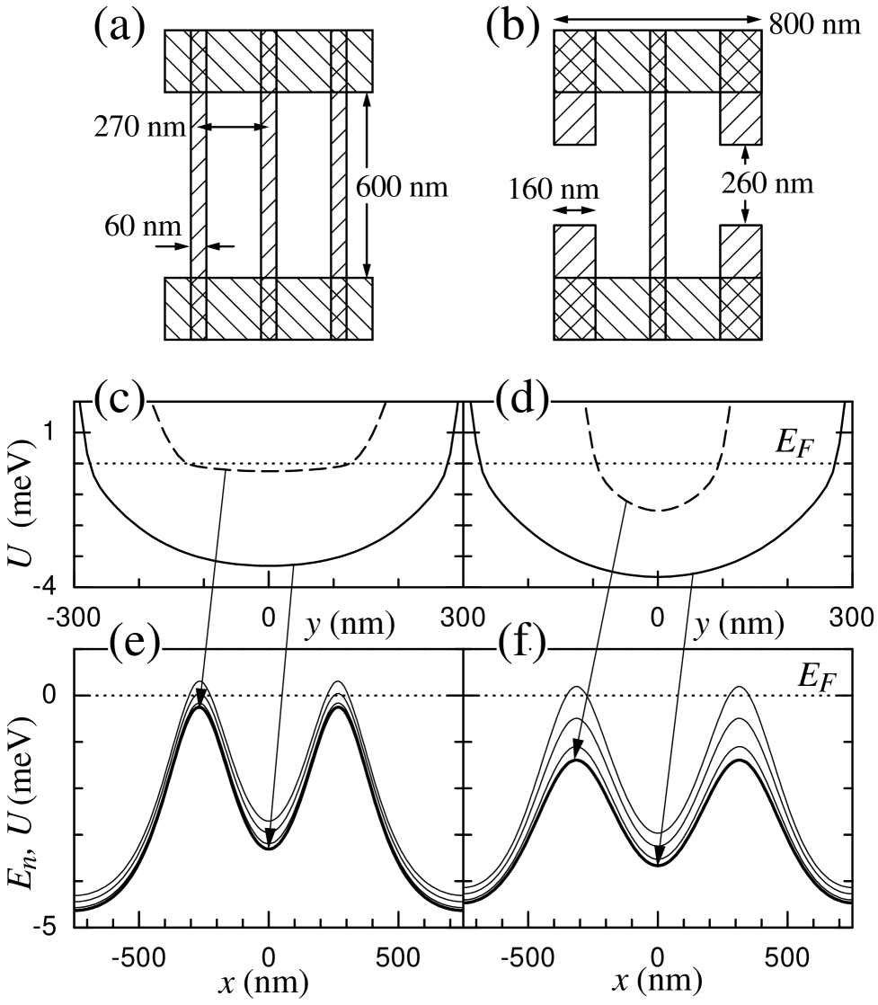
To understand the difference between the dot under study [Fig. 11(a)] and a more standard quantum dot (where the constrictions are induced by two pairs of split gates and Coulomb oscillations are observed only at ) calculations of the electrostatics were also carried out for the case in which the outermost 160 nm wide finger gates were separated by a 260 nm gap [Fig. 11(b)]. We will denote those devices as A and B, respectively. Except for the finger gates, all the parameters of devices A and B are the same. Calculated capacitances of the quantum dot in closed and open states for cases A and B are similar. The essential differences between the electrostatic potentials in the plane of the 2DEG only appear in the constrictions. In device B, the barriers in the constrictions are lower, and the transverse cross section of potential there resembles a deep and narrow parabola with energy quantum meV [Fig. 11(d)]. The quantum in the centre of the channel (the quantum dot) is 2–3 times smaller: meV. In device A the transverse potential in the constriction resembles a cut parabola [Fig. 11(c)], so the lowest 1D subbands are denser near the bottom, like that in a rectangular potential well. When the quantum dot is open for transmission via the first subband, the 1D subband spacing in device A is almost equal both inside the dot and constrictions: meV.
The energy levels of transverse quantization were determined from a solution of the Schrödinger equation for the calculated electrostatic potential by a tight-binding method. To impose zero boundary conditions for transverse motion, infinite walls were put at 600 nm from the axis of the channel. The picture of 1D-subbands shows how the subband spacing changes along the channel axis and how many subbands are open for transmission through the quantum dot at a given Fermi level.
Figures 11(e,f) show the positions of three lowest 1D-subbands for devices A and B. The Fermi level is shown by a dotted line and corresponds to zero energy. In case A, the subband spacing is almost independent of . This means that the transverse cross sections of potential in the dot and in the constrictions have the shape of the same parabola, in other words . Then the variables and in the Schrödinger equation are separated, and the motion along and directions is described by separate equations, with no mixing between different 1D subbands. Thus the transmission problem reduces to one-dimensional one.
Contrarily, in device B, where there is a gap between the finger gates, 1D subbands are not parallel and the intersubband spacing changes by 2–3 times along the channel [Fig. 11(f)]. Thus the potential has such a shape that the variables in the Schrödinger equation cannot be separated, the mixing between 1D-subbands is strong and the motion is essentially two-dimensional. Electron transmission can only be considered one-dimensional when the first subband is opening and the transmission coefficient .
These assumptions about one-dimensional transmission in device A and two-dimensional transmission in device B are supported by numerical calculations of multiple-mode transmission, as described in the next sub-section.
C Electron transmission through quantum dots
Two-dimensional transmission was calculated on the same grid in variables as the Poisson equation was solved for . Along the channel axis , energy levels in each transverse cross section and transfer matrix elements between adjacent cross sections were determined and then the multiple-mode transmission problem was solved by means of scattering -matrices. The conductance relates to the total transmission coefficient according to the Landauer formula:
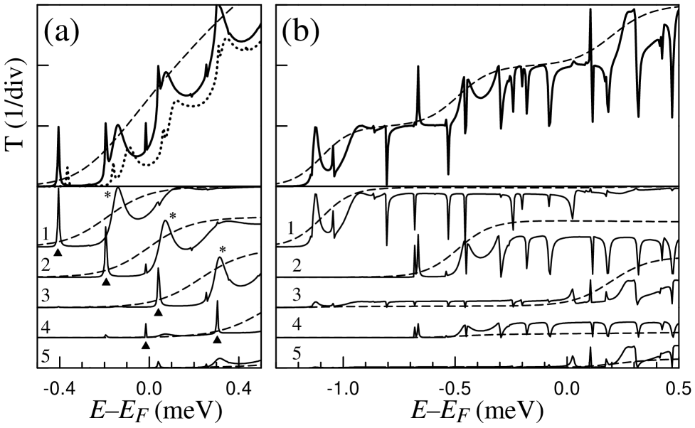
The transmission was calculated for quantum dots and single constrictions (half the quantum dot). In Fig. 12(a) plots of the Fermi energy dependence of the total transmission coefficient and its modal contributions are shown for device A ( V, V). The dashed lines show the transmission through single constrictions. When the first mode is 50% transmitted, the second mode has already reached 30% and so on. For small values of the transverse quantum meV, conductance quantization is smeared out on a single constriction, though it can occur for resonant transmission through two barriers in series.
Transmissions in the quantum dot are shown by the solid lines in Fig. 12. For device A the transmission curves for the first to third subbands resemble each other but with an offset in energy by the transverse quantum. Similar behaviour is observed in the split gate voltage dependence of the transmission in Fig. 13 which models the experimental situation shown in Fig. 3.
It is important that only a few resonant features are present in and — those are Fabry-Pérot resonances in the system of two barriers. The narrowest ones of the resonances are marked with triangles and refer to the tunneling regime of the corresponding subbands; they are smeared out in measurements and not visible in Fig. 3 since in this regime the transport is sequential rather than coherent. Contrarily, the wide resonances refer to above-barrier coherent transmission (marked with asterisks) and give rise to every next step of conductance quantization in Figs. 3–5. It seems that the conductance steps in Fig. 3 are not the property of a single barrier, but the property of the pair of barriers [see Figs. 13 and 12(a)]. The difference in the height of the barriers of meV (weak asymmetry of the structure) causes no subband mixing but reduces the conductance steps and shifts the resonances (e. g. dotted curve in Fig. 12). This asymmetry can explain the observed transformation of background conductance in Fig. 6(a).
The total transmission coefficient and modal distribution for device B are shown in Fig. 12(b) ( V, V). Dotted curves show transmission with pronounced steps for a single constriction. Because of the large subband spacing the tunneling in closed subbands is negligible. In transmission through the dot, however, the transport may go via the higher subbands due to mixing with lower open subbands. For instance, nonzero transmission via the third subband occurs due to coupling to the first subband even if the second subband is not yet transmitted. When , the transport involves more than five modes and higher modes contribute much more to the conductance than those in device A. The intersubband mixing shows up in the dependence as sharp Fano resonances due to electron scattering from the levels of the dot [Fig. 12(b)]. The dependence is similar to : transmission is one-dimensional at and already multimodal at . It should be noted that while 1D-subbands in device A become absolutely transparent () with increasing energy or , the transparency of open subbands in device B changes resonantly from 0 to 80–90% due to intersubband mixing. This can explain why charging effects are smeared out at in more standard quantum dots.
Figure 14 shows the modelled dependence of the conductance on the central finger gate voltage . The corresponding deformation of the potential in the dot and constrictions was shown in Fig. 10. The depth of the potential in the dot decreases, and the resonances due to 1D interference on the two barriers cross the Fermi level one by one. The calculated coherent transmission is shown in Fig. 14 by the solid curve from which the dashed curve without sharp peaks is obtained by smoothing. Five wide Fabry-Pérot resonances are clearly seen in the figure which are also present on the experimental curves (the background in Fig. 4).
The fact that the number of frequent oscillations in experimental curves (Figs. 3, 4) differs drastically from the number of resonant features in the calculated transmission coefficients (Figs. 13, 14) demonstrates that the observed frequent oscillations are not due to interference effects of coherent electron transmission through quasi-discrete states of the quantum dot. In the coherent regime an electron does not scatter on most levels in the absence of mode mixing. The suppression of mode mixing is a consequence of the geometry of the dot and the corresponding selected range of voltages at finger and side gates. Large negative voltage at overlaying finger gates flattens the potential across the channel so that the separation between the lowest 1D-subbands in the constrictions becomes as small as that in the dot [Fig. 11(e)]. Calculation of the transmission coefficients show that mode mixing is strengthened when the conductance rises to . This explains why the amplitude of the measured conductance oscillations and the temperature at which the oscillations vanish are reduced in this voltage range.
IV Qualitative explanation of oscillations
Based on the modelling of the electrostatics and coherent transmission we suggest the following scenario of Coulomb charging in an open quantum dot. There are three important features that the new type of dot possesses: 1) coupling between localized and transmitted subbands is suppressed; 2) coherent transmission and sequential tunneling coexist; 3) the charging energy and 1D-subband spacing in the constrictions are commensurate.
We presume that in the absence of intersubband mixing the transport in the low-transparency subbands is due to sequential tunneling with single-electron charging of the dot, resulting in the conductance oscillations (Figs. 3–6). The open subbands transmit the electrons coherently and provide a parallel background current with Fabry-Pérot resonances and quantization steps in the conductance. With each new step the single-electron charging in the opening subband ceases but it still takes place in a higher (low-transparency) subband, since the intersubband transition probability in the dot is very small at low temperature. Apparently, when the transmissions via different 1D-subbands are independent, Coulomb charging effects are manifested in a similar manner for each opening subband. That the experimentally observed conductance oscillations are continuous is due to the small spacing of transverse quantization levels in the constrictions, leading to stronger tunneling via closed subbands compared to more standard quantum dot devices.
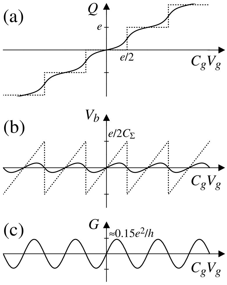
The fact that the spacing of 1D-subbands in the constrictions is approximately equal to the charging energy meV can account for the uniformity and smoothness of the observed oscillations. Indeed, electron localization and tunneling makes the charge on the dot follow the quantization, i. e. the dependence of the dot charge on gate voltage departs from linearity proportionality towards the step function [Fig. 15(a)]. From electrostatics it follows that the deviation of the dot charge from the value produces a voltage difference between the dot and reservoirs. Precise charge quantization, if it were in the Coulomb blockade regime, would lead to sawtooth modulation of between and as the value changes by [Fig. 15(b)]. However, because of the condition the transparency of the barriers in the constrictions varies strongly with changing and thus causes a periodic change of that part of the dot charge which is associated with the population of the delocalized states. As a result of continuous change of () the steps and sawteeth of the gate voltage dependences and are smoothed. Nevertheless, if the decay rate from the localized states to the transmitted ones is low these features survive even if the transport is coherent and fully transmitted subbands are present. One may imagine that charge plays the same role as the polarization charge of the Coulomb island plays in the conventional theory of Coulomb blockade. In this theory, when parameter is kept constant, the charge becomes strictly quantized at zero temperature. However, temporal fluctuations of widen the sharp features in and . In our case the situation is similar.
We have numerically found that the transparency of the quantum dot changes by when is varied by only (the bottom of the dot is raised by ). Thus, the periodic change of the embedded voltage with gate voltage results in single electron conductance oscillations in the coherent current [Fig. 15(c)].
Because the charging energy and the subband spacing in constrictions are approximately equal it follows that there is no principal difference between regimes and . In reality, besides coherent transmission there is sequential tunneling that leads to spontaneous switching between adjacent charge states of the dot. Thus for significant time is spent in a charge state with highly transparent potential barriers and similarly, for the dot often happens to be in a charge state with a low transparency of the barriers. Consequently the observed charge oscillations of the conductance appear uniformly smoothed. In addition, the amplitude and the period of such oscillations fluctuate because of the variations of the steps shape in .
On the other hand, if there is strong intersubband mixing in the quantum dot, then the dot charge undergoes large fluctuations due to coupling to the reservoirs via transmitted subbands. Then quantization of in the open quantum dot is destroyed, and the charge effects in are smeared out. Nevertheless, in submicrometer quantum dots the transverse quantum in constrictions meV is usually noticeably greater than the charging energy and pronounced Coulomb oscillations can be observed near and below the conductance treshold where the saw-like dependence of is retained.
V Conclusions
We have investigated the low-temperature properties of an open quantum dot electrostatically defined by a split gate, and overlaying narrow finger gates at zero magnetic field. Almost periodic and continuous oscillations superimposed upon ballistic conductance steps and Fabry-Pérot resonances are observed even when the conductance through the quantum dot is greater than . A direct transition of conductance oscillations for to those for is observed with decreasing barrier transparencies. The temperature dependence of the observed oscillating features for and modelling of electron transport excludes the interpretation that they are due to tunneling through single-particle confinement energy states within the dot. Calculated capacitances of the dot to the gates and reservoirs confirm the Coulomb charging nature of the oscillations. Modelling the electrostatics and electron transmission through the quantum dot show that intersubband mixing in our device is greatly reduced in comparison with more standard quantum dots. We have found that in this new design of quantum dot device the charging energy is approximately equal to the subband spacing in the barriers. Suppression of intersubband mixing and high sensitivity of barrier transparency to variations of the Fermi level in the dot made it possible to observe smoothed charged and interference effects over a wide conductance range . These results suggest that at zero magnetic field charging effects can occur in the presence of a fully transmitted 1D channel, in contrast to the current experimental and theoretical understanding of Coulomb charging.
Acknowledgements.
This work was supported by programs of Ministry of Science of Russian Federation “Physics of Solid-State Nanostructures” (grant No. 98-1102) and “Prospective Technologies and Devices for Micro- and Nanoelectronics” (No. 02.04.5.1), and by program “Universities of Russia—Fundamental Research” (No. 1994). The work at Cambridge was funded by the Engineering and Physical Sciences Research Council (EPSRC), United Kingdom. C.T.L. is grateful for financial support from National Sciences Council (grant No. 89-2112-M-002-052). O.A.T., V.A.T. and D.G.B. are grateful to Kvon Ze Don and M. V. Éntin for discussions. O.A.T. and D.G.B. thank the colleagues from Cavendish Lab., especially C. J. B. Ford, for fruitful discussions and hospitality.REFERENCES
- [1] Present address: Telecommunication Basic Research Laboratory, ETRI, Yusong P.O. Box 106, Taejon 305-600, Korea.
- [2] K. K. Likharev, IBM J. Res. Develop. 32, 144 (1988).
- [3] C. G. Smith et al., J. Phys. C 21, L893 (1988).
- [4] L. I. Glazman and R. I. Shekhter, J. Phys. Condens. Matter 1, 581 (1989).
- [5] U. Meirav, M. A. Kastner, and S. J. Wind, Phys. Rev. Lett. 65, 771 (1990).
- [6] P. L. McEuen et al., Phys. Rev. Lett. 66, 1926 (1991).
- [7] J. Weis et al., Phys. Rev. Lett. 71, 4019 (1993).
- [8] R. C. Ashoori et al., Phys. Rev. Lett. 68, 3088 (1992).
- [9] A. A. M. Staring et al., Physica (Amsterdam) 175B, 226 (1991).
- [10] L. P. Kouwenhoven et al., Z. Phys. B 85, 367 (1991).
- [11] J. G. Williamson et al., in Nanostructures and Mesoscopic Systems, edited by W. P. Kirk and M. A. Reed (Academic Press, New York, 1992), p. 255.
- [12] K. A. Matveev, Phys. Rev. B. 51, 1743 (1995).
- [13] G. Goppert et al., Phys. Rev. Lett. 81, 2324 (1998).
- [14] Y. V. Nazarov, Phys. Rev. Lett. 82, 1245 (1999).
- [15] I. L. Aleiner and L. I. Glazman, Phys. Rev. B 57, 9608 (1998).
- [16] M. Field et al., J. Phys.: Condens. Matter 6, L273 (1994).
- [17] C.-T. Liang et al., Phys. Rev. B 55, 6723 (1997).
- [18] C.-T. Liang et al., Phys. Rev. Lett. 81, 3507 (1998).
- [19] I. V. Zozoulenko and K.-F. Berggren, Phys. Rev. B 54, 5823 (1996).
- [20] T. J. Thornton et al., Phys. Rev. Lett. 56, 1198 (1986).
- [21] L. W. Molenkamp, K. Flensberg, and M. Kemerink, Phys. Rev. Lett. 75, 4282 (1995).
- [22] I. Zailer et al., Semicond. Sci. Technol. 11, 1235 (1996).
- [23] E. B. Foxman et al., Phys. Rev. B 47, 10020 (1993).
- [24] T. Heinzel et al., Europhys. Lett. 26, 689 (1994).
- [25] M. Persson et al., Phys. Rev. B 52, 8921 (1995).
- [26] R. J. Brown et al., J. Phys. Condens. Matter 1, 6291 (1989).
- [27] C.-T. Liang et al., Phys. Rev. B. 60, 10687 (1999), cond-mat/9907379.
| period of oscillations | calculated | measured |
|---|---|---|
| mV | mV | |