[
Is the Multichannel Kondo Model Appropriate to Describe the Single Electron Transistor?
Abstract
We investigate the low-temperature dynamics of single electron boxes and transistors close to their degeneracy point using renormalization group methods. We show that intermode scattering is a relevant perturbation and always drives the system to the two-channel Kondo fixed point, where the two channels correspond to the real spins of the conduction electrons. However, the crossover temperature , below which Matveev’s two-channel Kondo scenario K.A. Matveev, Phys. Rev. B 51, 1743 (1995) develops decreases exponentially with the number of conduction modes in the tunneling junctions and is extremely small in most cases. Above the ’infinite channel model’ of Ref. [6] turns out to be a rather good approximation. We discuss the experimental limitations and suggest a new experimental setup to observe the multichannel Kondo behavior.
pacs:
PACS numbers: 73.20.Dx 72.15.Qm, 71.27+a]
I Introduction
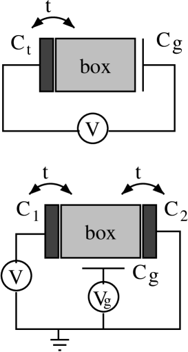
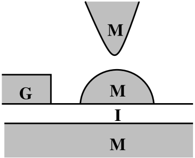
The single electron box (SEB) and the single electron transistor (SET) are basic elements of mesoscopic devices and have been studied extensively.[1, 2] Both consist of a single small metallic or semiconducting box connected to one (single electron box, or SEB) or two (single electron transistor, or SET) leads. Additionally, in the SET a gate electrode is attached to the box to control the actual charge on the dot (see Fig. 1).
The electrostatic energy of the box is well-described by the classical expression[1]
| (1) |
where denotes the capacitance of the island, is the gate capacitance, is the electric charge, stands for the gate voltage, and is the number of extra electrons on the island. For box sizes in the range the capacitance of the box can be small enough so that the charging energy associated with putting an extra electron on the island can safely be around range. Therefore, unless is a half-integer, it costs a finite energy to charge the island, and at low enough temperatures the number of electrons on the island becomes quantized and a Coulomb blockade develops provided the quantum fluctuations are not too strong. In this Coulomb blockade regime the transport through the island is suppressed.
The situation is dramatically different for dimensionless gate voltages . For the two states and become degenerate, and quantum fluctuations between the island and the leads become important. Assuming that the mean level spacing on the island is smaller than any energy scale (temperature, , etc.) two scenarios have been suggested: (a) It has been proved by Matveev[3, 4] that if the leads are connected to the island via a single conduction mode then — close to the degeneracy point and at low enough temperature — the physics of the SET (SEB) becomes identical to that of the two-channel Kondo model. Indeed, the fingerprints of the two-channel Kondo behavior have been observed recently on semiconducting single electron transistors.[5] (b) In the opposite limit one assumes that the tunneling to the island happens through an infinite number of identical modes.[6, 7] This model has been applied very successfully for the description of metallic islands.[8] The predictions of this infinite channel model are, however, very different from those of the two-channel Kondo model: the conductance of the SET, for instance, scales to zero as in the two-channel Kondo picture,[4] while it is proportional to in the infinite channel scenario.[6]
The purpose of the present paper is to treat the general case of finite conduction modes in the lead and to reconcile the apparent contradiction between the two pictures above. We show that both models capture the physical properties of the SEB (SET), however, they are appropriate in very different regimes. Carrying out a renormalization group analysis we show that there exists a crossover energy . Above , even for tunneling modes the system is well characterized by the conductance of the tunnel junctions and the SEB (SET) is satisfactorily described by the -channel model of Ref. [6]. Nevertheless, for small mode numbers pronounced deviations occur, and similar deviations appear for larger values of in the presence of pinholes in the junction, which offer a plausible explanation to the deviations observed in Ref. [8].
Below , on the other hand, the detailed structure of the tunneling matrix becomes important: At very low only a single conductance mode dominates the physics and a two-channel Kondo effect develops. Unfortunately, in most situations (and thus the Kondo temperature ) turns out to be extremely small, and the two-channel Kondo physics cannot be observed. In fact, very special experimental setups are needed to observe the two-channel Kondo behavior, as we shall discuss it in detail in our concluding section.
The paper is organized as follows: In Sec. II we describe the models applied. Secs. III and IV are devoted to the analysis of the single electron box and the single electron transistor, respectively. Finally, in Sec. V we discuss the possibility of experimental observations of the low-energy Kondo-like behavior and summarize our conclusions.
II The Models
A Hamiltonian of the SEB
For the sake of simplicity, let us first concentrate on the single electron box and generalize our results to the SET later on. Usually, the lead is described by means of independent non-interacting one-dimensional electron modes:
| (2) |
where crates an electron on the box with spin , mode index and energy . (Note that to avoid confusion, we do not follow the usual terminology and use deliberately the expression conduction mode instead of the wording ’conductance channels’, more frequent in the literature.)
In the present work we assume that the level spacing at the island is much smaller than any energy scale in the problem, and therefore these discrete levels may be represented as a single particle continuum on the island. This assumption is crucial to obtain the Kondo physics discussed in this paper, since the level spacing provides an infrared cut-off which ultimately kills the logarithmic singularities and the Kondo effect. Based on these assumptions we express the Hamiltonian of the island as[1]
| (3) | |||||
| (4) |
In Eq. (4) we assumed independent modes on the box,[9] and defined the number of electrons on the island as
| (5) |
where the symbol denotes normal ordering.
As usually, in Eq. (4) we implicitly used the assumption that the collective charge excitations decouple from the single particle excitations[2] and that the electron-electron interaction can be fully taken into account by the classical Coulomb interaction term. The validity of this approximation relies heavily on the fact the collective charge excitations relax extremely fast compared to all other time scales involved.
The coupling of the box to the lead is described by a standard tunneling Hamiltonian:
| (6) |
where we neglected the energy dependence of the elements of the tunneling matrix
It is very important that the tunneling is diagonal in the spin indices, however, it is generally non-diagonal in the mode indices. As we shall see later, the twofold spin degeneracy is the basic origin of the very low-temperature two-channel Kondo effect.[3] Once magnetic field is applied the symmetry between spin up and spin down conduction electrons is broken, and the system flows to the single channel Kondo fixed point.
The tunneling Hamiltonian of the SET differs only slightly from that of the SEB. In this case there are two leads that are connected to the island. However, as first shown by Averin and Nazarov,[10] at temperatures larger than the level spacing coherent processes connecting the two leads are strongly suppressed. Therefore, one can formally separate from each-other those single particle states on the island which participate in the tunneling from the first and the second lead, respectively.[4] These tunneling processes are then only correlated by the very fast Coulomb interaction which allows for the presence of only one excess electron on the island.
Thus for the SET the effective Hamiltonian of the island becomes[4]:
| (7) | |||||
| (8) | |||||
| (9) |
where the indices and refer to single particle states participating in the tunneling from the first and second leads, respectively, and the number operators and are defined similarly to Eq. (5).
The tunneling Hamiltonian of the SET reads:
| (10) |
where the index refers to the two junctions. For the sake of simplicity, we assumed that the number of modes in the two leads ( and ) and the number of tunneling modes on the island ( and ) is identical for both junctions( and ). This simplification does not modify our results because the two tunneling matrices and are assumed to be completely uncorrelated.
In the following we focus to the vicinity of the degeneracy points, . As already mentioned in the introduction at these gate voltages the charge states and become degenerate and quantum fluctuations dominate. For temperatures (energy scales) below the charging energy one can safely project out all the other charging states, represent the two states as two states of a pseudospin , and rewrite the tunneling part of SEB Hamiltonian in the following form:
| (11) | |||||
| (12) |
where the ’orbital pseudospins’ indicate the position of an electron and couple to , denote Pauli matrices, and the index takes values ( and ). The effective field measures the distance from the degeneracy point, with .
For the SET Eq. (11) gets modified in that the two leads provide two conduction electron ’channels’ () coupled to the charge pseudospin:
| (13) |
Note that the ’channel’ label has a role essentially different from that of the real spin of the electrons: While there is a full SU(2) symmetry associated to the latter, the former is merely a conserved quantity (corresponding to a symmetry only).
In the formulation above the case corresponds to Matveev’s two-channel Kondo model,[3] while in the limit and we recover the infinite channel model[6] mentioned in the Introduction. Obviously, both limits are somewhat specific: In many realistic systems and the first approximation seems to be inadequate. The second approximation, on the other hand, contains an artificial symmetry: There is no reason for the tunneling matrix element to be diagonal in the mode indices at all, and even more to have identical matrix element in each tunneling mode. In fact, any defect, roughness, etc. present in a real junction will produce cross-channel tunneling, and even the simplest models of a perfect tunnel junction with give different tunneling eigenvalues for the different tunneling modes. The philosophy behind this second approach is that the only physically relevant parameter is the conductance of the junction and therefore the artificial symmetry introduced has no effect. As we shall see, this philosophy is only partially justified: cross-mode tunneling — breaking this artificial symmetry — is in reality a relevant perturbation and leads the system ultimately to the two-channel Kondo fixed point.
III Perturbative scaling analysis of the SEB
It has been shown longtime ago that the Hamiltonian of Eq. (11) generates logarithmic singularities when perturbation theory in the tunneling amplitude is developed.[3] To deal with these logarithmic singularities one has to sum up the perturbation series up to infinite order. The easiest way to do this is by constructing the renormalization group (RG) equations. Fortunately, this straightforward but rather tedious calculation can be avoided by rewriting the Hamiltonian (11) in the following form:
| (14) |
and observing that Eq. (14) is formally identical to the Hamiltonian of a non-commutative two-level system.[11] The indices and in Eq. (14) take the values , the ’s denote Pauli matrices (), and the ’s can be written in a block matrix notation as
| (17) | |||
| (20) | |||
| (23) |
where we introduced the tensor notation . The and Hermitian matrices and vanish in the bare Hamiltonian, but they are dynamically generated under scaling. They correspond to charging state dependent back scattering off the tunnel junction:
| (24) | |||||
| (25) |
The scaling equations of the two-level system have been first derived in Ref. [12] and its possible fixed points and their stability have been carefully analyzed in Ref. [13]. Using this mapping we can easily construct the RG equations for the SEB:
| (26) | |||||
| (27) | |||||
| (28) | |||||
| (29) |
Here we introduced the scaling variable and defined dimensionless couplings as (and similarly, , and ) with () the density of states at the Fermi energy in mode (mode ) of the box (lead).
The scaling equation for the effective field can be obtained from that of the splitting in the two-level system problem:
| (30) |
These scaling equations are appropriate provided , otherwise the perturbative RG breaks down. They must be solved with the initial condition and . Away from the degeneracy point the “magnetic field”, i.e. the deviation from the degeneracy point is a relevant perturbation, and the scaling must be cut off at an energy scale determined selfconsistently from the condition .
Up to logarithmic accuracy, the conductivity can then be expressed in terms of the scaled dimensionless tunneling rate as
| (31) |
where denotes a universal conductance unit.
The analogues of Eqs. (27-29) have been analyzed very carefully in Refs. [13], where it was shown by means of a systematic expansion ( being the spin of the electrons) that they have a unique stable fixed point, identical to the two-channel Kondo fixed point. At this latter two orbital quantum numbers prevail, and the others become irrelevant. In the present context this statement means that there will be a unique ’effective tunneling mode’ in the lead (it is some combination of the original tunneling modes in the lead), and another unique ’tunneling mode’ in the box (also a linear combination of the original modes in the box): The effective Hamiltonian of the model at the degeneracy point corresponds to tunneling between these two modes only, and all the other modes can be neglected. This theorem therefore justifies the use of Matveev’s effective model at very low temperatures even if the number of modes in the lead or the box is larger than one.
However, as we show now, the temperature , below which the two channel Kondo behavior appears turns out to be extremely small in most cases. To see this let us consider a tunneling junction with a rough tunneling surface, and a dimensionless conductance . Obviously, in this case the matrix elements scale as so that , and they have random sign or phase relative to each-other. The occupation dependent back scatterings and are generated by Eqs. (28) and (29), and their typical matrix elements can easily be estimated to be of order . Therefore, the first two terms in Eq. (27) can be estimated to be smaller than , while the matrix elements of the last term are dominated by the term proportional to and are of order . Thus for large enough one can simply substitute and the scaling equations reduce to:
| (32) |
Multiplying this equation by and taking its trace we finally arrive at the scaling equation:
| (33) |
which is identical to the one obtained in Ref. [6] using the -channel model. The scaling equation for the effective field can also be expressed in terms of the dimensionless conductance:
| (34) |
The above two scaling equations can readily be integrated to obtain:
| (35) | |||
| (36) |
Obviously, in this approximation the physics of the SEB is completely characterized by the effective field and the conductance of the junction, and the details about the specific structure of the junction or the tunneling amplitudes are unimportant.
It is easy to estimate the crossover scale below which this approximation breaks down. The scaling towards the two-channel Kondo fixed point is generated by the second order ’coherence’ terms in Eqs. (27-29), while the third order terms tend to reduce all couplings to zero. Therefore the scale is determined by the condition that the second and third order terms in Eqs. (27-29) be of the same order of magnitude, giving . Replacing Eq. (35) by its asymptotic form we finally obtain
| (37) |
where is a constant of the order of unity. In view of the experimental values of , this scale is extremely small for , which justifies the use of the -channel model in many experimental setups.
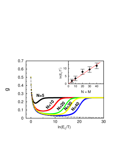
In Figs. 2 and 3 we show the typical scaling of for various and values, obtained by solving Eqs. (27-29) numerically. While in the Figures the initial hopping amplitudes have been generated completely randomly, similar results have been obtained when we used simple model estimates for the ’s. Eq. (35) approximates very nicely the conductance above even for rather small channel numbers. Below , however, the conductance starts to increase until it reaches its fixed point value . In the inset we show that the scale decreases exponentially with the number of modes in agreement with Eq. (37).
IV Discussion of the SET
To derive the scaling equations for the SET we repeated the derivation of the scaling equations of the two-level system with a generalized version of the interaction Hamiltonian (14). Here we only quote the results.
The scaling equations become:
| (38) | |||||
| (39) | |||||
| (40) | |||||
| (41) | |||||
| (42) |
Similarly to the SEB, the ’incoherent’ scaling equations can be obtained by dropping all second order ’coherent’ terms in the equations above. In this way we obtain for the dimensionless conductances and of the two junctions and the effective field the following scaling equations:
| (43) | |||||
| (44) | |||||
| (45) |
These equations can be readily solved to give:
| (46) | |||
| (47) | |||
| (48) |
Thus in this approximation the only effect of the presence of several leads is to replace the dimensionless conductance in the denominator of Eqs. (35) and (36) by the parallel conductance of all junctions attached to the island.
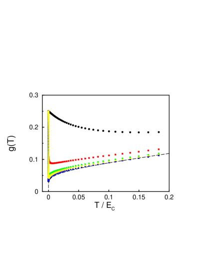
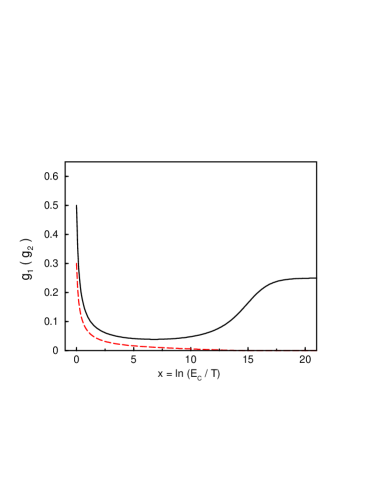
In Fig. 4 we show the conductance calculated from the solution of the full scaling equations Eq. (40-42) for conduction modes. Initially, both conductances follow Eqs. (47). However, at a temperature a single conduction mode prevails in one of the junctions and starts to induce the two-channel Kondo effect. The conductance of this junction approaches a universal value[14] characteristic to the two-channel Kondo fixed point while the resistivity of the other junction is suppressed to zero below this temperature. Since the tunneling between the island and this latter lead is an irrelevant operator of dimension and therefore its conductance scales as , the total conductance of the device at the degeneracy point scales as , in agreement with Matveev’s result. Note that the conductance of the other junction is universal, i.e. independent of the number of modes in the junction.
V Conclusions
In the present work we studied in detail the physics of the single electron box and the single electron transistor close to their degeneracy points using renormalization group methods. In particular, we investigated the effect of cross-mode scattering and showed that this is a relevant perturbation, and drives the system towards a stable two-channel Kondo fixed point, a prototype of non-Fermi liquid fixed points. At very low temperatures we recover Matveev’s mapping to the two-channel Kondo model:[3, 4] In this case at very low temperatures the system dynamically selects a single mode on the box and another one on one of the leads, and all the other modes become irrelevant. This fixed point has an symmetry,[15] where the first symmetry is generated dynamically and is connected to the structure of the effective tunneling Hamiltonian, while the second symmetry is associated to the real spin of the electrons and is responsible for the non-Fermi liquid behavior. The symmetry is simply due to charge conservation.
Due to this two-channel Kondo fixed point the linear coefficient of the specific heat and the capacitance of the SET diverge logarithmically at the degeneracy point, , while the resistivity of the device diverges as .[4]
However, as our detailed analysis demonstrates, if the number of tunneling modes is larger than one, then a new small energy scale enters into the problem, with the total number of tunneling modes. Above this scale coherent processes leading to the Kondo physics can be neglected, and the properties of the system are very well described solely in terms of the conductances of the various junctions. Neglecting the aforementioned coherent terms we were able to re-derive the equations of Ref. [6], and generalize them for the case of SET.
At this point we have to make an important remark. Our results for the two-channel Kondo fixed point rely heavily on the fact that the electrons at temperatures larger than the level spacing on it can hardly travel coherently from one junction to another.[10, 4] Neglecting this coherent process then one of the SET conductances scales to zero and so does the total conductance of the SET at the degeneracy point.[4]
Apart from inelastic scattering, the main origin of this loss of coherence is in the random scattering from the wall of the island and the impurities on it. Any model assuming the existence of consecutive coherent tunneling events between different leads gives an essentially different, and very likely in most situations unphysical result at very low temperatures. Indeed, repeating our analysis for the model used in Ref. [7] we find that at both tunnel junctions of the SET have a finite conductance at the degeneracy point, and thus the total conductance of the SET also remains finite even at zero temperature. This result is essentially different from the one obtained by Matveev[3, 4] or the calculations presented here, where coherent tunneling processes between different leads are excluded.
The difference between these two approximations becomes even more striking for the case of an -fold degenerate multi-degeneracy points of a multi-dot system. In this case, neglecting the above-mentioned coherent tunneling between different leads, we find that the low-temperature physics is again described by the two-channel Kondo model. In the opposite case, however, the system would scale to another non-Fermi liquid fixed point, the Coqblin-Schrieffer fixed point.
How and at what energy scale the crossover between these two behaviors happens, seems to be presently an open question, which can only be answered by somehow incorporating more details about the scattering on the impurities and the energy and spatial dependence of the tunneling matrix elements.
Because of the exponential dependence of , even a relatively small number of tunneling modes leads to an extremely small and renders the non-Fermi liquid behavior in most cases inaccessible for the experimentalists. To observe the 2-channel Kondo behavior one can use semiconducting or metallic quantum boxes.
Semiconducting devices have the advantage that using suitable gate electrodes one can realize the idealistic case of a single mode contact, and therefore can be achieved. There is a serious difficulty, however, since one should keep large enough in order to have a measurable Kondo temperature while having a small level spacing on the island, the latter playing the role of an infrared cutoff for the Kondo physics. The former requirement immediately sets an upper limit on the size of the box , and therefore a lower limit on the mean level spacing , where we assumed a two dimensional electron gas with effective mass . This means that even if one manages to build a semiconducting device with a Kondo temperature in the measurable range, the level spacing will be too large to observe the two-channel Kondo behavior in detail. Indeed, even in the very recent experiments of Ref. [5] the ratio was in the range , and consequently only some fingerprints of the two-channel Kondo behavior could have been observed. For smaller islands would become larger, however, the ratio would get even worse. Therefore there seems to be no hope to investigate the two-channel Kondo behavior with semiconducting devices more in detail.
The other possibility is to prepare metallic boxes. Since these metallic boxes are three dimensional objects and (unlike semiconducting devices with ), metallic grains of the size of only may have quite large , and very small mean level spacing on the other hand. Indeed, using STM devices to tunnel into metallic drops[16] it was possible to observe the Coulomb blockade even at room temperature.[17]
The difficulty in this case is connected to the preparation of the junctions. As emphasized earlier, one needs practically single mode or at most few mode junctions in order to have large enough, which requires atomic size contacts/junctions. To establish such a junction we propose the experimental setup illustrated in Fig. 5. In the suggested experiment a metallic electrode is covered by a thin insulating layer, and a metallic drop is deposited on the top of it. The atomic size contacts can be formed by plugging an STM needle into one of the drops and then gently pulling it out of it.[18] An additional gate electrode should be built in the vicinity of the drop to control the charging of the island. The two-channel Kondo effect would then show up in the gate voltage dependence of the conductance through the island.
The biggest difficulty in the experiment above is to establish a stable contact, so that one has enough time to tune the drop to its degeneracy point and carry out the measurement. It would be much more advantageous to use nanotechnology to build atomic size contacts instead of using an STM, a possibility which may be not too far away any more.
The authors are grateful to G. Schön, and M. Devoret for valuable discussions. This research has been supported by the U.S - Hungarian Joint Fund No. 587, grant No. DE-FG03-97ER45640 of the U.S DOE Office of Science, Division of Materials Research, and Hungarian Grant Nr. OTKA T026327, OTKA F29236, and OTKA T029813.
REFERENCES
- [1] For a review on single electron tunneling see e.g.: Single Charge Tunneling, Vol. 294 of NATO Advanced Studies Institute, Series B: Physics, edited by H. Grabert and M.H. Devoret (Plenum, New York. 1992).
- [2] M. Devoret in Les Houches Summer School on Mesoscopic Quantum Physics, edited by E. Akkermans et al. (North-Holland, Amsterdam, 1995).
- [3] L.I. Glazman and K.A. Matveev, Sov. Phys. JETP 71, 1031 (1990); K.A. Matveev, ibid. 72, 892 (1991).
- [4] K.A. Matveev, Phys. Rev. B 51, 1743 (1995); A. Furusaki and K. A. Matveev, Phys. Rev. B 52, 16676 (1995).
- [5] D. Berman, N.B. Zhetinev, and R.C. Ashoori, Phys. Rev. Lett. 82, 161 (1999).
- [6] G. Falci, G. Schön, G.T Zimanyi, Phys. Rev. Lett. 74, 3257 (1995).
- [7] J. König, H. Schöller, and G. Schön, Phys. Rev. B 58, 7882 (1998).
- [8] Exp.: P. Joyez et al., Phys. Rev. Lett. 79, 1349 (1997).
- [9] In reality, any roughness of the surface or non-ideal geometry results in the mixing of these idealistic modes. This can be taken into account through a potential scattering term in the Hamiltonian, and as far as the mean free path of the electrons is larger or comparable to the width of the junction does not influence the results obtained.
- [10] D. V. Averin and Yu. V. Nazarov, Phys. Rev. Lett. 65, 2446 (1990).
- [11] For reviews see D.L. Cox and A. Zawadowski Adv. Phys. 47, 599 (1998); G. Zaránd and K. Vladár Int. Journal of Mod. Phys. B 11, 2855 (1997).
- [12] G. Vladár and A. Zawadowski, Phys. Rev. B 28, 1564, 1582, 1596 (1983).
- [13] G. Zaránd, Phys. Rev. B 51, 273 (1995); G. Zaránd and K. Vladár, Phys. Rev. Lett. 76, 2133 (1996).
- [14] According to the non-perturbative calculations of Ref. [4] the two-channel Kondo fixed point corresponds to perfect transmission in a single mode, i.e. . Strictly speaking, this value of the conductance is out of the reach of the weak coupling theory developped in this paper, which only predicts that the conductance is of the order of one.
- [15] Actually, the symmetry at the fixed point is , which is somewhat larger.
- [16] R. Wilkins, E. Ben-Jacob, and R.C. Jaklevic, Phys. Rev. Lett. 63, 801 (1989).
- [17] C. Schönenberger, H. van Houten and C.W.J. Beenakker, Physica B 189, 218 (1993).
- [18] L. Olesen et al., Phys. Rev. Lett. 72, 2251 (1994).