Quantum transport in ballistic conductors: evolution from conductance quantization to resonant tunneling
Abstract
We study the transport properties of an atomic-scale contact in the ballistic regime. The results for the conductance and related transmission eigenvalues show how the properties of the ideal semi-infinite leads (i.e. measuring device) as well as the coupling between the leads and the conductor influence the transport in a two-probe geometry. We observe the evolution from conductance quantization to resonant tunneling conductance peaks upon changing the hopping parameter in the disorder-free tight-binding Hamiltonian which describes the leads and the coupling to the sample.
pacs:
PACS numbers: 73.23.AdMesoscopic physics [1] has changed our understanding of transport in condensed matter systems. The discovery of new effects, such as weak localization [2] or universal conductance fluctuations, [3] has been accompanied by rethinking of the established ideas in a new light. One of the most spectacular discoveries of mesoscopics is conductance quantization (CQ) [4, 5] in a short and narrow constriction connecting two high-mobility (ballistic) two-dimensional electron gases. The conductance of these quantum point contacts as a function of the constriction width has steps of magnitude . New experimental techniques have allowed observation of similar phenomena [6] in metallic point contacts of atomic size. The Landauer formula [7] for the two-probe conductance
| (1) |
has provided an explanation of the stepwise conductance in terms of the number of transverse propagating states (“channels”) at the Fermi energy which are populated in the constriction. Here is the transmission matrix, transmission eigenvalues and is the conductance quantum. In the ballistic case is , or equivalently is . Further studies have explored CQ under a range of conditions. [8] They include geometry, [9, 10] scattering on impurities, [11] temperature effects, and magnetic field.
In this paper we study the influence of the attached leads on ballistic transport (, being elastic mean free path, being the system size) in a nanocrystal. We assume that in the two-probe theory an electron leaving the sample does not reenter the sample in a phase-coherent way. This means that at zero temperature phase coherence length is equal to the length of the sample . In the jargon of quantum measurement theory, the leads act as a “macroscopic measurement apparatus”. Our concern with the influence of the leads on conductance is therefore also a concern of quantum measurement theory. Recently, the effects of a lead-sample contact on quantum transport in molecular devices have received increased attention in the developing field of “nanoelectronics”. [12] Also, the simplest lattice model and related real-space Green function technique are chosen here in order to address some practical issues which appear in the frequent use of these methods [1] to study transport in disordered samples. We emphasize that the relevant formulas for transport coefficients contain three different energy scales (corresponding to the lead, the sample, and the lead-sample contact), as discussed below.
In order to isolate only these effects we pick the strip geometry in the two-probe measuring setup shown on Fig. 1.

The nanocrystal (“sample”) is placed between two ideal (disorder-free) semi-infinite “leads” which are connected to macroscopic reservoirs. The electrochemical potential difference is measured between the reservoirs. The leads have the same cross section as the sample. This eliminates scattering induced by the wide to narrow geometry [10] of the sample-lead interface. The whole system is described by a clean tight-binding Hamiltonian (TBH) with nearest neighbor hopping parameters
| (2) |
where is the orbital on the site . The “sample” is the central section with sites. The “sample” is perfectly ordered with . The leads are the same except . Finally, the hopping parameter (coupling) between the sample and the lead is . We use hard wall boundary conditions in the and directions. The different hopping parameters introduced here have to be used to get the conductance at Fermi energies throughout the whole band extended by the disorder, [13] i.e. . Thus, one has to be aware of the conductances we calculate in our analysis when engaging in such studies.
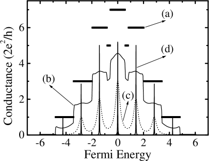
Our toy model shows exact conductance steps in multiples of when . This is a consequence of infinitely smooth (“ideally adiabatic” [9]) sample-lead geometry. Then we study the evolution of quantized conductance into resonant tunneling conductance while changing the parameter of the leads as well as the coupling between the leads and the conductor . An example of this evolution is given on Fig. 2. The equivalent evolution of the transmission eigenvalues of channels is shown on Fig. 3. A similar evolution has been studied recently in one-atom point contacts. [14]
The non-zero resistance is a purely geometrical effect [15]
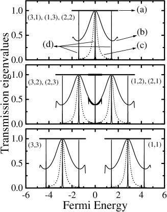
caused by reflection when the large number of channels in the macroscopic reservoirs matches the small number of channels in the lead. The sequence of steps ( multiples of as the Fermi energy is varied) is explained as follows. The eigenstates in the leads, which comprise the scattering basis, have the form at atom , with energy , where is the lattice constant. The discrete values and define subbands or “channels” labeled by , where runs from to and runs from to . The channel is open if lies between the bottom of the subband, , and the top of the subband, . Because of the degeneracy of different transverse modes in 3D, several channels open or close at the same energy. Each channel contributes one conductance quantum . This is shown on Fig. 2 for a sample with cross section where the number of transverse propagating modes is . In the adiabatic geometry, channels do not mix, i.e. the transmission matrix is diagonal in the basis of channels defined by the leads.
We compute the conductance using the expression obtained in the framework of Keldysh technique by treating the coupling between the central region and the lead as a perturbation. [16] This provides the following, Landauer-type, formula for the conductance in the non-interacting system
| (3) | |||||
| (4) |
Here , are matrices whose elements are the Green functions connecting the layer and of the sample. Thus only the block of the whole matrix is needed to compute the conductance. The positive operator is the counterpart of the spectral function for the self-energy introduced by the left lead. It “measures” the coupling of the open sample to the left lead ( is equivalent for the right lead).The Green operator is defined as the inverse of including the relevant boundary conditions. Instead of inverting the infinite matrix we invert only defined on the Hilbert space spanned by orbitals inside the sample [16]
| (5) |
where is TBH for the sample only. This is achieved by using the retarded self energy introduced by the left and the right lead. In site representation Green operator is a Green function matrix . Equation (5) does not need the small imaginary part necessary to specify the boundary conditions for the retarded or advanced Green operator because the lead self-energy adds a well defined imaginary part to . This imaginary part is related to the average time an electron spends inside the sample before escaping into the leads. The self-energy terms have non-zero matrix elements only on the edge layers of the sample adjacent to the leads. They are given [1] in terms of the Green function on the lead edge layer and the coupling parameter
| (7) | |||||
where is the pair of sites on the surfaces inside the sample which are adjacent to the leads ( or ). The self-energy in the channel is given by
| (8) |
for . We use the shorthand notation , where is the energy of quantized transverse levels in the lead. In the opposite case we have
| (9) |
In order to study the conductance as a function of two parameters
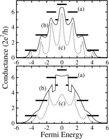
and we change either one of them while holding the other fixed (at the unit of energy specified by ), or both at the same time. The first case is shown on Fig. 2 and Fig. 4 (upper panel), while the second one on Fig. 4 (lower panel). The conductance is depressed in all cases since these configurations of hopping parameters effectively act as a barriers. There is a reflection at the sample-lead interface due to the mismatch of the subbands in the lead and in the sample when differs from . This demonstrates that adiabaticity is not necessary condition for CQ. In the general case, each set of channels which have the same energy subband is characterized by its own transmission function . When the coupling is small a double-barrier structure is obtained which has a resonant tunneling conductance. The electron tunnels from one lead to the other via discrete eigenstates. The transmission function is composed of peaks centered at , where is now quantized inside the sample, i.e. runs from to . The magnitude and width of peaks is defined by the rate at which an electron placed between barriers leaks out into the lead. These rates are related to the level widths generated through the coupling to the leads. In our model they are energy (i.e. mode) dependent. For example at seven transmission eigenvalues are non-zero (in accordance with open channels on Fig. 3) and exactly at three of them have and four . Upon decreasing further all conductance peaks, except the one at , become negligible. Singular behavior of at subband edges of the leads was observed before. [11]
It is worth mentioning that the same results are obtained using a non-standard version of Kubo-Greenwood formula [17] for the volume averaged conductance
| (11) | |||||
| (12) |
where is the component of the velocity operator. This was originally derived for an infinite system without any notion of leads and reservoirs. The crucial non-standard aspect is use of the Green function (5) in formula (4). This takes into account, through lead self-energy (7), the boundary conditions at the reservoirs. The reservoirs are necessary in both Landauer and Kubo formulations of linear transport for open finite systems. They provide thermalization and thereby steady state of the transport in the central region. Semi-infinite leads [18] are a convenient method to model the macroscopic reservoirs. When employing the Kubo formula (4) one can use current conservation and compute the trace only on two adjacent layers inside the sample. To get the correct results in this scheme in Eq. (4) should be replaced [13] by a lattice constant .
In the quantum transport theory of disordered systems the influence of the leads on the conductance of the sample is understood as follows. [19] An isolated sample has a discrete energy spectrum. Attaching leads necessary for transport measurements will broaden energy levels. If the level width due to the coupling to leads is larger than the Thouless energy , ( being the diffusion constant) the level discreteness is unimportant for transport. For our case of ballistic conduction, is replaced by the inverse time of flight . In the disordered sample where , varying the strength of the coupling to the leads will not change the transport coefficients. In other words, the intrinsic resistance of the sample is much larger than the resistance of the lead-sample contact. [20] In the opposite case, discreteness of levels becomes important and the strength of the coupling defines the conductance. This is the realm of quantum dots [21] where weak enough coupling can make the charging energy of a single electron important as well. Changing the properties of the dot-lead contact affects the conductance, i.e. the result of measurement depends on the measuring process. The decay width of the electron emission into one of the leads is determined by transmission probabilities of channels through the contact and mean level spacing. [19] This means that mean dwell time inside our sample depends on both and . Changing the hopping parameters will make greater than the time of flight . Thus we find that ballistic conductance sensitively depends on the parameters of the dephasing environment (i.e. the leads).
In conclusion, we have studied the transport properties of a ballistic nanocrystal placed between two semi-infinite leads in the simplest strip geometry. We observe extreme sensitivity of the conductance to changes in the hopping parameter in the leads as well as the coupling between the leads and the sample. As can be easily anticipated, the conductance evolves from perfect quantization (as a result of an ideal adiabatic geometry) to resonant tunneling. Nevertheless, it is quite amusing that vastly different are obtained between these two limits (e.g. Fig. 4). The results are of relevance for the analogous theoretical studies in disordered conductors as well as in the experiments using clean metal junctions with different effective electron mass throughout the circuit.
This work was supported in part by NSF grant no. DMR 9725037. We thank I. L. Aleiner for interesting discussions.
REFERENCES
- [1] S. Datta, Electronic transport in mesoscopic systems (Cambridge University Press, Cambridge, 1997).
- [2] L. P. Gor’kov, A. I. Larkin, D. E. Khmel’nitskii, Pis’ma Zh. Eksp. Teor. Fiz. 30, 248 (1979) [JETP Lett. 30, 228 (1979)].
- [3] B. L. Al’tshuler, Pis’ma Zh. Eksp. Teor. Fiz. 41 530 (1985) [JEPT Lett. 41, 648 (1985)]; P. A. Lee and A. D. Stone, Phys. Rev. Lett. 55, 1622 (1985).
- [4] B. J. van Wees, H. van Houten, C. W. J. Beenaker, J. G. Williamson, L. P. Kouwenhoven, D. van der Marel, and C. T. Foxon, Phys. Rev. Lett. 60, 848 (1988).
- [5] D. A. Wharam, T. J. Thornton, R. Newbury, M. Pepper, H. Ahmed, J. E. F. Frost, D. G. Hasko, D. C. Peacock, D. A. Ritchie, and G. A. C. Jones, J. Phys. C 21, L209 (1988).
- [6] J. M. Ruitenbeek, cond-mat/9910394 (1999).
- [7] R. Landauer, IBM J. Res. Develop. 1, 223 (1957); Phil. Mag. 21, 863 (1970).
- [8] S. He and S. Das Sarma, Phys. Rev. B 48, 4629 1993.
- [9] L. I. Glazman, G. B. Lesovick, D. E. Khmelnitskii, and R. I. Shekter, Pis’ma Zh. Eksp. Teor. Fiz. 48, 218 (1988) [JETP Lett. 48, 238 (1988)].
- [10] A. Szafer and A. D. Stone, Phys. Rev. Lett. 62, 300 (1989).
- [11] D. L. Maslov, C. Barnes, and G. Kirczenow, Phys. Rev. Lett. 70, 1984 (1993); C. W. J. Beenakker and J. A. Melsen, Phys. Rev. B 50, 2450 (1994).
- [12] M. Di Ventra, S. T. Pantelidis, and N. D. Lang, Phys. Rev. Lett. 84, 979 (2000).
- [13] B. K. Nikolić and P. B. Allen, in preparation.
- [14] F. Yamaguchi and Y. Yamamoto, Superlatt. Microstruct. 23, 737 (1998).
- [15] Y. Imry, in Directions in Condensed Matter Physics, edited by G. Grinstein and G. Mazenko (World Scientific, Singapore, 1986), p. 101.
- [16] C. Caroli, R. Combescot, P. Nozieres, and D. Saint-James, J. Phys C 4, 916 (1971).
- [17] R. Kubo, S. I. Miyake, and N. Hashitsume, in Solid State Physics, edited by F. Seitz and D. Turnbull (Academic Press, New York, 1965), vol. 17, p. 288.
- [18] D. S. Fisher and P. A. Lee, Phys. Rev. B 23, 6851 (1981).
- [19] H. A. Weidenmüller, Physica A 167, 28 (1990).
- [20] K. B. Efetov, Supersymmetry in disorder and chaos (Cambridge University Press, Cabmridge, 1997).
- [21] C. W. J. Beenakker, Rev. of Mod. Phys. 69, 731 (1997).