Phonon Scattering and Internal Friction in Dielectric and Metallic Films at Low Temperatures
Abstract
We have measured the heat conduction between 0.05 K and 1.0 K of high purity silicon wafers carrying on their polished faces thin dielectric films of e-beam amorphous Si, molecular beam epitaxial (MBE) Si, e-beam polycrystalline CaF2, and MBE CaF2, and polycrystalline thin metallic films of e-beam Al, sputtered alloy Al 5056, e-beam Ti, and e-beam Cu. Using a Monte Carlo simulation to analyze the conduction measurements, we have determined the phonon mean free path within the films, and found all of them to be much shorter even than in typical bulk amorphous solids, with no exceptions. We have also measured the internal friction of these films below 10 K and found, however, their internal friction at low temperatures strikingly close to that of amorphous solids, both in magnitude and in their temperature independence, with the exception of the MBE Si and alloy Al 5056, whose internal friction is even much smaller than that of amorphous solids. The internal friction results indicate the phonon scattering in these thin films is the same as, or even much less stronger than, in other amorphous solids, according to the Tunneling Model. Thus, we conclude that the heat conduction measurements do not support the picture that the lattice vibrations of these films are glasslike, as had been surmised earlier for thin metallic films, on the basis of low temperature internal friction measurements alone [Phys. Rev. B 59, 11767 (1999)]. At the least, the films must contain additional scattering centers which lead to the very small phonon mean free path. Most remarkably, the MBE Si shows the same strong scattering of thermal phonons as do the other films, while having the negligible internal friction expected for a perfect film. The disorder causing the strong scattering of the thermal phonons in this film is completely unknown. The non-glasslike phonon scattering phenomena observed here in thin dielectric and metallic films deserve further investigations.
pacs:
PACS numbers: 68.60.-p, 66.70.+f, 63.50.+x, 62.40.+iI Introduction
Structure and perfection of thin films on substrates are still poorly understood. The purpose of the present investigation is to show that thermal phonons with wavelengths on the order of 100 nm can be used as very sensitive probes of their disorder. It will be shown that strong phonon scattering occurs in a large number of films, including silicon films produced on silicon substrates by molecular beam epitaxy (MBE). The nature of this disorder is, however, not understood.
It has recently been shown that the internal friction of crystalline metal films below 10 K resembles that of amorphous solids both in magnitude and temperature independence, the so-called internal friction plateau [1]. A possible explanation was that crystalline metal films have the same density of tunneling states as amorphous solids. In disordered crystals, such states are called glass-like excitations[2]. According to the Tunneling Model (TM)[3], both the low temperature thermal conductivity below 1 K and the internal friction plateau below 10 K are determined by the same quantity, the tunneling strength :
| (1) |
where is the uniform spectral density of the tunneling states, is their coupling energy to phonons, is the mass density, and is the transverse sound velocity. determines the internal friction plateau through relaxational scattering of the elastic wave, and the phonon thermal conductivity through resonant scattering of the thermal phonons. This quantitative connection between internal friction and thermal conductivity has been proven in many cases for bulk amorphous solids and also for disordered crystals, and constitutes a major proof of the validity of the TM, as reviewed in Refs. [4] and [5].
We have recently described a technique by which we can measure thermal phonon scattering in thin films on substrates [6]. Using this technique, we have verified the quantitative connection between internal friction and thermal conductivity successfully for amorphous silica films[6] and for crystalline silicon layers which had been disordered by ion implantation to the point of amorphization[7]. We will use this technique here for a comparison with the internal friction on a variety of dielectric and metallic films. If the lattice vibration of the films are
TABLE I. Preparation parameters of the thin films used for the heat conduction measurements in this work. The Cu film has a thin (100 Å) adhesive layer of Ti between it and the silicon substrate. The alloy Al 5056 film contains, by weight, 5.2% Mg, 0.1% Mn, and 0.1% Cr. The films were deposited onto either one or both of the wide polished substrate faces (see Ref.[6]), as indicated in the last column (”one” or ”both”).
| deposition | base | substrate | substrate | deposition | film | |
|---|---|---|---|---|---|---|
| technique | pressure | temperature | orientation | rate | thickness | |
| (Torr) | (∘C) | (Å/s) | (m) | |||
| a-Si | e-beam | room | 15 | 0.5, one | ||
| MBE Si | MBE | UHV | 600 | 3 | 0.4, one | |
| CaF2 | e-beam | room | 10 | 0.1, both | ||
| MBE CaF2 | MBE | UHV | 750 | 0.14-0.28 | 0.4, one | |
| Al | e-beam | room | 15 | 0.2, one | ||
| 0.4, one | ||||||
| 0.6, one | ||||||
| Al 5056 | sputter | Ar: | room | 12 | 0.5, one | |
| Ti | e-beam | room | 3 | 0.1, both | ||
| Cu | e-beam | room | 6 | 0.1, both |
indeed glass-like, the phonon scattering should be determined by the same tunneling strength as determined from the internal friction.
In addition to the phonon scattering in the metal films studied previously in internal friction [1], we will also present measurements of both internal friction and phonon scattering in amorphous Si (a-Si) films, in dielectric crystalline CaF2 films, and in a crystalline Si film produced by MBE, which is expected to contain fewer defects than any of the other films.
II Experimental Matters
A Thin Films
The thin films for heat conduction measurements were deposited either on Czochralski-grown, oriented silicon substrate surfaces, or on float-zone refined, oriented ones. For internal friction measurements, the thin films were deposited onto the double-paddle oscillators, which were float-zone refined, oriented. All substrates were of high purity, and were double-side polished. Film thickness was determined by calibrated vibrations of a 6 MHz plano-convex quartz crystal. When possible, it was double-checked with a step surface profiler. Details on the films for heat conduction measurements are contained in Table I.
In order to eliminate surface contaminations to thermal conduction measurements, samples were, when appropriate, either put through an RCA clean[8] or cleaned in a hot sulfuric acid solution [9]. For the internal friction measurements, all films were deposited directly onto double-paddle oscillators after cleaning of the substrate by diluted HF solution, except for the MBE Si film. Because of the stringent cleaning requirements prior to the MBE deposition in the UHV chamber, which were not suitable for double-paddle oscillators, the MBE Si film was deposited onto a wafer from which an oscillator was subsequently fabricated. The fabrication process involves heating the wafer to 850∘C for 20 minutes. Thus, the MBE Si film for the internal friction measurement was considered as annealed. All the other annealing processes were done in the MOS area of the Cornell Nanofabrication Facility and were preceded by a stringent RCA cleaning, as described in Ref.[10], in order to avoid any contamination of the silicon which is known to occur during annealing under regular clean laboratory conditions. This annealing process will be referred to in the following as “MOS-cleaned-and-annealed.”
Since we are primarily interested in the thermal phonon mean free
path in the film from the heat conduction measurement, we would
like to minimize phonon scattering at the film-substrate
interface and at the free surface of the film. As the
film-substrate interface is expected to be much smoother than the
free surface of the film, we first consider the free surface
roughness of the films studied in this work. Table II presents
the root-mean-square (RMS) roughness of the free surfaces of the
films studied as determined by atomic force microscopy (AFM).
Table II also presents the dominant thermal phonon wavelength at
1 K based on the Debye speed of sound of the materials
listed.
The wave length of the thermal phonons is the relevant length. As
can be seen, the RMS roughness is small compared to the length
scale of the thermal phonons; and so, the free surfaces of the
B Methods
In contrast to the conventional thermal conductivity measurements
on bulk metals, our thermal method, as applied to metal films,
has the advantage of solely determining the phonon heat transport
in the form of a phonon mean free path in the film. In our
investigation the metal films act primarily as phonon scatterers
rather than as heat conductors because of their relatively small
thickness to that of the substrate. At low temperatures, most of
the heat in normal metals is carried by electrons. This thermal
conductivity can be calculated using the Wiedemann-Franz-Lorenz
law (reviewed in Ref.[12]) and an appropriate electrical
resistivity. Because heat transport is parallel to the
film-substrate interface, the amount of heat carried by the film
or the substrate depends on their relative thermal resistance,
which is the inverse of thermal conductivity multiplied by length
and divided by cross-sectional area. Since the film and substrate
have the same length and width and differ only in thickness, a
comparison of the products of thermal conductivity and thickness
is enough to determine which carries most of the heat, which is
shown in Fig. 1 using a 0.2 m thick Cu film as an
example. The low temperature thermal conductivity of the Cu film
was determined with the
 FIG. 1.: Measured thermal conductivity of a high purity Si
substrate (large faces polished and thin faces sandblasted, see
Appendix) multiplied by its thickness, 300 m: solid
triangles; and the calculated electronic thermal conductivity of a
Cu film (see text) multiplied by its thickness, 0.2 m: solid
line. At 50 mK, only about 5% of the heat is carried in the film
(by electrons); at higher temperatures, the percentage drops as
.
Wiedemann-Franz-Lorenz law using a room temperature electrical
resistivity of cm and a residual
resistivity ratio of 2, measured in our laboratory on similar
films [1, 13]. Fig. 1 demonstrates that
the substrate phonons are the dominant heat carriers, primarily
because the thickness of the substrate is so much greater than
that of the film. The same is true for the other metal films
studied in this work, even more so when they become
superconducting in the temperature range investigated here.
FIG. 1.: Measured thermal conductivity of a high purity Si
substrate (large faces polished and thin faces sandblasted, see
Appendix) multiplied by its thickness, 300 m: solid
triangles; and the calculated electronic thermal conductivity of a
Cu film (see text) multiplied by its thickness, 0.2 m: solid
line. At 50 mK, only about 5% of the heat is carried in the film
(by electrons); at higher temperatures, the percentage drops as
.
Wiedemann-Franz-Lorenz law using a room temperature electrical
resistivity of cm and a residual
resistivity ratio of 2, measured in our laboratory on similar
films [1, 13]. Fig. 1 demonstrates that
the substrate phonons are the dominant heat carriers, primarily
because the thickness of the substrate is so much greater than
that of the film. The same is true for the other metal films
studied in this work, even more so when they become
superconducting in the temperature range investigated here.
Thermal phonon mean free paths were determined, using a Monte Carlo (MC) simulation, from heat conduction measurements between 0.05 and 1.0 K by the technique described in Ref.[6], denoted as in the following. We mention briefly that additional scattering mechanisms such as scattering from free surface roughness can be included in the simulations, should that become necessary. For those who wish to determine from heat conduction measurements below 1 K without having to resort to performing their own simulations, we provide information in the Appendix, using the results of our MC simulations on a film-substrate sample with dimensions as typically used in our work.
We can also predict the phonon mean free path from internal friction measurements, denoted as , if we assume that the film has the low energy excitations that are common in amorphous solids (and no other scattering centers) within the TM model. In the present work, the low-temperature internal friction of thin films is measured with double-paddle oscillators vibrating in their antisymmetric mode at kHz, which have exceptionally small background damping as described previously[14, 15]. Thin films increase the internal friction of the paddle oscillator, . From this, the internal friction of the film, , is determined by[14]
| (2) |
where and are thicknesses and shear moduli of substrate and film, respectively, and is the internal friction of the bare paddle (including the mounting losses). is assumed to be equal to that of the bulk material [1, 14]. The specific model used to obtain from the internal friction of a film is the TM, originally proposed by Anderson, et al.[16], and independently by Phillips[17], expanded for elastic measurements by Jäckle[18]. The TM connects the thermal phonon mean free path, , with the internal friction plateau, , as follows. From Ref.[5], the expression for the thermal conductivity is
| (3) |
where, in the gas-kinetic picture, is the low temperature specific heat per unit volume, is the Debye speed of sound, is Boltzmann’s constant, is Planck’s constant, and is the temperature. Note that
| (4) |
where is defined in Eq. 1. Substituting for within the Debye model of the phonon spectrum[19], Eq. 3 becomes
| (5) |
assuming the empirical relation[11, 20]:
| (6) |
where [s K] are units of second and Kelvin. These equations provide the means to predict (within the TM) what should be if the internal friction plateau of the film, , is known. To repeat, Eq. 5 assumes that the internal friction plateau is due to the presence of glassy states in the film, and that no defects other than the glass-like excitations scatter the thermal phonons. The validity of these assumptions will be tested for the films investigated here by comparing with .
III Results and Discussion
A Silicon Films
Since we are searching for tunneling states in thin films, we
start with e-beam a-Si, a highly disordered film
known
 FIG. 2.: The internal friction of a bare double-paddle
oscillator (solid curve “background”) and of such oscillators
carrying e-beam a-Si and MBE Si films. Note the
negligible effect of the MBE film. The annealing of the e-beam a-Si film was done at 700∘C for 1 hr under
the MOS-cleaned-and-annealed condition (see text). The MBE Si
film had been annealed at 850∘C for 20 min (see text).
FIG. 2.: The internal friction of a bare double-paddle
oscillator (solid curve “background”) and of such oscillators
carrying e-beam a-Si and MBE Si films. Note the
negligible effect of the MBE film. The annealing of the e-beam a-Si film was done at 700∘C for 1 hr under
the MOS-cleaned-and-annealed condition (see text). The MBE Si
film had been annealed at 850∘C for 20 min (see text).
 FIG. 3.: Internal friction of an e-beam a-Si film,
before and after annealing, compared to that of bulk a-SiO2 (solid curve). The bulk a-SiO2 data, measured
at 4.5 kHz, are taken from J.E. Van Cleve, Ph.D. thesis, Cornell,
published in Ref. [4]. The double-headed vertical arrow
indicates the range of the temperature-independent internal
friction plateau, measured on a wide range of bulk amorphous
solids as reviewed in Ref. [5].
to have such states[14], and will compare it with a
crystalline silicon film produced by MBE which is expected to be
a simple extension of the silicon lattice. Fig. 2 shows
the internal friction of a bare double paddle oscillator, called
“background,” and of the same kind of oscillator carrying the
films. As expected, the MBE film has negligible internal
friction, while the e-beam a-Si films, both
as-deposited and annealed, lead to a considerable increase of the
internal friction. The MBE Si was measured only in the annealed
state as explained in Section II A.
FIG. 3.: Internal friction of an e-beam a-Si film,
before and after annealing, compared to that of bulk a-SiO2 (solid curve). The bulk a-SiO2 data, measured
at 4.5 kHz, are taken from J.E. Van Cleve, Ph.D. thesis, Cornell,
published in Ref. [4]. The double-headed vertical arrow
indicates the range of the temperature-independent internal
friction plateau, measured on a wide range of bulk amorphous
solids as reviewed in Ref. [5].
to have such states[14], and will compare it with a
crystalline silicon film produced by MBE which is expected to be
a simple extension of the silicon lattice. Fig. 2 shows
the internal friction of a bare double paddle oscillator, called
“background,” and of the same kind of oscillator carrying the
films. As expected, the MBE film has negligible internal
friction, while the e-beam a-Si films, both
as-deposited and annealed, lead to a considerable increase of the
internal friction. The MBE Si was measured only in the annealed
state as explained in Section II A.
From the change of the internal friction of the paddle carrying the films, the internal friction of the films, , can be determined using Eq. 2, and is compared to that of bulk a-SiO2 in Fig. 3. The annealing of the e-beam film causes almost an order of magnitude reduction in , while the of the annealed MBE film is too small to be determined. Annealing at 700∘C for 1 hr leads to almost complete crystallization of a m thick e-beam a-Si film [21]. The internal friction confirmed that 90% of the low energy excitations had been removed. Below 1.0 K, however, the internal friction increased, indicative of a contamination in c-Si [10], although the most stringent MOS-cleaned-and-annealed process, as described in Section II A, was strictly followed. Most probably, an impurity was trapped on the substrate surface during mounting in the e-beam evaporator which is located outside the MOS area. This impurity, trapped underneath the a-Si film, survived the MOS cleaning and led to the contamination during the annealing. In contrast, there is no such problem for the MBE Si film, and hence no contamination is observed.
Table III summarizes , , given by Eq. 5, for the films presented
here and below. This en-
Fig. 4 shows in the MBE Si and
e-beam a-Si films both in as-deposited and annealed
states obtained from the heat conduction measurements. The dotted
line represents of the e-beam a-Si based on the internal friction measurement (see Table III).
For e-beam a-Si, is
significantly smaller than which assumes
that the scattering occurs by tunneling states alone. Evidently,
cannot be used to test for the existence of
glassy excitations in e-beam a-Si film. In addition
to the tunneling states, other scattering centers must be
present. The situation may be similar to e-beam a-SiO2 films in which the additional thermal phonon
scattering was explained by cracks or voids[6]. It is well
known that a-Si films produced by e-beam evaporation
contain similar defects[23, 24, 25]. After annealing, only a
small increase of above 0.3 K and even a
decrease below that temperature can be seen in Fig. 4.
This change of upon annealing, which cannot
be explained within the TM, is interpreted as resulting from a
combination of a decreased scattering by the tenfold smaller
number of tunneling states, an increased scattering by the
contaminants, and possibly a change in scattering from the
defects of unknown nature which had been noticed already in the
film prior to annealing. Obvi-
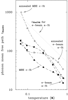 FIG. 4.: Phonon mean free path of
as-deposited and annealed silicon films. As-deposited e-beam a-Si: solid circles; annealed (700∘C, 1 hr)
e-beam a-Si: Open circles; as-deposited MBE Si: solid
squares; annealed MBE Si (500∘C, 1 hr followed by
700∘C, 1.5 hrs): Open squares. The dotted line is
, the TM prediction based on the internal
friction plateau of the as-deposited e-beam a-Si.
Dashed lines are guides for the eye.
ously, these results cannot be used to extract any knowledge
about the annealing of these unknown defects. They do, however,
provide further evidence for the presence of the contaminants
introduced into crystalline silicon during annealing under all
but the most stringent conditions, thus further emphasizing the
need for their identification and control [10].
FIG. 4.: Phonon mean free path of
as-deposited and annealed silicon films. As-deposited e-beam a-Si: solid circles; annealed (700∘C, 1 hr)
e-beam a-Si: Open circles; as-deposited MBE Si: solid
squares; annealed MBE Si (500∘C, 1 hr followed by
700∘C, 1.5 hrs): Open squares. The dotted line is
, the TM prediction based on the internal
friction plateau of the as-deposited e-beam a-Si.
Dashed lines are guides for the eye.
ously, these results cannot be used to extract any knowledge
about the annealing of these unknown defects. They do, however,
provide further evidence for the presence of the contaminants
introduced into crystalline silicon during annealing under all
but the most stringent conditions, thus further emphasizing the
need for their identification and control [10].
Very surprisingly, Fig. 4 shows that the phonon scattering in MBE Si film both before and after annealing is very large as well. Since the contamination that plagued the e-beam a-Si films is not an issue here, secondary ion mass spectroscopy (SIMS) was performed by R. Reedy at the National Renewable Energy Laboratory (NREL) in order to identify other possible chemical impurities. The following chemical elements were detected: boron, cm-3; nitrogen, cm-3; carbon, cm-3; and hydrogen, cm-3. These concentrations were similar in the MBE film and the silicon substrate. Only the oxygen contents differed between substrate ( cm-3) and film ( cm-3). For all these detected impurities, an anneal (500∘C, 1 hr followed by 700∘C, 1.5 hr) caused no measurable change of their concentrations. Since no evidence for such scattering was observed on bare silicon samples from the same batch as used in these experiments[6], the only possible impurity scatterer is the oxygen. But the tenfold increase of oxygen in the MBE film should not lead to a noticeable decrease of the experimental mean free path (defined in the Appendix, Eq. 7), and thus to a decrease of given the relatively small thickness of the film, unless the oxygen in the film somehow acts as a much stronger scattering center. Phonon scattering in oxygen-doped silicon has been found to depend on heat treatment[26, 27] at frequencies in excess of GHz. But, phonons in this frequency range carry heat predominantly above 3 K, and no evidence exists for phonon scattering by oxygen at lower frequencies (corresponds to K).
In an attempt to detect any evidence for structural disorder in this MBE film, an x-ray diffraction (XRD) analysis was performed by M. Sardela and D. Cahill at the University of Illinois (Champaign-Urbana). High resolution open-detector scans around the Si(004) peak showed no difference between measurements conducted on the film side and on the substrate side of the MBE Si film-substrate sample. Full width at half maximum values were found to be almost identical on both sides, and no diffuse scattering or any disorder feature on the film side was seen. In addition, a triple axis reciprocal space map around the Si(004) peak on the film side also could not detect any diffuse distribution nor asymmetry of the Si peak. These observations speak against the existence of grains with different orientations which might cause the phonon scattering.
The near temperature dependence may be suggestive of scattering by sessile dislocations as reported, for example, by Wasserbäch in plastically deformed bulk copper, niobium, and tantalum[28]. If we assume that the coupling between dislocations and phonons is similar, the dislocation density in the MBE film would have to range between and cm-2, which seems rather high for MBE silicon. At this point, no search for dislocations in this MBE film has been undertaken.
MOS-cleaning-and-annealing of the MBE film as described above leads to an increase of shown in Fig. 4, although it remains below the mean free path predicted even for e-beam a-Si, except at the lowest temperature. Thus, noticeable disorder, other than the tunneling states, remains in the MBE Si film even after annealing, although the internal friction of the annealed MBE Si film shown in Fig. 2 give no evidence for any low energy excitations. Thus, the only firm conclusion we can draw at this point is that the defects in the MBE film are not glass-like.
B CaF2 Films
As was just shown, crystalline films produced by crystallizing an
a-Si film or by MBE deposition show little or no evidence
for tunneling states in low temperature internal friction. It is
therefore surprising that a 0.6 m thick film of crystalline
e-beam CaF2 increases the damping of the double paddle
oscillator by more than one order of magnitude, see
Fig. 5. The internal friction of the film itself, as
compared with that of a-SiO2 shown in Fig. 6, is
nearly temperature independent and close to the range found for
all amorphous solids studied to date (with the exception of
certain hydrogenated a-Si films, as discussed in
Ref.[14]). Thus, the large internal friction observed
previously in polycrystalline metal films[1] apparently
also occurs in some crystalline dielectric films. Assuming that
its cause is glass-like excitations, we can again predict an
for the CaF2 film, shown as the dotted
line in Fig. 7. The measured for an
identical CaF2 film, also shown in Fig. 7, is more
than two orders of magnitude smaller than predicted by the TM. We
also measured the phonon mean free path of another crystalline
CaF2 film which was prepared by MBE technique at 750∘C
substrate temperature to improve its structure. However, the
internal friction of the MBE CaF2 film cannot be measured
because of the difficulty of preparing such a film on silicon
paddle oscillators and meeting the requirements of special
cleaning and fabrication at the same time. The of the MBE CaF2 film, though larger than that of
the e-beam one, is still smaller than that predicted by the
TM for the e-beam CaF2 film. Furthermore, it is smaller
than that of an a-SiO2 film prepared by wet-thermal
oxidation, in which the structure is much improved in comparison
with e-beam a-SiO2, and the phonon scattering is
determined solely by the glassy excitations. The
 FIG. 5.: The internal friction of a bare high purity silicon
double-paddle oscillator (solid curve “background”) and of such
a paddle carrying the e-beam CaF2 film on the polished
silicon surface.
FIG. 5.: The internal friction of a bare high purity silicon
double-paddle oscillator (solid curve “background”) and of such
a paddle carrying the e-beam CaF2 film on the polished
silicon surface.
 FIG. 6.: Internal friction of the e-beam CaF2 film
compared to that of bulk a-SiO2 (solid curve). The bulk
a-SiO2 data, measured at 4.5 kHz, is taken from J.E. Van
Cleve, Ph.D. thesis, Cornell, published in Ref.[4]. The
double-headed vertical arrow indicates the range of the
temperature-independent internal friction plateau, measured on a
wide range of bulk amorphous solids as reviewed in Ref.[5].
of the thermal a-SiO2 film
agrees perfectly with that of the TM’s prediction, just as one
would expect for bulk a-SiO2, as shown in
Fig. 7 (see Ref.[6] for details). The of the MBE CaF2 film locates between those of the
thermal a-SiO2 film and a macroscopically as well as
microscopically disordered e-beam a-SiO2 film, in
which the thermal phonon scattering is not dominated by the
tunneling states, also shown in Fig. 7. We suggest that
this MBE CaF2 film, al-
FIG. 6.: Internal friction of the e-beam CaF2 film
compared to that of bulk a-SiO2 (solid curve). The bulk
a-SiO2 data, measured at 4.5 kHz, is taken from J.E. Van
Cleve, Ph.D. thesis, Cornell, published in Ref.[4]. The
double-headed vertical arrow indicates the range of the
temperature-independent internal friction plateau, measured on a
wide range of bulk amorphous solids as reviewed in Ref.[5].
of the thermal a-SiO2 film
agrees perfectly with that of the TM’s prediction, just as one
would expect for bulk a-SiO2, as shown in
Fig. 7 (see Ref.[6] for details). The of the MBE CaF2 film locates between those of the
thermal a-SiO2 film and a macroscopically as well as
microscopically disordered e-beam a-SiO2 film, in
which the thermal phonon scattering is not dominated by the
tunneling states, also shown in Fig. 7. We suggest that
this MBE CaF2 film, al-
 FIG. 7.: Phonon mean free path of two
different CaF2 films. MBE CaF2: solid circles; e-beam
CaF2: solid squares. The dotted lines are the TM prediction
based on internal friction measurements for e-beam CaF2
and for thermal a-SiO2, respectively. Data for the
thermal (open squares) and e-beam (solid stars) a-SiO2 films are taken from Ref.[6]. For thermal a-SiO2, good agreement is shown between
and , which had also been found in
ion-implanted silicon [7], as mentioned in Section I. Dashed
lines are guides for the eye.
though probably more highly ordered than an e-beam one,
contains disorder because the pseudomorphic epitaxial growth is
known to break down at film thickness exceeding
10 nm[29, 30], leading to structural relaxation. Internal
stresses are also expected to result from differential thermal
contraction as the sample is cooled from the deposition
temperature. There is, however, no convincing evidence for
glass-like excitations in this CaF2 film. As in the e-beam a-Si film, some unknown scattering process masks
the effect of the glass-like excitations, if they exist at all.
FIG. 7.: Phonon mean free path of two
different CaF2 films. MBE CaF2: solid circles; e-beam
CaF2: solid squares. The dotted lines are the TM prediction
based on internal friction measurements for e-beam CaF2
and for thermal a-SiO2, respectively. Data for the
thermal (open squares) and e-beam (solid stars) a-SiO2 films are taken from Ref.[6]. For thermal a-SiO2, good agreement is shown between
and , which had also been found in
ion-implanted silicon [7], as mentioned in Section I. Dashed
lines are guides for the eye.
though probably more highly ordered than an e-beam one,
contains disorder because the pseudomorphic epitaxial growth is
known to break down at film thickness exceeding
10 nm[29, 30], leading to structural relaxation. Internal
stresses are also expected to result from differential thermal
contraction as the sample is cooled from the deposition
temperature. There is, however, no convincing evidence for
glass-like excitations in this CaF2 film. As in the e-beam a-Si film, some unknown scattering process masks
the effect of the glass-like excitations, if they exist at all.
C Metal Films
Fig. 8 shows for three e-beam Al films, 0.2, 0.4, and 0.6 m thick. The absence of
any significant dependence on the film thickness validates the
assumption used in our analysis that the scattering occurs
predominantly within the films and not at the interfaces, an
assumption which so far had been based only on the smoothness
observed on the free surfaces as listed in Table II. The dotted
line is the prediction for based on the
internal friction of the e-beam Al film reported
 FIG. 8.: Phonon mean free path for e-beam Al films that are 0.2 m (open triangles), 0.4 m
(open squares), and 0.6 m (open diamonds) thick. The dotted
line is the TM prediction based on internal friction (see Table
III). Dashed lines are guides for the eye.
earlier[1] (see also Table III). As for the two previous
examples, the observed phonon scattering far exceeds the
scattering expected on the basis of the TM.
FIG. 8.: Phonon mean free path for e-beam Al films that are 0.2 m (open triangles), 0.4 m
(open squares), and 0.6 m (open diamonds) thick. The dotted
line is the TM prediction based on internal friction (see Table
III). Dashed lines are guides for the eye.
earlier[1] (see also Table III). As for the two previous
examples, the observed phonon scattering far exceeds the
scattering expected on the basis of the TM.
In Ref.[1], it had been shown that the low temperature
internal friction of an Al film on a Si substrate was very
similar to that of heavily deformed bulk Al. It was therefore
interesting to compare the phonon mean free path in the film
with that observed in deformed bulk Al. For that purpose, a
99.999% pure polycrystalline Al rod (2.5 mm in diameter and
25.7 mm long) was first annealed at 560∘C and subsequently
stretched by 5%. Its thermal conductivity, measured by the
standard steady-state technique, is shown in Fig. 9
along with that of bulk a-SiO2. The steep rise of the
thermal conductivity of the bulk Al above 0.1 K is caused by the
onset of heat transport by normal state electrons. However, below
that temperature, heat is expected to be carried predominantly by
the lattice, and a temperature dependence similar to that of the
bulk glass (a-SiO2) is observed. Although the magnitude
is three times smaller, it still falls within the glassy range in
thermal conductivity, see Fig. 1 in ref. [31].
The phonon thermal conductivity of the 0.2 m e-beam Al
film, as calculated from in
Fig. 8, is also shown in Fig. 9. Above 0.1 K,
the thermal conductivity of the deformed bulk Al and the phonon
thermal conductivity of the e-beam Al film show the
difference between the heat transport by electrons and phonons,
and by the phonons alone, separated here experimentally for the
first time. Below 0.1 K, the phonon thermal conduc-
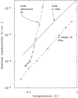 FIG. 9.: The thermal conductivity of 5% deformed bulk Al. The
thermal conductivity of a bulk a-SiO2, taken from
Ref.[32], along with the phonon thermal conductivity of the
0.2 m thick e-beam Al film converted from their phonon
mean free path shown in Fig. 8, is shown for
comparison.
tivity of the e-beam Al film is very close to that of the
deformed bulk sample. This suggests that the defects which
scatter the phonons in the film are very similar to those in the
heavily deformed bulk sample. The same conclusion had been
reached previously in internal friction measurements as stated
above. The defects causing the internal friction had been
tentatively identified as dislocations or dislocation
kinks[1]. It is tempting to suggest that the thermal
phonons in the films are scattered by the same defects. Since we
see in Fig. 8 that and of the e-beam Al films are not connected by the
TM, we can conclude that the same holds for the deformed bulk Al
because of the similarity in the internal friction and phonon
mean free path between the thin films and the bulk samples. Thus,
the non-glasslike phonon scattering phenomena observed in this
work are not limited to thin films alone. In addition, the
defects or the mechanisms causing the resonant scattering of
thermal phonons in heat conduction and those leading to the
relaxational process in internal friction may not even be
related, as shown by the following observation.
FIG. 9.: The thermal conductivity of 5% deformed bulk Al. The
thermal conductivity of a bulk a-SiO2, taken from
Ref.[32], along with the phonon thermal conductivity of the
0.2 m thick e-beam Al film converted from their phonon
mean free path shown in Fig. 8, is shown for
comparison.
tivity of the e-beam Al film is very close to that of the
deformed bulk sample. This suggests that the defects which
scatter the phonons in the film are very similar to those in the
heavily deformed bulk sample. The same conclusion had been
reached previously in internal friction measurements as stated
above. The defects causing the internal friction had been
tentatively identified as dislocations or dislocation
kinks[1]. It is tempting to suggest that the thermal
phonons in the films are scattered by the same defects. Since we
see in Fig. 8 that and of the e-beam Al films are not connected by the
TM, we can conclude that the same holds for the deformed bulk Al
because of the similarity in the internal friction and phonon
mean free path between the thin films and the bulk samples. Thus,
the non-glasslike phonon scattering phenomena observed in this
work are not limited to thin films alone. In addition, the
defects or the mechanisms causing the resonant scattering of
thermal phonons in heat conduction and those leading to the
relaxational process in internal friction may not even be
related, as shown by the following observation.
The alloy Al 5056 in bulk form has an exceptionally small low
temperature internal friction, even as a sputtered film (Table
III), which has been explained by dislocation pinning[1].
The in this film, however, is still close to
that of all other metal films, see Fig. 10. It follows
that pinning of dislocations has no influence on the thermal
 FIG. 10.: Phonon mean free path for a
0.4 m thick e-beam Al film: open squares; for a
0.5 m thick sputtered alloy Al 5056 film: solid circles; for
a 0.1 m thick e-beam Ti film: solid triangles; and for
a 0.1 m thick e-beam Cu film: solid squares. The
thermal conductivity of for the 5% deformed bulk Al is converted
to its mean free path: open circles. The labelled dotted lines are
TM predictions of based on internal
friction measurements (see Table III). The solid curve is the
phonon mean free path in bulk a-SiO2 taken from
Ref.[32]. Dashed lines are guides for the eye.
phonon scattering. We conclude that the mechanisms causing the
internal friction and the thermal phonon scattering are not
understood.
FIG. 10.: Phonon mean free path for a
0.4 m thick e-beam Al film: open squares; for a
0.5 m thick sputtered alloy Al 5056 film: solid circles; for
a 0.1 m thick e-beam Ti film: solid triangles; and for
a 0.1 m thick e-beam Cu film: solid squares. The
thermal conductivity of for the 5% deformed bulk Al is converted
to its mean free path: open circles. The labelled dotted lines are
TM predictions of based on internal
friction measurements (see Table III). The solid curve is the
phonon mean free path in bulk a-SiO2 taken from
Ref.[32]. Dashed lines are guides for the eye.
phonon scattering. We conclude that the mechanisms causing the
internal friction and the thermal phonon scattering are not
understood.
A comparison between and is shown in Fig. 10 for four metal films: Al, alloy Al 5056, Ti, and Cu, with the phonon mean free path of a-SiO2 for comparison. The apparent lack of correlation between and enable us to generalize the same conclusion from the Al films to other metallic films, which is that if glass-like lattice vibrations exist in them, their effect is masked by the unknown defects.
As observed in internal friction[1], is unaffected by superconductivity ( is 0.4 K for Ti, 0.92 for alloy Al 5056[33], and 1.2 K for Al, ). It is concluded that phonon scattering by electrons is unimportant. Klemens has derived an expression for the phonon-electron scattering coefficient in terms of the electron-phonon scattering coefficient [34]. Using the value for measured by Berman and MacDonald for pure copper[35, 36], we calculate (of phonons being scattered by electrons) at 1 K to be m. This phonon scattering rate (due to electrons) is more than an order of magnitude less than the phonon scattering rate observed in Fig. 10 for the Cu film. Note that the calculation of 15 m should not be taken too seriously as its assumptions[37] of the adiabatic principle, of a phonon Debye spectrum, and of a free electron gas may not be adequate at these temperatures for a thin polycrystalline Cu film with a residual resistivity ratio of 2[1]. Nevertheless, this estimate agrees with our observation that electron-phonon interaction is not significant in our experiment.
IV Conclusions
Measurements of the thermal phonon mean free path on films of amorphous and MBE Si, of polycrystalline and MBE CaF2, of pure metallic Al, Cu, and Ti, and of the metallic alloy Al 5056 below 1.0 K have revealed, in all cases, similar strong phonon scattering. Scattering by surface and interface roughness can be excluded, since nearly the same has been observed in Al films of different thicknesses. In searching for the origin of this phonon scattering, we have also measured the low temperature internal friction of the Si and CaF2 films (that of the metal films had been measured previously, Ref.[1]) and also the thermal conductivity of a bulk Al rod after a 5% plastic elongation. In all cases, was found to be much smaller than based on the internal friction and assuming that the lattice vibrations are glass-like. The discrepancy is particularly striking for the MBE Si film in which no internal friction was observed, yet was similar to that found in all other films. In this case, the phonon scattering is particularly puzzling since the film is expected to be structurally more perfect. In all other films, macroscopic defects like grain boundaries, voids, cracks, or dislocations may be the cause for the phonon scattering. In the deformed bulk Al, the phonon mean free path was found to be equal to that in thin Al films. Since in the bulk sample, individual dislocations or aggregates thereof are likely phonon scatterers, they may also be the cause for the scattering in the films. However, dislocation motion, presumably tunneling, which has been invoked to explain the internal friction of deformed Al and of Al films (see Ref.[1, 38]) is an unlikely cause for the thermal phonon scattering since the same in Al was also found in the alloy Al 5056, in which dislocation motion appears to be suppressed, resulting in a greatly reduced internal friction. In conclusion, both internal friction and phonon scattering have been shown to be sensitive probes for thin film disorder, including that in MBE Si. The nature of such disorder and the mechanisms by which it affects the elastic and thermal properties are completely unknown. No evidence for the existence of glass-like lattice vibrations has been detected.
Acknowledgements
We gratefully acknowledge the help of Aaron Judy with the AFM measurements, Glen Wilk in preparing the MBE Si film at Texas Instruments (Dallas), and Ken Krebs in fabricating the MBE CaF2 film at the University of Georgia (Athens) and in providing very useful information on that film’s defects. We thank Mauro Sardela and David Cahill for XRD analysis at the University of Illinois (Champaign-Urbana) and Bob Reedy for the SIMS investigation of the MBE Si film at the National Renewable Energy Laboratory. We also thank R.S. Crandall for fruitful discussions. This work was supported by the National Science Foundation, Grant No. DMR–9701972, the National Renewable Energy Laboratory, Grant No. RAD-8-18668, and the Naval Research Laboratory. Additional support was received from the Cornell Nanofabrication Facility, NSF Grant No. ECS–9319005, and the Cornell Center for Materials Research, Award No. DMR-9121564.
Appendix
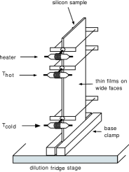
The technique used in this investigation for the measurement of the thermal phonon mean free path in thin films has been described before[6]. Although the experimental schematic resembles that of a thermal conductivity measurement, see Fig. 11, it should be emphasized that our experiment leads directly to a thermal phonon mean free path, rather than to a thermal conductivity , from which the mean free path has to be calculated using the gas-kinetic expression
| (7) |
which requires knowledge of the specific heat of the heat carrying excitations or phonons traveling with an average velocity . In amorphous solids, for example, this cannot be measured. It can only be calculated from through the use of the Debye model.
The analysis of the heat conduction measurements on the silicon substrate carrying the film requires a Monte Carlo simulation which, though straightforward, is nonetheless time-consuming. By strictly adhering to the specifics as listed below (including sample and clamp geometry), one can extract the phonon mean free path in a film, (called in this paper), from (the experimentally measured phonon mean free path of the film-substrate sample) without having to repeat any MC simulations, as will be shown in this Appendix.
Fig. 12 is a plot of the results of MC simulations on a
film-substrate sample with dimensions typically used in this
investigation. For any particular simulation,
is an input parameter where is the film thickness. The
output parameter is , a simulated phonon mean free
path of the film-substrate sample. To determine , one sets an equal to an
in Fig. 12 to find the
![]()
 FIG. 12.: Typical plot of versus where is the film thickness. Normalizing with respect to allows the same plot to be used for
different film thicknesses as long as the sample and clamp
geometry has not changed (see text for details). The actual code
of the Monte Carlo programs may be found in
Ref.[39].
corresponding ; multiplying by then
yields the desired value, , that directly
corresponds to the measured .
FIG. 12.: Typical plot of versus where is the film thickness. Normalizing with respect to allows the same plot to be used for
different film thicknesses as long as the sample and clamp
geometry has not changed (see text for details). The actual code
of the Monte Carlo programs may be found in
Ref.[39].
corresponding ; multiplying by then
yields the desired value, , that directly
corresponds to the measured .
In order to use Fig. 12 as above, the film-substrate sample must be mounted as shown in Fig. 11. Furthermore, the four thin sides of the high purity silicon substrate must be completely roughened (by sandblasting, for example) while the two wide faces must be smooth from Syton polishing, for example), as explained in Ref.[6]. Any film of thickness must cover both wide faces entirely and uniformly. The height of the sample above the top of the base clamp should be 44.5 mm, the width of the sample 7 mm, and the thickness of the substrate 0.279 mm. The height of the heater, cold thermometer, and hot thermometer clamp above the top of the base clamp should be 41 mm, 4 mm, and 25 mm, respectively. The two interfaces between the heater clamp and the sample (areas of contact) should each be of dimensions mm2 while the four interfaces between the thermometer clamps and the sample should each be mm2. The effect of varying these details are discussed in Ref.[6].
REFERENCES
- [1] X. Liu, E. J. Thompson, B. E. White, Jr., and R. O. Pohl, Phys. Rev. B 59, 11767 (1999).
- [2] A. K. Raychaudhuri and R. O. Pohl, Phys. Rev. B 46, 10657 (1992).
- [3] W. A. Phillips, Rep. Prog. Phys. 50, 1657 (1987).
- [4] P. A. Medwick, B. E. White, Jr., and R. O. Pohl, J. Alloys and Compounds 270, 1 (1998).
- [5] K. A. Topp and D. G. Cahill, Z. Phys. B 101, 235 (1996).
- [6] P. D. Vu, J. R. Olson, and R. O. Pohl, J. Low Temp. Phys. 113, 123 (1998).
- [7] X. Liu, P. D. Vu, R. O. Pohl, F. Schiettekatte, and S. Roorda, Phys. Rev. Lett. 81, 3171 (1998).
- [8] W. Kern, RCA Eng. 28, 99 (1983).
- [9] Recipe given by staff at the Cornell Nanofabrication Facility, Ithaca, New York, and dubbed “Piranha-etch”.
- [10] X. Liu, R. O. Pohl, S. Asher, and R. S. Crandall, J. Non-cryst. Solids 227-230, 407 (1998).
- [11] T. Klitsner and R. O. Pohl, Phys. Rev. B 36, 6551 (1987).
- [12] G. S. Kumar, G. Prasad, and R. O. Pohl, J. Mat. Sci. 28, 4261 (1993).
- [13] D. G. Cahill, Rev. Sci. Instrum. 61, 802 (1990).
- [14] X. Liu and R. O. Pohl, Phys. Rev. B 58, 9067 (1998).
- [15] C. L. Spiel and R. O. Pohl, Rev. Sci. Instr. (to be submitted).
- [16] P. W. Anderson, B. I. Halperin, and C. M. Varma, Philos. Mag. 25, 1 (1972).
- [17] W. A. Phillips, J. Low Temp. Phys. 7, 351 (1972).
- [18] J. Jäckle, Z. Phys. B 257, 212 (1972).
- [19] N. W. Ashcroft and N. D. Mermin, Solid State Physics (Saunders College, Philadelphia, 1976), p.458.
- [20] E. T. Swartz and R. O. Pohl, Rev. Mod. Phys. 61, 605 (1989).
- [21] G. L. Olson and J. A. Roth, Mat. Sci. Rep. 3, 1 (1988).
- [22] R. C. Weast, ed., CRC Handbook of Chemistry and Physics 67 (CRC Press, Inc., Boca Raton, Florida, 1986), p.E-43.
- [23] D. Williamson, S. Roorda, M. Chicoine, R. Tabti, P. A. Stolk, S. Acco, and F. W. Saris, Appl. Phys. Lett. 67, 226 (1995).
- [24] J. S. Custer, M. O. Thompson, D. C. Jacobson, J. M. Poate, S. Roorda, W. C. Sinke, and F. Spaepen, Appl. Phys. Lett. 64, 437 (1994).
- [25] S. Roorda, W. C. Sinke, J. M. Poate, D. C. Jacobson, S. Dierker, B. S. Dennis, D. J. Eaglesham, F. Spaepen, and P. Fuoss, Phys. Rev. B 44, 3702 (1991).
- [26] G. Schrag, M. Rebmann, C. Wurster, F. Zeller, K. Lassmann, and W. Eisenmenger, Phys. Stat. Sol. (a) 168, 37 (1998).
- [27] F. Zeller, K. Lassman, and W. Eisenmenger, Physica B 263-264, 108 (1999).
- [28] W. Wasserbäch, Phys. Stat. Sol. 128, 55 (1991).
- [29] N. S. Sokolov, N. L. Yakovlev, and J. Almeida, Solid State Commun. 76, 883 (1990).
- [30] K. Krebs, private communication.
- [31] E. Thompson, P. D. Vu, and R. O. Pohl, Phys. Rev. B (in press).
- [32] R. C. Zeller and R. O. Pohl, Phys. Rev. B 4, 2029 (1971).
- [33] W. Duffy, Jr., J. Appl. Phys. 68, 5601 (1990).
- [34] P. G. Klemens, Encyclopedia of Physics, vol. 14, S. Flügge, ed., (Springer Verlag, Berlin, 1956) p. 198.
- [35] R. Berman and D. K. C. MacDonald, Proc. Roy. Soc. A211, 122 (1952).
- [36] P. Lindenfeld and W. B. Pennebaker, Phys. Rev. 127, 1881 (1962).
- [37] H. von Löhneysen and F. Steglich, Z. Phys. B 29, 89 (1978).
- [38] E. Thompson and R. O. Pohl, Mat. Res. Soc. Symp. Proc. 562 (1999), in press.
- [39] P. D. Vu, Phonon Scattering in Thin Films Below 1 K, Ph.D. thesis, Cornell University (1999).