Evidence for coexistence of the superconducting gap and the pseudo - gap in Bi-2212 from intrinsic tunneling spectroscopy
Abstract
We present intrinsic tunneling spectroscopy measurements on small Bi2Sr2CaCu2O8+x mesas. The tunnel conductance curves show both sharp peaks at the superconducting gap voltage and broad humps representing the -axis pseudo-gap. The superconducting gap vanishes at , while the pseudo-gap exists both above and below . Our observation implies that the superconducting and pseudo-gaps represent different coexisting phenomena.
PACS numbers: 74.25.-q, 74.50.+r, 74.72.Hs, 74.80.Dm
The existence of a pseudo-gap (PG) in the quasiparticle density of states (DOS) in the normal state of high- superconductors (HTSC) has been revealed by different experimental techniques [4, 5, 6, 7, 8, 9, 10, 11]. For a review, see Refs. [11, 12, 13, 14]. Up-to-date, there is no consensus about the origin of the PG, the correlation between the superconducting gap (SG) and PG, or the dependencies of both gaps on material and experimental parameters. A clarification of these issues is certainly important for understanding HTSC.
From surface tunneling experiments, it was concluded that the SG is almost temperature independent [4, 7]. At , it continuously evolves into the PG, which can persist up to room temperature. Furthermore, it was observed that such a superconducting gap has no correlation with and continues to increase in underdoped samples despite a reduction of [4, 5, 7]. This was the basis for a suggestion that the PG-state at is a precursor of superconductivity [12]. On the other hand, surface tunneling into HTSC has several drawbacks[15], e.g. it is sensitive to surface deterioration. The growing controversy requires further studies with alternative techniques.
Intrinsic tunneling spectroscopy has become a powerful tool in studying the quasiparticle DOS inside bulk single crystals of layered HTSC [6, 10, 16, 17, 18, 19] and thus avoiding the sensitivity to surface deterioration. First experiments were recently attempted [6, 17, 18] to study the PG in mesas fabricated on surface of Bi2Sr2CaCu2O8+x (Bi-2212) single crystals. Unfortunately, intrinsic tunneling experiments also have several problems, such as internal heating and stacking faults (defects) in the mesas. To reduce overheating, a pulse technique was applied by Suzuki et al, [6]. The result at was essentially similar to the surface measurements [4], leaving the obscure relationship between SG and PG [6, 17] unresolved.
In this paper we present results of intrinsic tunneling spectroscopy for Bi-2212 mesas with considerably smaller areas, compared to previous studies [6, 17]. Smaller areas allowed us to avoid stacking faults in the mesas and to avoid mixing between the - axis and - plane transport. As a result, clean and clear tunnel-type current-voltage (I-V) characteristics were observed, which allowed us to distinguish superconducting and pseudo - gaps in a wide range of temperatures. In contrast to surface and earlier intrinsic tunneling experiments [4, 6, 17], we have clearly traced different behaviors of the SG and PG. Thorough studies of I-V curves close to revealed that the superconducting gap does vanish, while the PG does not change at . All this speaks in favor of different origins of the two coexisting phenomena and against the precursor-superconductivity scenario of the PG. Finally, we discuss interplay between Coulomb interaction and low dimensionality as a possible mechanism for the c-axis PG in an inherent two-dimensional (2D) system, such as the Bi-2212 single crystals.
Mesas with different dimensions from 2 to 20 m were fabricated simultaneously on top of Bi-2212 single crystals. To reduce the mesa area we adopted a self-alignment technique, see Ref. [19] for details of sample fabrication. The c-axis I-V characteristics were measured in a three-probe configuration. The contact resistance was small, about two orders of magnitude less than the total resistance of the mesa at the corresponding current. All the leads to a mesa were filtered from high-frequency electrical noise. Altogether, more than 50 mesas made on different crystals were investigated. Parameters of the mesas are listed in Table 1. The three figures in the mesa number represent the batch number, the crystal number and the number of the mesa on the crystal, respectively. Letters ”Ar” or ”Ch” indicate whether the mesa was made by Ar-ion or chemical etching. Here we present results for slightly overdoped ( K) and optimally doped ( K) samples. The pristine crystals were slightly overdoped. Overdoped mesas were obtained by wet chemical etching, which does not significantly change the oxygen content. Optimally doped mesas were made by Ar-ion etching, during which mesas partly loose oxygen. Such mesas had larger , -axis resistivity, see Table 1, and pseudo-gap, see Fig. 4.
Our fabrication procedure provides samples with highly reproducible properties. This is illustrated in the
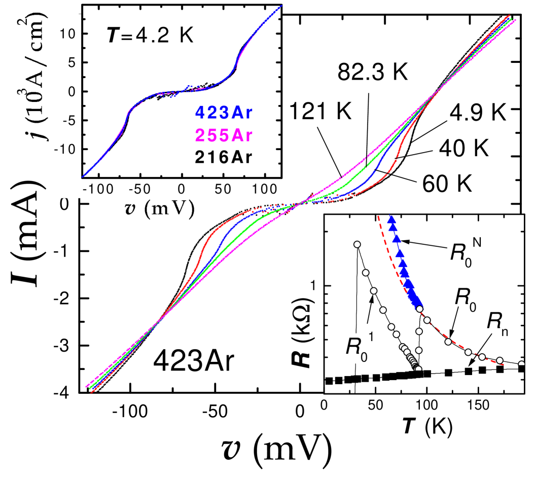
top inset of Fig. 1, in which current density, , vs. voltage per junction, , curves at K are shown for three mesas with different areas from different batches and crystals. Here is the area and is the number of intrinsic Josephson junctions (IJJ’s) in the mesa. We note, that all normalized I-V curves collapse into a single curve. In the following, we will denote quantities corresponding to the whole mesa by capital letters, and those related to an individual IJJ, by small letters. The subscripts ”s”, ”pg” and ”n” will correspond to the superconducting, pseudo-gap and normal state properties, respectively.
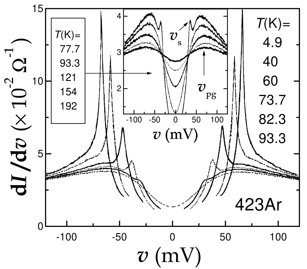
In Fig. 1, curves and in Fig. 2 the voltage dependence of the dynamic conductance are shown for the optimally doped mesa 423Ar at different temperatures. Figs. 1 and 2 exhibit a typical tunnel-junction behavior. At large bias current, there is a well defined normal-state part of tunneling I-V curves with tunnel resistance . decreases by merely 15% from 300 K to 4.2 K and has no feature at , as shown in the bottom inset of Fig. 1. This is in accordance with the pure tunnel junction behavior, for which is expected to be temperature independent. The weak -dependence of indicates an absence of mixing between -axis and -plane transport in our mesas. Previously, however, a strong change of at has been reported for larger mesas [6, 17]. On the other hand, the zero bias resistance, , has a strong temperature dependence, see bottom inset in Fig. 1. Below , is determined by the sub-gap resistance of the first IJJ, , At 40K, a small critical current in the first IJJ appears, see Fig. 3 a), and drops to the contact
resistance. Such a two stage decrease of is due to a deterioration of IJJ’s at the surface of the mesa [20].
At low , there is a sharp peak in , which we attribute to the superconducting gap voltage, . With increasing , the peak at reduces in amplitude and shifts to lower voltages, reflecting the decrease in . At K), the superconducting peak is smeared out completely and only a smooth depletion of (a dip) plus a hump in conductance at mV remain. The dip and the hump are correlated to each other and both flatten simultaneously with increasing , see inset in Fig. 2. Therefore, both reflect the existence of the pseudo-gap in the tunneling DOS. The gradually increases with temperature but the I-V curves remain non-linear nearly up to room temperature. At , the zero-bias resistance, , is fairly well described by the thermal-activation formula,
| (1) |
as shown by the dashed line in bottom inset of Fig. 1.
In agreement with surface tunneling experiments[4, 5], there are no sharp changes at . As shown in bottom inset of Fig. 1, at , evolves continuously into the total (all junctions in the resistive state) sub-gap resistance, . This implies that the PG persists also in the superconducting state. The gradual evolution of the PG hump upon cooling through is most clearly shown in inset of Fig. 2. It is seen that the PG dip/hump feature does not change qualitatively upon cooling through . Moreover, the I-V curve at 77.7 K shows that the superconducting peak at emerges on top of the PG - features which demonstrates a coexistence of both SG and PG features. From Fig. 2 it is seen that by further decreasing the temperature, the superconducting peak
shifts to higher voltages, increases in amplitude and eventually the PG hump is washed out by the much stronger superconducting peak. For optimally doped mesas, the PG hump can be resolved at 60 K, i.e. well below . The gradual opening of at , in addition to the PG, can also be seen from a steeper growth of the total sub-gap resistance, , at , as compared to the thermal-activation behavior of at , as shown in bottom inset in Fig.1.
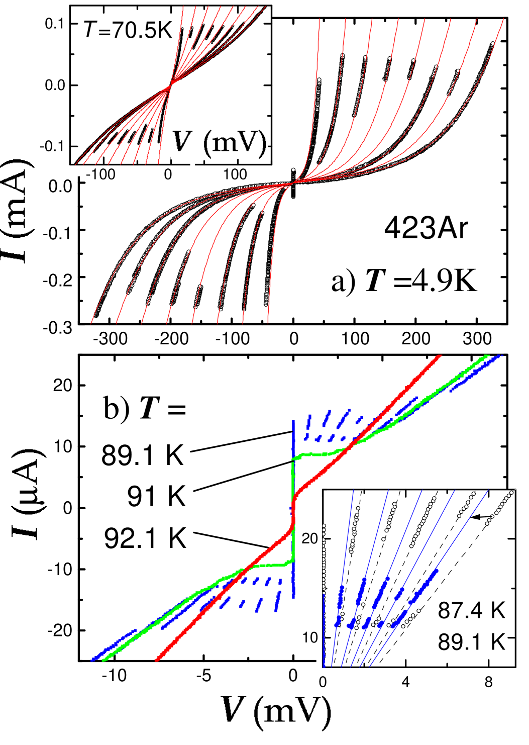
At low bias and , multiple quasiparticle (QP) branches are seen in the I-V curves, representing a one-by-one switching of the IJJ’s into the resistive state [6, 16]. A detailed view of multiple QP branches is shown in Fig. 3 for different . Dots and thin lines in Fig. 3 a) represent the experimental points and a polynomial fit, correspondingly. Only the last branch, having many data-points, was actually fitted, all the other thin lines were obtained by dividing the voltages of this fit, , by the integer number , where is the number of IJJ’s in the resistive state. A good scaling of QP branches is seen, which implies that there is no significant overheating of the mesa at the operational current. If there were overheating, would not go
through the data points because switching of additional IJJ’s would cause a progressive increase of the internal temperature and the branches with increasing count numbers would have lower voltages due to the strong temperature dependence of and .
The separation between QP branches, , is the additional quantity, provided by intrinsic tunneling spectroscopy, which can be used to estimate in a wider range of temperatures. From Fig. 3 b) it is seen that multiple QP branches are clearly distinguishable up to K. From Table 1 it is seen that scales with . The is less than simply because the critical current, , is less than and all IJJ’s switch to the resistive state before they reach the gap voltage, see Fig. 1. The continuously decreases with and vanishes at . In principle, the temperature dependence of is also involved in , since we measure at . However, the inset in Fig.3 b) reveals that still tends to vanish at even if we evaluate at one and the same current for all .
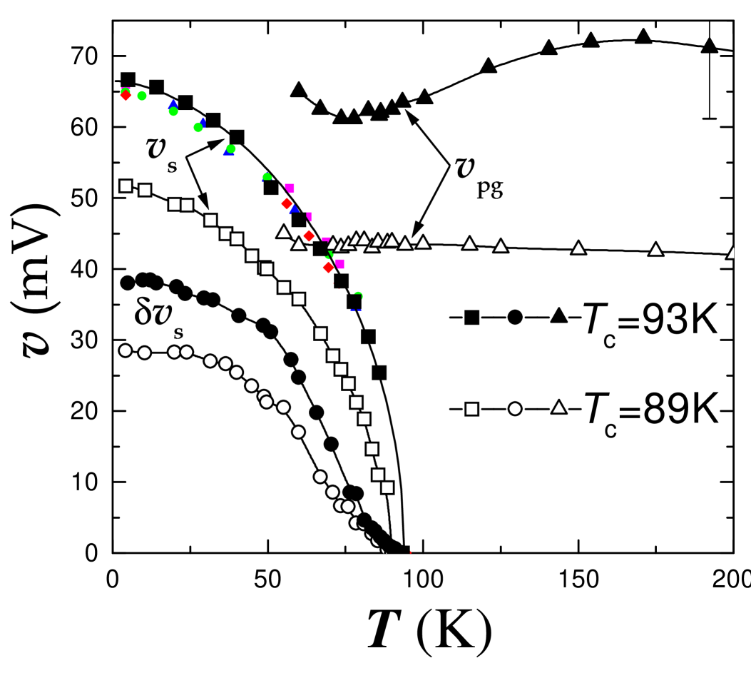
In Fig. 4, the temperature dependencies of the superconducting peaks, (squares), (circles), and pseudo-gap humps, (triangles), are shown for optimally doped (solid) and overdoped (open symbols) samples. Small solid symbols represent for the rest of the mesas listed in Table 1, and the lines are guides for the eye. In agreement with previous studies, both and increase upon going from overdoped to optimally doped samples[4, 5, 7]. The superconducting gap deduced from the sum-gap voltage is meV for the optimally doped sample, and meV for the overdoped one. In contrast to surface tunneling experiments, we observe that decreases considerably with temperature. The robust decrease of from 4.2K to is more than 80 % for the overdoped mesas. Moreover, we can measure in a wider range of and observe that it vanishes at .
All this brings us to the conclusion that the superconducting gap does close at , in agreement with the previous observations of vanishing of the superfluid density (divergence of the magnetic penetration depth) [21] and the Josephson plasma frequency [22]. On the contrary, the PG is almost temperature independent and exists both above and below . Therefore, the SG is not developing from the PG, and these two gaps represent different coexisting phenomena. The recently observed independence of the PG on magnetic field [9] supports our conclusion and also casts doubts about the precursor-superconductivity origin of the PG [12].
One possible ”non-superconducting” PG-scenario is the formation of charge or spin density waves (CDW or SDW) [8, 13]. HTSC’s are composed of quasi-two dimensional electronic systems with a certain degree of Fermi-surface nesting [8], which can make the system unstable with respect to CDW or SDW formation [23, 24]. A CDW or SDW is accompanied by a PG in DOS, detectable by a surface-tunneling spectroscopy [25]. Many similarities exist between the PG in CDW or SDW (including ARPES [24], optical conductivity and NMR [23, 13]) and the PG in HTSC. On the other hand, an opening of the gap due to CDW or SDW is typically accompanied by a metal-insulator transition [23], while the -plane resistivity in Bi-2212 shows the opposite tendency [26].
We would also like to emphasize a similarity between the PG features of -axis tunneling in HTSC and Coulomb PG for tunneling into a two-dimensional electron system (2DES). The Coulomb PG in 2DES is well studied in connection with semiconducting heterostructures [27, 28, 29]. Experimental curves from the inset in Fig. 2 are strikingly similar to ”V-shaped” tunneling characteristics of 2DES [27, 28]. Certainly, the electron system in Bi-2212 is highly two-dimensional. Moreover, a Coulomb origin of the HTSC pseudo-gap would naturally explain the increase of PG with decreasing O-doping and carrier concentration. A large Coulomb PG in low conducting 2DES is due to unscreened long-range Coulomb interaction [28] and/or slow charge accommodation [29]. Large PG could also appear if tunneling occurs via intermediate low conducting BiO layers [14].
An attractive feature of both CDW/SDW and Coulomb PG scenaria is that the PG can persist in the superconducting state. Below , SG and PG are combined into a larger overall gap[13]. This is in agreement with a definite trend for the increase of at , see Fig. 4. This might also help in understanding of large ”superconducting” gaps seen in underdoped HTSC [4, 5]. Whether the CDW/SDW or Coulomb PG scenaria can explain all PG features in HTSC remains to be clarified.
In Conclusion, small mesa structures were used for intrinsic tunneling spectroscopy of Bi-2212. We were able to distinguish and simultaneously observe both superconducting and pseudo gaps in a wide range of temperatures. The superconducting gap has a strong temperature dependence and vanishes at , while the pseudo-gap is almost temperature independent and exists both above and below . This suggests that the pseudo-gap is not directly related to superconductivity.
REFERENCES
- [1] also Institute of Solid State Physics, 142432 Chernogolovka, Russia
- [2] also P.L.Kapitza Institute, 117334 Moscow, Russia
- [3] also IMEGO Institute, Aschebergsgatan 46, S41133, Göteborg, Sweden
- [4] Ch.Renner, et.al, Phys.Rev.Lett. 80 (1998) 149
- [5] N.Miyakawa, et.al, Phys.Rev.Lett. 83 (1999) 1018
- [6] M.Suzuki, et.al, Phys.Rev.Lett. 82(1999) 5361
- [7] M.R.Norman, et.al., Phys.Rev.B 57 (1998) R11093
- [8] N.L.Saini, et.al, Phys.Rev.Lett. 79 (1997) 3467
- [9] K.Gorny, et.al, Phys.Rev.Lett. 82 (1999) 177
- [10] A.Yurgens, et.al., Cond-Mat/9907159
- [11] A.V.Puchkov, et.al, J.Phys.Cond.Mat. 8 (1996) 10049
- [12] M.Randeira, Cond-Mat/9710223
- [13] R.S.Markiewicz, et.al., Cond-mat/9807068
- [14] J.Halbritter, Physica C 302 (1998) 221
- [15] P.Mallet, et.al, Phys.Rev.B 54 (1996) 13324
- [16] K.Schlenga, et.al., Phys.Rev.B 57(1998) 14518
- [17] I.F.G.Parker, et.al., Proc. SPIE 3480(1998) 11
- [18] D.Winkler, et.al, Supercond.Sc.Techn. 12 (1999) 1013
- [19] V.M.Krasnov, et.al, Cond-Mat/0002094
- [20] N.Kim, et.al, Phys.Rev.B 59 (1999) 14639
- [21] S.F.Lee, et.al, Phys.Rev.Lett. 77 (1996) 735
- [22] T.Shibauchi, et.al, Phys.Rev.Lett. 83 (1999) 1010
- [23] G.Grüner, Density Waves in Solids, Addison-Wesley Publishing Company (1994)
- [24] G.H.Gweon, et.al. J. Phys., Cond.Mat. 8 (1996) 9923
- [25] J.J.Kim, I.Ekvall and H.Olin, Phys.Rev.B 54 (1996) 2244
- [26] T.Watanabe, et.al, Phys.Rev.Lett. 79 (1997) 2113
- [27] H.B.Chan, et.al., Phys.Rev.Lett. 79 (1997) 2867; V.T.Dolgopolov, et.al., ibid. 79 (1997) 729
- [28] F.G.Pikus and A.L.Efros, Phys.Rev.B 51 (1995) 16871
- [29] L.S.Levitov and A.V.Shitov, JETP Letters 66 (1997) 215
| mesa | (0) | (0) | (4.2K) | |||
|---|---|---|---|---|---|---|
| (m2) | (K) | (meV) | (mV) | (cm) | ||
| 423Ar | 10 | 93 | 33.3 | 38.5 | 44.9 | |
| 255Ar | 12 | 92.5 | 32.5 | 35.5 | 45.4 | |
| 251Ar | 12 | 92.5 | 32.5 | 35.5 | 44.5 | |
| 211Ar | 12 | 94 | 33.0 | 37 | 44.0 | |
| 216Ar | 10 | 94 | 32.3 | 38.5 | 44.9 | |
| 015Ch | 9 | 89 | 25.8 | 28.5 | 32.3 |