[
The mesoscopic proximity effect probed through superconducting tunneling contacts
Abstract
We investigate the properties of complex mesoscopic superconducting-normal hybrid devices, Andreev-Interferometers in the case, where the current is proped through a superconducting tunneling contact whereas the proximity effect is generated by a transparent SN-interface. We show within the quasiclassical Green’s functions technique, how the fundamental SNIS-element of the such structures can be mapped onto an effective S′IS-junction, where S′ is the proximised material with an effective energy gap . The conductance through such a sample at vanishes if , whereas at the conductance shows a peak at . We propose the Andreev-Interferometer, where can be tuned by an external phase and displays maxima at 0 mod and minima at mod . This leads to peculiar current-phase-relations, which depart from a zero-phase maximum or minimum depending on the bias voltage and can even show intermediate extreme at . We propose an experiment to verify our predictions and show, how our results are consistent with recent, unexplained experimental results.
]
The proximity effect, although already known for many decades (see e.g. [1]), has recently attracted new scientific interest in the context of mesoscopic normal-superconducting hybrid structures, which are now experimentally acessible due to progress in nanofabrication and measurement support technology [2]. Departing from the properties of single junctions [3, 4] and the nonmonotonic diffusion conductance of SN-wires [5, 6, 7], the interest turned to the possibility of tuning the conductance by an external phase [5, 8, 9] or a loop in the normal part [6, 10]. On the other hand, if probed through tunneling contacts [11] the conductance is controlled by the DOS and the induced minigap [12, 13], which can also be controlled by a phase [14] and hence opens another channel for phase controlled conductance of a different sign [15]. If a system contains more than one superconducting terminal, a supercurrent can flow [16, 17], which can be controlled and reversed externally [18]. The situation becomes more difficult and in particular time-dependent, if nonequilibrium is created by applying an external voltage parallel to the junction [19].
This latter situation is substantially simplified, if one of the contacts is separated from the rest of the structure by a tunneling barrier. In that case, the voltage- and phase-drop is concentrated at the barrier and the problem is essentially split into two parts: The time-dependence of the phase at the contact and the proximity effect, which determines the superconducting properties at the normal side of the contact, within the normal metal. In that case, the physics should be basically identical to the case of an S′IS-junction, where the properties of the “superconductor” S′ are entirely controlled by the proximity effect, i.e. we expect a gap of size where, if the junction is long, , the Thouless energy. Hence, we will expect the known [20] physics of such S′IS-contacts: The onset of a tunneling current at at any plus the appearance of a current peak at if . The origin of this peak can be easiest understood within a semiconductor representation of the two superconductors, see e.g.[21].
Such a structure can in principle be manufactured in a controlled manner. To the best of our knowledge, this has not yet been realized in Andreev interferometers. Nevertheless, we are going to discuss the connection to two experiments: Kutchinsky et al. [22] studied the conductance in a T-shaped interferometer with superconducting contacts in a semiconducting systems, where unwanted barriers at the interfaces are likely to occur. Antonov et al. [15] . in turn studied a sample with normal tunneling contacts, which might eventually be connected to superconducting pieces.
Model and basic equations. Mesoscopic proximity systems are efficiently and quantitatively described by the quasiclassical Green’s functions technique, described in [23] and its references 4–6, 49, and 50. In this approach, the microscopic Gor’kov equation is reduced to the more handy Usadel equation by various systematic approximations. At interfaces, this equation is supplemented by boundary conditions ***In our case, deviations from these conditions as discussed in [24] are not likely to occur
| (1) | |||||
| (2) |
These conditions guarantee current conservation. We want to apply them to the case of small transparencies . Here, they enforce that the drop of phase and voltage is concentrated at the insulating layer [12, 25]. The current can thus be expressed as an effective tunneling formula
| (3) | |||||
| (4) |
for the current through the interface. Here, the quasiparticle tunneling current amplitude is
| (6) | |||||
and gives the quasiparticle DOS. This formula is the microscopic formulation of the usual Josephson tunneling formula [26].
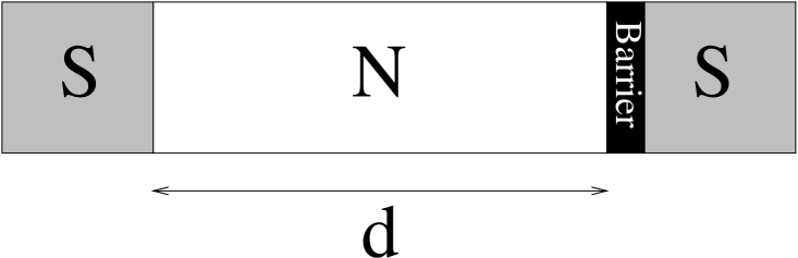
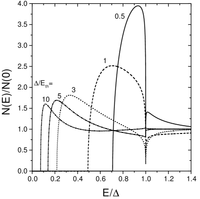
We want to apply this result to the specific case of an SNIS-junction, Fig. 1. Eq. 4 allows to identify this system with an effective IS-Josephson junction, where the “superconductor” is the normal metal layer influenced by the proximity effect. We can characterize by the Green’s functions at the interface calculated from the Usadel equation assuming — in order to be consistent with — a highly resistive interface and consequently a vanishing phase drop over the -part. The “superconductor” S′ has a gap of size , see fig. 2. Thus we expect from a semiconductor model that the system shows a DC supercurrent at and a DC quasiparticle current at . Moreover, at finite temperature, a few empty states below and a few quasiparticles above are available, enabling transport already at (see eq. 6) hence leading to a logarithmic quasiparticle current peak there [27]. Unlike the situation in a massive superconductor, the induced DOS in does not diverge at the gap edge but has a maximum slightly above , see Fig. 2, thus we can conclude that also the peak will be smoothened and be slightly above . Additionally, due to BCS singularity in S, another structure is present in DOS of at , which is weakened with increasing thickness (or decreasing Thouless energy).
Numerical results. In order to obtain quantitative results from eqs. 4,6, the function has to be calculated. It is given by the solution of the Usadel equation
with boundary conditions
at the superconductor and
at the tunneling barrier, through . These nonlinear equations are in general not solvable analytically. Nevertheless, we find from a low-energy expansion that to all orders, which indicates the presence of a gap in the spectrum with a sharp edge (at the convergence radius of the low-energy expansion). At high energies, , the system is decoupled from the boundary conditions at the barrier and
indicating that the deviation from the normal state value is exponentially cut off at those energies. This is consistent with our numerical result, Fig. 2.
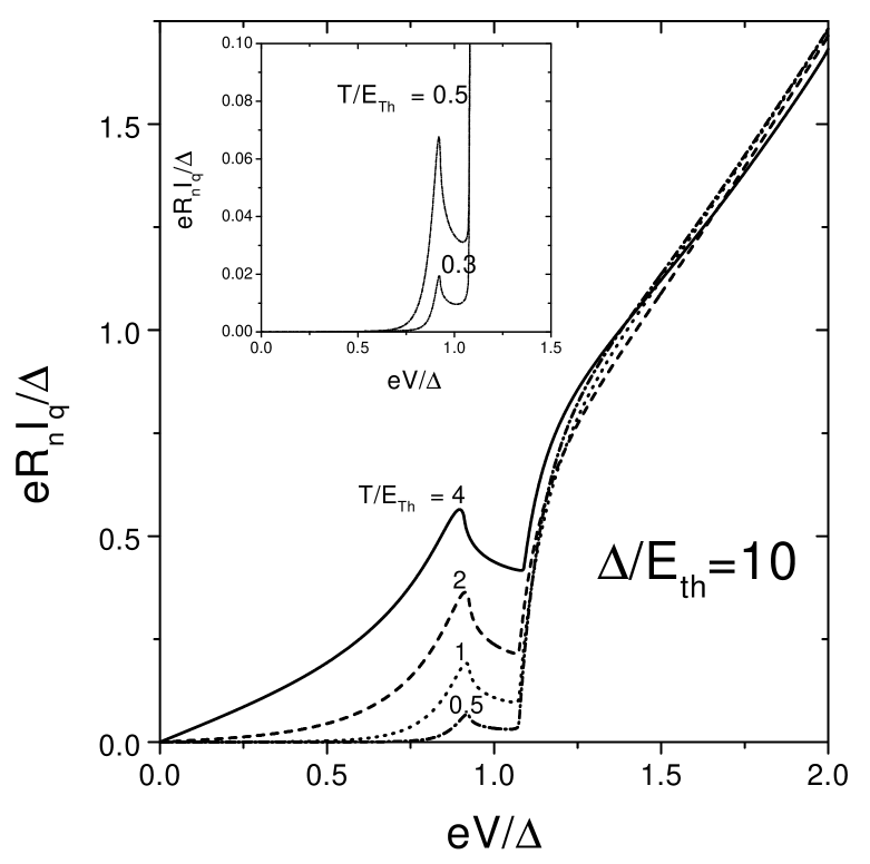
Our qualitative predictions in the preceding section are confirmed by our numerical results, Fig. 3. As predicted, the peaks grow and smear out with increasing temperature, but stay visible up to temperatures far above . Furthermore, the feature becomes more pronounced if is big, i.e. for a shorter junction.
SNIS Andreev interferometers. Even if this type of junction is not prepared on purpose, during the fabrication process an asymmetric barrier can easily show up accidentally, e.g. if the N-metal is a highly doped semiconductor and a Schottky-barrier is likely to occur or if the structure is prepared out of two layers within a two-step shadow evaporation technique [28].
As a particular example, we discuss a specific set of experiments [22].
Unfortunately, the interface resistance has not been systematically investigated there, but a Schottky barrier is likely to occur in this system. As a model, we consider the interferometer Fig. 4 discussed already in [15] in the case when the tunneling barriers are strong and all four reservoirs are superconducting.
The phase difference allows to control the strength of the proximity effect, manifested here in the size of the minigap , which varies between at integer and at half-integer numbers of flux quanta. The influence of the phase difference in the interferometer is hence most pronounced for . The I-V characteristics at a fixed phase, Fig. 4 resembles the form already discussed in Fig. 3 but is slightly smoothened.
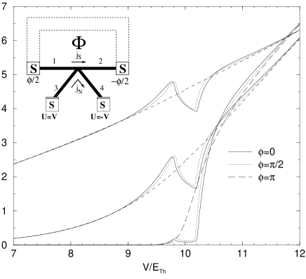
At fixed temperatures and voltages, the I- relation shows many shapes including zero-field minima and maxima as well as additional extrema at intermediate phases as depicted in Fig.5. This can be traced back to the motion of : At , a bigger gap slightly lowers the current (see left upper in fig. 5), at , we are in the vicinity of the induced peak, which only shows up due to , so the current is rather suppressed by shifting the gap (see right upper in fig. 5). At , the situation is more subtle: The current will be maximum, if the edge at , which will be achieved at intermediate . Due to symmetry reasons, this does not only result into a phase shift, but into an intermediate maximum. Comparing and , one finds that depending on the particular voltage, there is a competition of the sharpness of the induced gap at increasing on the current above the gap edge but decreasing it below the gap edge, which have to be traded off and e.g. in Fig. 5, left lower, lead to a higher current at . At , both peaks in the DOS contribute to the current, which is again leads to a zero-phase maximum, right lower.
A similar multitude of structures was observed in the in the interferometer studied in the last section in the experiments by e.g. by Antonov et al., see [15]. In that paper, the conductance of an Andreev-interferometer as probed through normal tunneling contacts was investigated. For technical reasons, small pieces of Aluminum had to be deposited at the site of the barriers, which may become superconducting, rendering the structure a superconducting rather than a normal tunneling contact. As a result, there have been oscillations with intermediate maxima observed under certain bias conditions, which are compatible with our predictions [29].


The oscillation amplitude, see Fig. 6 shows a remarkable peak structure. In the experiments [22], this effect will be washed out due to the 2D-geometry, however, a pronounced splitting of the conductance peak around is observed. Remarkably and in agreement with [22], the oscillation amplitude in 6 only depends weakly on temperature, although we would have expected a strong T-dependence at least of the sub-gap peak. This observation in agreement with the experiments and makes it a likely explanation of the observed peak splitting.

Our predictions can be studied in a more genuine setup like in the inset of Fig. 4, which is also remarkable to another reason: The attached tunneling contacts cool the distribution function in the normal metal by removing quasiparticles[30]. This should also influence the supercurrent between the other two superconducting reservoirs in a way opposite to [31]. Whether or not this also leads to -junction behavior requires more detailed knowledge of the efficiency of the cooling. The experimental detection of the -junction along the lines of [32] require detailed knowledge of the current-phase-relations 3 and 4 (in that terminology the the control line), which is provided by our study.
Summary and Conclusions We have discussed the physics of proximity systems probed through a superconducting tunneling contact. We showed, how these can be understood as junctions between two different superconductors separated by a tunneling barrier. This leads to a peculiar current-voltage characteristic containing a huge step preceded by a small peak at . We discussed the phase-dependence of that current in a typical Andreev-Interferometer and outlined connections to existing and future experiments.
We would like to acknowledge useful discussions with A.D. Zaikin, G. Schön, T.M. Klapwijk, J.J.A. Baselmans, H. Weber, T. Heikkilä, O. Kuhn, and R. Taboryski. This work was supported by the DFG through SFB 195 and GK 284 and by the EU through the EU-TMR “Superconducting Nanocircuits”.
REFERENCES
- [1] P.G. de Gennes, Rev. Mod. Phys. 36, 225 (1964).
- [2] Special issue of Superlattices and Microstructures, 25, 627–1288 (1999) ed. P.F.Bagwell, and references therein.
- [3] G.E. Blonder, M. Tinkham, and T.M. Klapwijk, Phys. Rev. B 25, 4515 (1982).
- [4] A. Kastalsky et al., Phys. Rev. Lett. 67, 3026 (1991).
- [5] Yu.V. Nazarov and T.H. Stoof, Phys. Rev. Lett. 76, 823 (1996).
- [6] A.A. Golubov, F.K. Wilhelm, and A.D. Zaikin, Phys. Rev. B 55, 1123 (1997).
- [7] H. Courtois et al., J Low Temp. Phys. 116, 187 (1999).
- [8] V.T. Petrashov et al., Phys. Rev. Lett. 74, 5268 (1995).
- [9] A. F. Volkov, A. F. N. Allsopp, and C. J. Lambert, J. Phys. Condens. Matter 8, L45 (1996).
- [10] H. Courtois et al., Phys. Rev. Lett. 76, 130 (1996).
- [11] S. Guéron et al., Phys. Rev. Lett. 77, 3025 (1996).
- [12] A.A. Golubov and M.Yu. Kupriyanov, J. Low Temp. Phys. 70, 83 (1988); JETP 69, 805 (1989).
- [13] W. Belzig, C. Bruder, and G. Schön, Phys. Rev. B 54, 9443 (1996).
- [14] F. Zhou et al., J. Low Temp. Phys. 110, 841 (1998).
- [15] V.N. Antonov, H. Takayanagi, F.K. Wilhelm, and A.D. Zaikin, submitted.
- [16] F.K. Wilhelm, A.D. Zaikin, and G. Schön, J. Low Temp. Phys. 106, 305 (1997).
- [17] H. Courtois, Ph. Gandit, and B. Pannetier, Phys. Rev. B 52, 1162 (1995).
- [18] F.K. Wilhelm, G. Schön, and A.D. Zaikin, Phys. Rev. Lett. 81, 1682 (1998); to appear in the proceedings of the Rencontres de Moriond 1999 conference; to appear in Physica B.
- [19] P. Dubos et al., to appear in Physica B.
- [20] K.K. Likharev, Dynamics of Josephson Junctions and Circuits (Gordon and Breach, N.Y., 1986).
- [21] M. Tinkham, Introduction to Superconductivity, 2nd ed., (McGraw Hill, Singapore, 1996).
- [22] J. Kutchinsky et al., Phys. Rev. B 56, R2932 (1997).
- [23] W. Belzig, F.K. Wilhelm, C. Bruder, G. Schön, and A.D. Zaikin, Superlattices and Microstructures 25, 1251 (1999).
- [24] C.J. Lambert, R. Raimondi, V. Sweeney, and A.F. Volkov, Phys. Rev. B 55, 6015 (1997).
- [25] A.A. Golubov et al., Phys. Rev. B 51, 1073 (1995).
- [26] B. Josephson in R.D. Parks, Superconductivity, (Dekker, N.Y., 1969).
- [27] A. Barone, G. Paterno Physics and applications of the Josephson effect (Wiley, N.Y., 1982).
- [28] H. Weber, private communication.
- [29] V.N. Antonov, private communication.
- [30] M.M. Leivo, J.P. Pekola, and D.V. Averin, Appl. Phys. Lett. 68, 1996 (1996).
- [31] A. Morpurgo, B.J. van Wees, and T.M. Klapwijk, Appl. Phys. Lett. 72, 966 (1998).
- [32] J.J.A. Baselmans, A.F. Morpurgo, B.J. van Wees, and T.M. Klapwijk, Nature 3̄ 397, 45 (1999).