Superconducting and Insulating Behavior in One-Dimensional Josephson …
Superconducting and Insulating Behavior in One-Dimensional Josephson Junction Arrays
Abstract
Experiments on one-dimensional small capacitance Josephson Junction arrays are described. The arrays have a junction capacitance that is much larger than the stray capacitance of the electrodes, which we argue is important for observation of Coulomb blockade. The Josephson energy can be tuned in situ and an evolution from Josephson-like to Coulomb blockade behavior is observed. This evolution can be described as a superconducting to insulating, quantum phase transition. In the Coulomb blockade state, hysteretic current-voltage characteristics are described by a dynamic model which is dual to the resistively shunted junction model of classical Josephson junctions.
PACS numbers: 73.40Gk, 74.50+r
1 INTRODUCTION
The Coulomb blockade of Cooper pair tunneling (CBCPT) is a remarkable phenomena, where a normally superconducting tunnel junction becomes insulating, behaving as a capacitor with a critical voltage for current flow. The CBCPT can be observed when the Josephson coupling energy, is the same order of magnitude as the charging energy, , where is the junction capacitance. The temperature must be low, , and most importantly, the junction must experience a high impedance electromagnetic environment. The electrodynamic environment controls the quantum fluctuations of the Josephson phase, and thereby determines whether superconducting (Josephson-like) or insulating (Coulomb blockade) behavior is observed.
When the electrodynamic environment is described by the impedance , quantum fluctuations of the phase become large if , where k is the quantum resistance for Cooper pairs. Large quantum fluctuations of the phase mean that the number difference of Cooper pairs across the junction becomes a sharply defined quantum variable, as for a coherent state. By realizing this high impedance environment with Josephson tunneling, we realize a unique state of charged matter, where many Bosons (Cooper pairs) are condensed into a state with well specified number.
For a single Josephson junction in an arbitrary, linear electrodynamic environment, the effect of quantum fluctuations on Josephson tunneling is well described theoretically for the case [1]. However, when a single Josephson junction is placed in the environment of several other Josephson junctions, the theory is much less clear. Theoretical work on Josephson junctions arrays has primarily concentrated on two-dimensional (2D) arrays. A phase diagram is often calculated which maps out insulating and superconducting regions, depending on the various parameters of the junctions, , , the normal state tunneling resistance , or the quasiparticle tunneling resistance, (for a review, see [2]). The theory can be related to experimental work on granular thin films of superconducting metals (for a review see [3]) and 2D Josephson Junction Arrays fabricated with electron-beam lithography [4, 5]. Finite size effects, and the interplay between the island stray capacitance and the junction capacitance are generally not considered in the theoretical treatment of Josephson junction arrays. However, experiments on 2D arrays show a connection between the array size and the character of the superconductor-insulator (S-I) transition [6]. The Delft group has also studied long, two-dimensional arrays, which approach a 1D parallel array [7], as well as short 1D series arrays [8, 9]
In this work we will examine experimental results on one-dimensional (1D) arrays of small capacitance Josephson junctions. We will describe the evolution from superconducting to insulating behavior in the arrays, which qualitatively is very similar to that observed in granular thin films and 2D Josephson junction arrays. We argue that the ratio of the junction capacitance to the island stray capacitance is an important parameter for the coupling to a dissipative environment, and therefore is crucial for observation of the S-I transition.
1.1 One Dimensional Arrays
Theoretical work on 1D arrays of small capacitance Josephson junctions has analyzed the charge dynamics of 1D arrays in the Coulomb blockade state [10, 11, 12, 13]. Other theoretical analysis has centered on the questions of determining a phase diagram, and for what values of the array parameters an insulating phase (Coulomb blockade) or Superconducting phase (Josephson effect) can be expected [14, 15, 16, 17]. Theoretical analysis of small capacitance 1D arrays usually begins with simplification of the charging energy. In many cases one takes only ”on site” charging, where only the stray capacitance of each electrode to ground, is considered. A better approximation to the experiments is to reduce the capacitance matrix to a bi-diagonal form, where and the junction capacitance, are taken into account. In experiments, typically . In our experiments, we strive for by making the junction capacitance fairly large ( 1 to 3 fF) and the spacing between junctions very small (m) which leads to a smaller .
When the electrostatic screening length extends over several junctions. The potential due to one excess charge decays exponentially with the characteristic length . This potential profile is known as a charge soliton [18] because the profile moves with the tunneling charge. Reducing the full capacitance to only and is valid only when a ground plane is located closer to the array than the junction spacing. One sample (B6-22 series described below) had a ground plane located m from the array, and other samples had no ground plane. Thus the bi-diagonal capacitance matrix is only approximate. In the absence of a ground plane, the potential distribution will decay less steeply than exponential, and go as at large distance. The charge soliton actually spreads out, and a slightly more effective polarization of the array occurs over the same characteristic distance, [19].
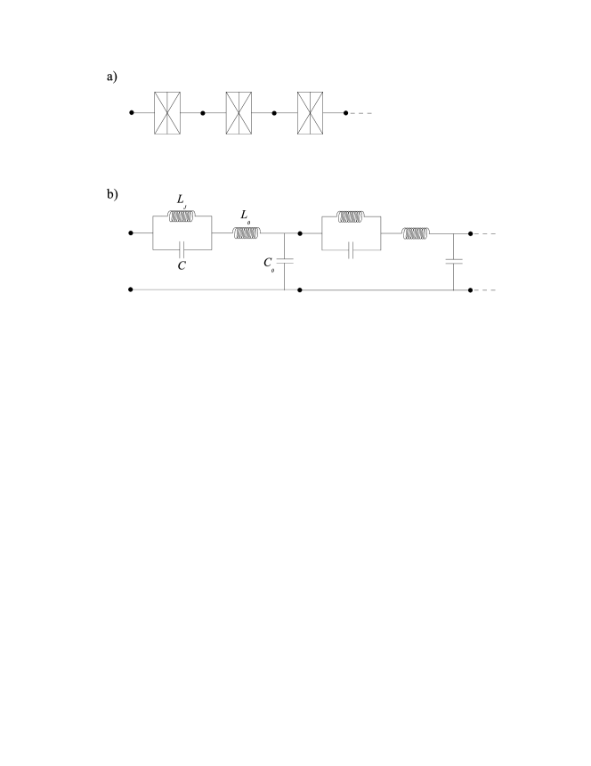
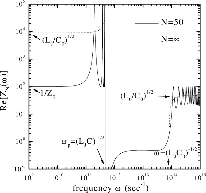
Not only the electrostatics, but also the electrodynamics of the array is effected by a large [20]. For large the junctions become strongly coupled, and the dynamics is dominated by Josephson plasmons. To demonstrate this point we consider an infinite 1D array of Josephson junctions. For small phase gradient, when the current is less than the critical current, , the Josephson phase-current relation can be linearized, and each junction is an effective inductance, , where is the flux quantum. Replacing each Josephson junction by a parallel combination of and , we may calculate the impedance of the 1D network shown in fig 1. The results of such a calculation are shown in fig. 2 for an infinite array, and a finite array with junctions, for typical values of , and in our experiments.
For a finite array, we see a set of discrete resonances which are the Josephson plasmon modes. The width of these resonances is determined by the terminating impedance, . For the infinite array, these resonances form a dense set of modes, where the impedance is much larger than . At frequencies much less than the Josephson plasma frequency, and for the real impedance can be written as,
To observe the CBCPT, it is necessary that and both . If the maximum Cooper pair current (”Zener current” ) is suppressed exponentially and becomes immeasurable, and if the threshold voltage is exponentially suppressed and becomes immeasurable [21]. Thus, requires that . This impedance does not come from electromagnetic fields, as in a usual transmission line, but rather due to long wave-length Josephson plasmons involving the phases of many junctions.
The large ratio in our arrays not only results in a large impedance, and therefore a Coulomb blockade, but also influences the effect of random offset charges. Simulations show that the static background potential due to random offset charge is smoothed by the averaging effects of the large ratio [22]. One would expect that pinning of the charge in some local energy minimum in the array could be practically eliminated. However, simulations show that incoherent charge transport is substantially effected by static random background charge, even in the limit [22, 23, 24, 25]. To our knowledge, the effect of random offset charges on coherent Cooper pair tunneling has not been investigated theoretically.
2 EXPERIMENTAL RESULTS
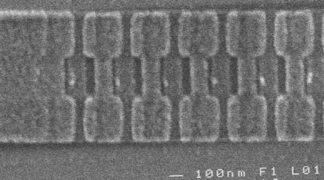
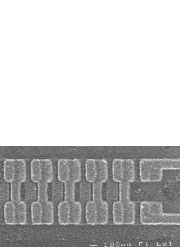
The arrays are actually serially connected SQUIDs (Superconducting Quantum Interference Devices). The SQUID geometry allows one to externally impose a phase shift between neighboring superconducting electrodes by application of a magnetic flux. This external phase shift can be considered as effectively tuning the Josephson coupling energy with an external magnetic field, . Figure 3 shows scanning electron micrographs of two different arrays. The electrodes were Al, deposited on an oxidized Si substrate, with an Al2O3 tunnel barrier. At the right hand side of fig.3 we see how the arrays were terminated. Two different arrangements were used. Figure 3a shows a 2-point termination, where a wide strip connects to the first SQUID. This 2-point arrangement had the disadvantage that expelled magnetic flux from the wide strip focused more flux into the edge loops. Consequently the two edge junctions had a smaller period of modulation with magnetic field. Figure 3b shows the 4-point termination, where no edge effect with the magnetic field was observed. For the 4-point termination, the junctions in the leads are not SQUIDs, and thus do not have a tunable .
Table 1 shows the main parameters of the arrays studied thus far. Samples with the same chip code (B6-##) were made simultaneously on the same chip. The samples are arranged with decreasing . The note indicates whether the array was terminated with a 2 point or 4 point lead configuration. The value of was determined from the measured normal state resistance and the superconducting energy gap, . The charging energy was calculated from the observed area of the junction and the specific capacitance fFm2. Depending on the array parameters, different behavior of the arrays could be observed. We divide these into three different regions discussed below.
| Sample | Note | ||||||
|---|---|---|---|---|---|---|---|
| code | Jun. | (k) | (eV) | (eV) | (k) | ||
| B6-21a | 255 | 1.1 | 586 | 23 | 25 | 8.5 | 2 pt., SI-trans |
| B6-21b | 127 | 1.1 | 586 | 23 | 25 | 8.5 | 2 pt., SI-trans |
| B6-21c | 63 | 1.1 | 586 | 23 | 25 | 8.5 | 2 pt., SI-trans |
| B6-21d | 31 | 1.1 | 586 | 23 | 25 | 8.5 | 2 pt., no CBCPT |
| B6-21e | 15 | 1.1 | 586 | 23 | 25 | 8.5 | 2 pt., no CBCPT |
| B6-21f | 7 | 1.1 | 586 | 23 | 25 | 8.5 | 2 pt., no CBCPT |
| B6-41a | 255 | 1.6 | 406 | 29 | 14 | 10.2 | 4 pt., SI-trans |
| B6-32a | 255 | 2.7 | 227 | 29 | 7.8 | 13.3 | 4 pt. SI-trans at |
| B6-22a | 255 | 4.6 | 142 | 23 | 6.1 | 17.4 | 2 pt., SI-trans |
| B6-22b | 127 | 4.6 | 142 | 23 | 6.1 | 17.4 | 2 pt., SI-trans |
| B6-22c | 63 | 4.6 | 142 | 23 | 6.1 | 17.4 | 2 pt., SI-trans |
| B6-41b | 255 | 4.3 | 149 | 50 | 3.0 | 16.8 | 4 pt., only CBCPT |
| B6-32b | 255 | 8.5 | 78 | 52 | 1.5 | 24 | 4 pt., only CBCPT |
| K9-32 | 255 | 10.4 | 62 | 59 | 1.1 | 26 | 4 pt., only CBCPT |
| K9-43a | 65 | 15.4 | 42 | 59 | 0.71 | 32 | 4 pt., only CBCPT |
| K9-43b | 255 | 15.7 | 41 | 59 | 0.70 | 32 | 4 pt., only CBCPT |
2.1 Superconducting State
For the samples in table 1 with a smaller ratio , the current-voltage (I-V) characteristic exhibited Josephson-like behavior at zero magnetic field. Figure 4 shows the I-V curve of sample B6-21a. Here we see a nearly vertical ”super current” branch of the I-V curve near zero voltage, and a successive set of vertical quasi-particle branches separated in voltage by . The dc load in the bias circuit was such that we could not trace out the negative differential resistance between these vertical quasi-particle branches. At higher voltages the successive quasi-particle branches merge into one flat branch with a current independent of voltage. At even higher voltages, the I-V curve eventually switches to the normal tunneling branch.

The I-V curve shown in fig. 4 is not that expected for arrays of classical, non-interacting Josephson junctions. As the bias is increased in such arrays we would expect an increasing series of switching currents, starting from the lowest critical current in the array. For these small capacitance, strongly coupled Josephson junctions, we rather observe a decrease of the switching current as we move out in voltage, as well as an increase of the retrapping current. We have no quantitative explanation for this observed behavior. We speculate that it has to do with electromagnetic interaction of the junctions, which are strongly coupled due to the very small .
As the magnetic field is increased, the critical current of all junctions is decreased. The slope of the ”critical current” branch also increases, and as is further suppressed, a distinct threshold voltage emerges as the Coulomb blockade of Cooper pair tunneling (CBCPT) becomes observable (see fig. 5)
2.2 Superconductor - Insulator Transition
Figure 5 shows three I-V curves at different magnetic fields. The nearly vertical line (I-V at G) has a finite slope corresponding to about k. The critical current and the hysteretic switching between the ”supercurrent branch” and the quasiparticle branch is off scale for this curve. As the magnetic field is increased the I-V curve develops a very high resistance state for voltages below a threshold voltage, which is the CBCPT. The curve labeled G in fig 5 shows a hysteretic I-V curve in this Coulomb blockade state, meaning that ”back bending” or region of negative differential resistance exists at low current. We will discuss this hysteresis in the next section. The intermediate curve (G)in fig. 5 shows remnants of both types of hysteresis.

Figure 5 shows that the crossover to the CBCPT is characterized by a set of very nonlinear I-V curves. We would like to know the linear response of the array as in undergoes this transition from Josephson-like to Coulomb blockade behavior. To this end we have devised a measurement of the zero-bias resistance, under the condition that the power dissipation by the array is constant. is measured by phase sensitive detection of a small signal excitation with two lock-in amplifiers. The excitation is adjusted so that the product of the two signals Watt.
could be measured versus temperature and magnetic field. Figure 6 displays the results of such measurements. At low magnetic fields (bottom curves of fig. 6), decreases as the array is cooled below the transition temperature of the Al (K) and eventually becomes flat, showing a temperature independent resistive state as . The finite resistance corresponds to the slope of the ”critical current” branch of the I-V curve (see curve in fig. 5). Experiments indicate [26] that in longer arrays the resistance of this ”flat tail” decreases, indicating the non-zero resistance in this ”superconducting” state is due to the finite size of the array. When the magnetic field is increased, the resistance rises and the ”flat tail” remains. Further increasing the magnetic field causes a transition to a different kind of behavior, where increases as , indicating the development of a Coulomb blockade.

We have previously shown [26] how length scaling of could be used to determine the critical point between superconducting and insulating behavior. Length scaling analysis allowed us to determine a critical point where is independent of length. The critical point separates those curves with a ”flat tail” in from those with increasing as . In the experiment shown in fig. 6 we find that this transition occurs at k (see the arrow in fig. 6). The transition does not always occur at , and the measurements displayed in fig. 6 were special in that the array was terminated with a 4 point configuration. The 4 point termination should reduce any series measurement of dissipation arising at the edge of the array. However, one junction is probably not enough to effectively isolate the array from the environment. Further experiments are needed to determine if this transition at is universal.
2.3 Insulating State
When the CBCPT is well developed in the arrays, is essentially infinite, and we have a zero current state below the threshold voltage. Figure 7 shows how the threshold voltage changes with magnetic field on the insulating side of the S-I transition. We typically find that exhibits a sharp cusp as when ( G for this sample). For samples B6-22 and B6-21 where we could measure length effects, we found that was roughly proportional to length. The threshold voltage depends on the magnetic field in a periodic way, with period corresponding the flux quantum in each loop. The magnitude of the current is also periodic in the magnetic field. These observations prove that the current and the threshold voltage are due to Cooper pair tunneling. Although the Cooper pair tunneling is a coherent process, we measure dissipation (finite current and non-zero voltage) because the pair tunneling interacts with dissipative degrees of freedom.
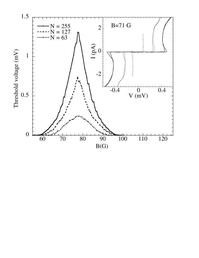
As in the case of a single small capacitance Josephson junction, dissipation arises from excitation of the electromagnetic environment [1] or quasi-particle tunneling [2]. Quasi- particle tunneling becomes important when the voltage drop across any junction exceeds the gap voltage, V. It is important to note that although the voltage over the entire array may be greater than , this voltage is distributed over many junctions. The charge soliton length for Cooper pair charge solitons is determined by an effective capacitance of the junction [12], . The critical voltage goes to zero exponentially for [21]. Hence, at the S-I transition and near this transition the voltage is dropped uniformly over the entire array.
In the insulating state, a very interesting model for charge transport has been developed, which has a direct duality to flux transport in long Josephson junctions [27]. A static version () of this model has been used to explain the magnetic field dependence of the threshold voltage [12]. We have been able to extend the model to the time domain, calculating the dc I-V curve and fitting it to the data. This dynamic model is able to explain the hysteresis observed in the dc IV curve (see fig. 8 and the curve labeled G in fig. 5).
In the insulating state, the Josephson junctions in the 1D chain are described in terms of the dimensionless quasi-charge . If a phenomenological resistance and inductance are introduced together with the capacitance , a sine-Gordon like model can be derived to describe the dynamics of [12]. Soliton solutions exist for this model, and the inductive term is what gives the charge soliton mass, or inertia. We may simplify the full sine-Gordon-like model by dropping the second spatial derivative in order to capture the basics of the dynamic behavior. The array is then viewed as one lumped element, which is valid if the array is shorter than the soliton length, as is the case near the S-I transition. Alternatively, the second time and spatial derivatives may combined by assuming a traveling wave solution to the sine-Gordon-like model. Either approach results in the following equation [28]:
where is the applied voltage, and the dc current is given by the time average . Here saw is a periodic function describing the charging and discharging of the junctions capacitance by single Cooper pair tunneling events. The dot refers to differentiation with respect to dimensionless time, . For the lumped element case, the dimensionless parameter,
determines the amount of hysteresis observed in the dc I-V curve. We have modeled the dissipation arising from Zener transitions in the Bloch energy bands of the single junction Coulomb blockade [21]. To make the model simple we assumed that the resistance is zero below the Zener threshold current, , and characterized by a linear resistance above .
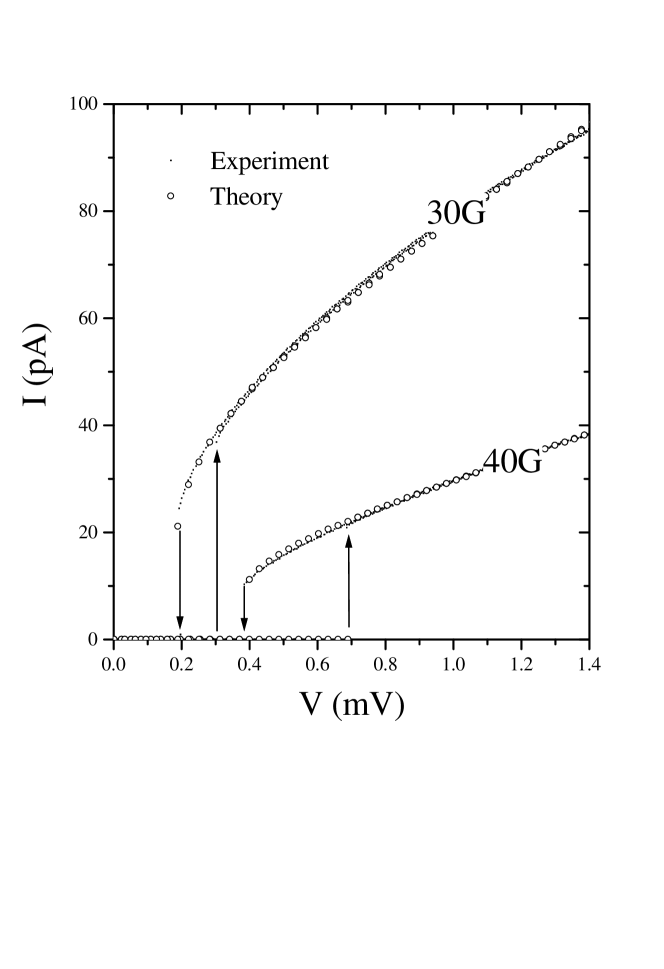
The parameters , , and are fixed for a particular magnetic field (), and are determined from the observed I-V curve. The parameter or is then adjusted to fit the observed amount of hysteresis. Good fits to the data can be made, as seen in fig. 8. However, the inductance required to explain the observed hysteresis is extremely large, H. It is certainly not due to electromagnetic inductance ( H) and too small to be due to Josephson inductance ( H). We do observe that the value of obtained from these fits does diverge as as expected for the Josephson inductance [28].
Although the origin of this large inductance is not understood, we emphasize that an inductive term is absolutely necessary if we are to explain the hysteresis with any dynamic model. We further stress that this hysteresis is clearly associated with the presence of Josephson Coupling in the arrays. Such hysteresis has not been observed in any normal tunnel junction arrays to the best of our knowledge. In our arrays, the normal state behavior shows no clear zero current state. The normal sate is achieved at large magnetic fields (G) where the superconducting energy gap is suppressed. Only a weak remnant of the Coulomb blockade exists in the normal state because the normal tunnel junction resistance is the order of the quantum resistance.
3 CONCLUSION
We have given an overview of the measured transport characteristics of 1D small capacitance Josephson junction arrays. The interplay between Josephson and Charging energies is clearly seen as a transition between Josephson-like to Coulomb blockade I-V curves. Coulomb blockade is observed even when , depending on the length of the array. We point to the importance of the stray capacitance and the long wavelength Josephson plasmons in determining the coupling to dissipation. A quantum phase transition can be observed by measuring the temperature dependence of the zero bias resistance as the effective Josephson coupling is modulated in the arrays. In the insulating state, the hysteretic current voltage characteristics can be explained by a dynamic model which is dual to the usual RSJ model for Josephson junctions.
ACKNOWLEDGMENTS
We wish to acknowledge support from the Swedish NFR, and the EU grant 22953 CHARGE and the EU grant SMT4-CT96-2049 SETamp. Samples were made at the Swedish Nanometer Laboratory.
References
- [1] G.-L. Ingold and Y. V. Nazarov, in Single Charge Tunneling. Coulomb Blockade Phenomena in Nanostructures, Vol. 294 of NATO ASI Series, edited by H. Grabert and M. H. Devoret (Plenum Press, New York, 1992), Chap. 2, pp. 21–107, iSBN 0-306-44229-9.
- [2] G. Schön and A. D. Zaikin, Physics Reports 198, 237 (1990).
- [3] S. Katsumoto, Jour. Low Temp. Phys. 98, 287 (95).
- [4] C. D. Chen et al., Phys. Rev. B 51, 15645 (1995).
- [5] H. S. J. van der Zant et al., Phys. Rev. Lett. 69, 2971 (1992).
- [6] C. D. Chen, P. Delsing, D. B. Haviland, and T. Claeson, Physica Scripta 85, 182 (1991).
- [7] A. van Oudenaarden, B. van Leeuwen, M. P. M. Robbens, and J. E. Mooij, Physical Review B 57, 11684 (1998).
- [8] L. J. Geerligs, V. F. Anderegg, J. Romijn, and J. E. Mooij, Phys. Rev. Lett. 65, 377 (1990).
- [9] A. van Oudenaarden, Ph.D. thesis, Delft University of Technology, 1997.
- [10] A. A. Odintsov, Phys. Rev. B 54, 1228 (1996).
- [11] Z. Hermon, E. Ben-Jacob, and G. Schön, Phys. Rev. B 51, 1234 (1996).
- [12] D. B. Haviland and P. Delsing, Phys. Rev. B Rapid 54, 6857 (1996).
- [13] J. P. Pekola et al., Phys. Rev. B 60, 9931 (1999).
- [14] R. M. Bradley and S. Doniach, Phys. Rev. B 30, 1138 (1984).
- [15] M. C. Cha et al., Phys. Rev. B 44, 6883 (1991).
- [16] S. L. Sondhi, S. M. Girvin, J. P. Carini, and D. Shahar, Rev. Mod. Phys. 69, 315 (1996).
- [17] L. I. Glazman and A. I. Larkin, Phys. Rev. Lett. 79, 3736 (1997), cond-mat/9705169.
- [18] K. K. Likharev, N. S. Bakhvalov, G. S. Kazacha, and S. I. Serdyukova, IEEE Trans. Magnetics 25, 1436 (1989).
- [19] K. K. Likharev and K. A. Matsuoka, Appl. Phys. Lett. 67, 3037 (1995).
- [20] P. A. Bobbert, R. Fazio, G. Schön, and A. D. Zaikin, Phys. Rev. B. 45, 2294 (1992).
- [21] K. K. Likharev and A. B. Zorin, J. Low Temp. Phys. 59, 347 (1985).
- [22] J. Johansson, unpublished .
- [23] A. A. Middleton and N. S. Windgreen, Phys. Rev. Lett. 71, 3198 (1993).
- [24] K. A. Mutsuoka and K. K. Likharev, Phys Rev. B. 57, 15613 (1998).
- [25] J. A. Melsen, U. Hanke, H. O. Mü, and K. A. Chao, Phys Rev. B 55, 10638 (97).
- [26] E. Chow, P. Delsing, and D. B. Haviland, Phys. Rev. Lett 81, 204 (1998).
- [27] E. Ben-Jacob, K. Mullen, and M. Amman, Phys. Lett. A 135, 390 (1989).
- [28] P. Agren, K. Andersson, and D. B. Haviland, Physica B LT 22 proceedings, (1999).