Abstract
Near-field microwave microscopy has created the opportunity for a new class of electrodynamics experiments of materials. Freed from the constraints of traditional microwave optics, experiments can be carried out at high spatial resolution over a broad frequency range. In addition, the measurements can be done quantitatively so that images of microwave materials properties can be created. We review the five major types of near-field microwave microscopes and discuss our own form of microscopy in detail. Quantitative images of microwave sheet resistance, dielectric constant, and dielectric tunability are presented and discussed. Future prospects for near-field measurements of microwave electrodynamic properties are also presented.
1 Introduction
Measurement of the electromagnetic response of materials at microwave frequencies is important for both fundamental and practical reasons. The complex conductivity of metals and superconductors gives insights into the physics of the quasiparticle excitations and collective charge properties of the material. Interesting collective behavior which can be investigated through the complex conductivity includes superconductivity, spin and charge density waves, Josephson plasmons, etc. The dielectric properties of materials give insights into the polarization dynamics of insulators and ferroelectrics. A class of interesting insulating materials, the parent compounds of cuprate superconductors, combine both dielectric and antiferromagnetic behavior because of strong correlations between the charge carriers. Ferromagnetic materials interact with microwaves in several unusual ways, including ferromagnetic resonance and anti-resonance, and spin-wave resonance. In addition, a series of discoveries over the past several decades have found many materials which display coexistence of superconductivity with either antiferromagnetism, or modified forms of ferromagnetism. This wide range of interesting electromagnetic behavior of contemporary materials requires that experimentalists working in this field master many diverse measurement techniques and have a broad understanding of condensed matter physics.
On the practical side, electromagnetic measurements are essential for creating new device technologies and optimizing existing devices and processes. For example, nonlinearities in superconducting materials limit their applications at microwave frequencies to relatively low power uses. Although intrinsic nonlinearities of superconductors will eventually limit their utility, most practical nonlinearities are caused by extrinsic defects in the material or device. Careful characterization of these materials on the length scale of the extrinsic inhomogeneities is required to tackle this problem. Another practical issue is the optimization of materials for frequency-agile applications. Here the issue is measurement of dielectric or magnetic properties which can be tuned with an electric or magnetic field, often in thin-film materials. Yet another important application of electromagnetic measurements is in diagnostic measurements. For example, in a semiconductor integrated circuit process, one needs to measure and control quantities such as sheet resistance, doping profiles, and electromigration in wires. As the speed of microprocessors continues to climb, the microwave properties of materials become increasingly important. Finally, if high-speed integrated circuits fail, it is important to locate the fault (often an open or short) as accurately as possible, and to correct the problem quickly to maintain a high yield. Electromagnetic measurements are thus an important foundation for many emerging technologies.
In this paper we present a new paradigm for electromagnetic measurements of materials. We first briefly review the traditional methods of microwave measurements and point out some of their important limitations. We then present an alternative approach to these measurements through quantitative near-field microwave microscopy. The remainder of the paper is devoted to reviewing the progress we have made in this exciting new field of research.
2 Traditional Microwave Measurements of Electromagnetic Properties
The fundamental electrodynamic quantities of greatest interest are the surface impedance Zs, the conductivity , the dielectric permittivity , and the magnetic permeability . A review of the definitions of conductivity and surface impedance of normal metals and superconductors is given elsewhere in this book. All of these quantities are complex and in general are a function of many variables, including frequency, temperature, magnetic field, electric field, etc.
Traditional microwave measurements of these quantities are typically done on length scales of the free-space wavelength of the signal, which is about 3 cm at 10 GHz. The earliest microwave measurements on superconductors by Pippard were done with the sample acting as a quarter-wavelength resonator [1]. In this case the electromagnetic properties measured are actually an average of the properties along the sample, weighted by the form of the standing-wave resonance pattern. In the case of elemental Pb or Sn this is not much of an issue, but in the case of complicated multi-element oxides it can give rise to misleading results.
A refinement of this technique came through the use of cavity perturbation methods. In this case the sample is immersed in a larger electromagnetic cavity in a region of uniform electric or magnetic field [2, 3]. The properties of the sample can be deduced by comparing the resonant frequency shift and quality factor change from a well-characterized initial (unperturbed) state of the cavity. In this case one measures an average of the electromagnetic properties of the sample, again weighted by the distribution of fields and currents created in the sample [3]. These field and current distributions can be quite complicated for most practical samples [4, 5], becoming simple only for carefully shaped ellipsoids of revolution.
Other resonant techniques have been developed in recent years, particularly for examination of thin-film superconducting materials. These include the parallel-plate resonator technique, in which two congruent films form a transmission line resonator with a length scale on the order of the microwave wavelength [6, 7]. Dielectric resonators are also sensitive to thin-film surface impedance but are averaged over an area on the order of the wavelength [8, 9]. Far-field surface-impedance microscopy techniques use a diffraction-limited beam in a confocal geometry to locally measure the surface impedance at millimeter-wave frequencies, but have a spatial resolution limited to a few millimeters [10, 11].
Non-resonant methods can also be employed to measure electrodynamic properties. For instance, waveguide transmission through thin films has been successful at determining the absolute value of the penetration depth, but provides an average of the properties over the film, again on the length scale of the microwave wavelength.
2.1 Limitations of Traditional Techniques
Although traditional electrodynamics measurement techniques have been very successful, they do suffer from some fundamental limitations. First, they tend to measure a weighted average over large areas of the sample, on the scale of millimeters to centimeters. In the case of oxide thin films, it is often difficult to prepare a material which is homogeneous on such long length scales. For oxide single crystals, doping inhomogeneities have been shown to exist on many length scales from the nanometer to the millimeter range [13]. In addition, surface morphology and second phases (such as flux particles) complicate the response of the crystal to electromagnetic radiation. Hence, traditional electrodynamics measurements yield only an average or overall picture of the sample properties. This means that the intrinsic behavior of the material can be masked by the response of a relatively small fraction of extrinsic or second-phase material. When new materials are measured, there is often a lingering doubt whether the response is due to new intrinsic physics or some unforeseen extrinsic effect.
A second limitation of traditional techniques is the generation of large screening currents, especially near edges, and in the case of superconductors, the subsequent admission of rf magnetic flux into the sample. The rf flux will significantly increase the surface impedance and can easily dominate the response of the material. Such issues have arisen many times in the exploration of electromagnetic properties of new superconducting materials. For instance, early measurements of the penetration depth in thin films of YBCO were corrupted by vortex entry into the films [14]; harmonic generation in superconducting crystals can be dominated by edge effects [15]; and the nonlinear Meissner effect in superconductors can be swamped easily by vortex entry problems [16, 17].
2.2 A new paradigm for electrodynamics measurements
To overcome the limitations of traditional electrodynamics measurements, we have developed a new family of near-field microwave microscopes which permit local quantitative measurements of surface impedance and conductivity, as well as dielectric and magnetic properties. Near-field techniques also relieve us from the “light-cone constraint”, in which the length scales that we can probe with electromagnetic radiation are dictated by the frequency. For instance, this permits broadband electrodynamics measurements to be performed on very fine length scales. Because the spatial resolution is determined by geometrical features which we can control, a class of altogether new electromagnetic experiments can be performed. For example, we now can measure the local tunability of high-frequency electrical properties and make new connections between microstructure and its associated physical properties.
3 An Overview of Microwave Microscopy Techniques
Near-field microwave microscopy is an art which has formed gradually over the years from many different sources. In principle the intellectual founder of the near-field microscopy effort was Synge in his prescient paper of 1928 [18]. However, most practitioners of the art are not familiar with this seminal work despite its importance. Many near-field techniques were developed empirically, some, in fact, developed to solve practical problems in manufacturing. The earliest effort to perform high resolution quantitative microwave measurements seems to be from the ferromagnetic resonance community, led by the work of Frait [19], and later Soohoo [20]. However, not all subsequent developments can be traced back to these roots.
To codify the great variety of work on near-field microwave microscopy of materials, we present a simple picture of the five basic types of microwave microscopy in Fig. 1. Although these classifications are somewhat gross, they allow us to cleanly distinguish the main efforts in the field.
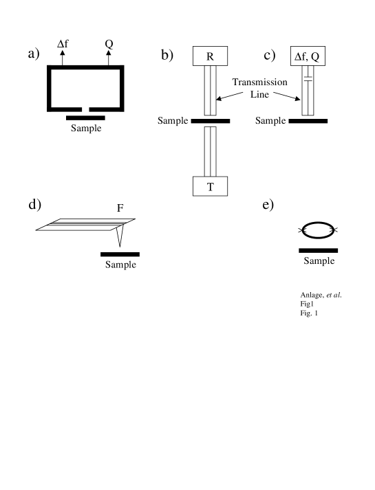
Fig. 1(a) illustrates a traditional microwave cavity resonator with a small hole in one wall. The sample is placed in close proximity to the wall; a small region of the sample, defined by the hole diameter, perturbs the resonant frequency (causing a frequency shift f) and quality factor (Q) of the resonator. Because the hole is so small (0.5 mm diameter for Frait [19]) and the sample makes such a small perturbation to the cavity, one must examine a highly lossy property of the sample, such as ferromagnetic resonance. Ferromagnetic resonance (FMR) gives information about the local internal fields and magnetization of the sample. Frait [19], Soohoo [20] and Bhagat [21] have successfully used this microscope for FMR imaging, while Ikeya [22] has used it for electron spin resonance imaging.
An important variation on this theme was developed by Ash and Nichols [23]. They used an open hemispherical resonator with a flat-plate reflector. The plate had a small hole in it and the sample was positioned close to this hole, but outside the resonator. They did not study FMR, so in order to recover a perturbation signal from the resonator, the sample separation from the hole was modulated at a fixed frequency. They were able to phase-sensitively recover the reflected signal from the resonator to construct a qualitative image of the sample as it was scanned under the hole. These cavity methods all make use of an evanescent mode to couple the resonant cavity to a local part of the sample. In that sense these methods resemble the tapered optical fiber with aperture method of near-field scanning optical microscopy (NSOM) [24, 25].
Fig. 1(b) illustrates a class of non-resonant microscopes in which the sample is placed on or near the end of a microwave transmission line. The complex reflectivity R or transmission coefficient T is measured, and properties of the sample are deduced. The most common technique is to measure reflectivity from a coaxial transmission line terminated (possibly with an air gap) by the sample [26, 27, 28, 29, 30, 31, 32, 33]. Variations include the use of waveguides [34, 35], waveguides covered by a resonant slit [36, 37] and microstrip lines [38] in reflection. Transmission measurements also have been done in the coaxial [31, 39] and waveguide [37] geometries. These techniques have mainly been used to map metallic conductivity or sheet resistance, and dielectric constant. In some cases the measurements are done quantitatively.
Fig. 1(c) shows schematically one of the most sensitive forms of near-field microwave microscopy. The idea is that the sample is put near the open end of a transmission-line resonator, and changes in the resonant frequency and quality factor are monitored as the sample is scanned. This class of techniques differs from that shown in Fig. 1(a) through the use of a “field enhancing” feature at the end of the transmission line, rather than an evanescent aperture in the resonator. The field-enhancing feature sets the scale for the spatial resolution of this class of microscopes. The first embodiment of this concept was conceived for measuring the moisture content of paper [40]. Other embodiments use coaxial transmission lines with the sample in contact with the open end [41, 42, 43, 44, 45, 46, 47, 48, 49, 50, 51, 52, 53, 54, 55, 56], or with an air gap between the probe and the sample [43, 44, 45, 46, 47, 48, 49, 50, 51, 52, 53, 54, 55]. A related far-field technique has been used to image surface resistance and nonlinearity with a scanned dielectric resonator in contact with the sample [8].
The resonant transmission-line technique has proven to be the most quantitative of all the near-field microwave microscopy methods. Quantitative imaging of topography, sheet resistance, dielectric constant and loss, and other quantities has been achieved. In addition, the use of field enhancing features has pushed the spatial resolution of resonant and non-resonant microscopes to the sub-m domain while maintaining the quantitative nature of the measurements.
The last two classes of near-field microscopy techniques are less developed, but show great promise for the future. Fig. 1(d) shows a cantilever with a sharp tip positioned over the sample. This geometry can be used to perform atomic force microscopy to determine the topography of the sample, in addition to microwave microscopy. There are three sub-classes of scanning probe measurements of materials properties at microwave frequencies. The first is to perform localized electron-spin resonance measurements [57]. The tip is used for STM, and a magnetic field is applied to the sample. It is found that a local signal at the Larmor precession frequency can be extracted from the tip and converted into an image of ESR response of the sample. A second embodiment is to create a magnetic field gradient on the sample (e.g., with a small magnetic particle on the tip) while immersing it in an rf magnetic field. The sample will locally satisfy the magnetic resonance condition and exert a force on the cantilever [58, 59]. A third scanning probe method is to simply use a sharp metallized tip to perform “apertureless” near-field microscopy. The sharp tip in close proximity to a metallic sample will locally enhance radiation introduced by a focused far-field beam. If an additional phenomenon can take place in this localized region due to the enhanced field strength, and it can be detected, one has a local microscopic probe of the physics associated with that phenomenon. One important example of this kind of microscopy is apertureless infrared microscopy, where the reflected signal from the region of the probe tip is measured while the tip is periodically dithered up and down [60].
Fig. 1(e) shows the scanning superconducting quantum interference device (SQUID) method of microwave microscopy. The SQUID will generate circulating rf currents when a dc bias is placed across the loop. The frequency of these currents is directly proportional to the applied bias voltage. The currents generate rf magnetic fields which then impinge on the sample. The sample will generate its own response currents which in turn modify the inductance of the SQUID loop. By monitoring the magnetic-field feedback signal required to keep the SQUID in a constant flux state, one can map the electromagnetic response of the sample [61]. This method has the advantage of being very broadband (in principle from rf up to the gap frequency of the superconductor used to make the SQUID, 100 GHz or more) and quantitative.
3.1 Detailed Description of the Maryland Microscope
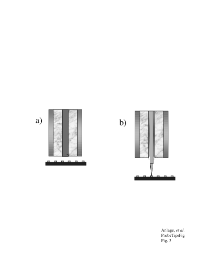
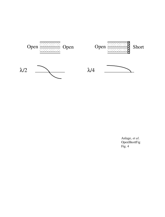
Our group has developed a novel form of near-field scanning microwave microscopy based on the scanned resonator technique (Fig. 1(c)). As shown in Fig. 2, our microscope consists of a resonant coaxial cable which is weakly coupled to a microwave generator on one end through a decoupling capacitor Cd, and coupled to a sample through an open-ended coaxial probe on the other end. In the absence of a sample, the microscope is a half-wave resonator (Fig. 4). As a metallic sample approaches the open end of the coaxial probe, the boundary condition there goes progressively from open circuit to short circuit (e.g., for the blunt probe shown in Fig. 3(a)). In the limit of the sample touching the coaxial probe, the microscope becomes a quarter-wave resonator (Fig. 4). In the process, the resonant frequency shifts by one half the spacing between neighboring modes, which is on the order of 100 MHz. Hence the microscope frequency shift is very sensitive to the probe/sample separation, as well as the electrical properties of the sample (i.e., the conductivity, dielectric constant and magnetic permeability).
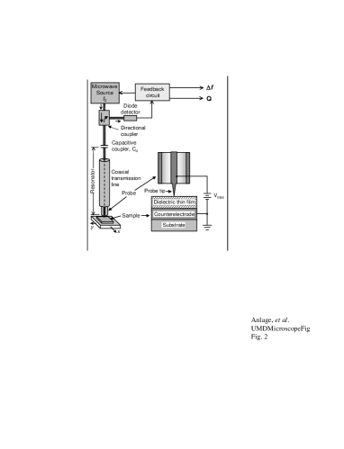
Consider again the limit of the sample very far from the probe. In this case the quality factor of the resonator, Q, is high since only internal dissipation processes (and radiation losses) are active. As the sample approaches the open end of the coaxial probe it must be considered part of the resonant circuit. As such, it will add losses to the system and in general reduce the Q of the microscope. The Q thus gives insight into the additional loss mechanisms introduced by the sample.
As the sample is scanned beneath the probe, the probe-sample separation will vary (depending upon the topography of the sample), causing the capacitive coupling to the sample, Cx, to vary. This has the result of changing the resonant frequency of the coaxial-cable resonator. Also, as the local electrical properties of the sample vary, so will the resonant frequency and quality factor, Q, of the resonant cable. The goal then is to turn the measured quantities f and Q versus position over the sample into quantitative images of sample electrical properties.
A circuit is used to force the microwave generator to follow a single resonant mode of the cable, and a second circuit is used to measure the Q of the circuit, both in real time (Fig. 2) [46, 47]. The microwave source is frequency modulated by an external oscillator at a rate 3 kHz. The electric field at the probe tip is perturbed by the region of the sample beneath the probe’s center conductor. We monitor these perturbations using a diode detector which produces a voltage signal proportional to the power reflected from the resonator. A feedback circuit [47] (Fig. 2) keeps the microwave source locked to a resonant frequency of the transmission line, and has a voltage output which is proportional to shifts in the resonant frequency due to the sample. Hence, as the sample is scanned below the open-ended coaxial probe, the frequency shift and Q signals are collected by a computer. The circuit runs quickly enough to accurately record at scan speeds of up to 25 mm/sec.
To determine the quality factor Q of the resonant circuit, a lock-in amplifier, referenced at , gives an output voltage which is related to the curvature of the reflected power vs. frequency curve on resonance, and hence to Q. To relate and Q, we perform a separate experiment, in which we vary Q using a microwave absorber at various heights below the probe tip, and measure the absolute reflection coefficient of the resonator. If is the reflection coefficient at a resonant frequency , then the coupling coefficient between the source and the resonator is The loaded quality factor of the resonator [62, 63] is QL , where is the difference in frequency between the two points where . The unloaded quality factor, which is the Q of the resonator without coupling to the microwave source and detector, is then Q Q. We also measure , and find that there is a unique functional relationship between Q0 and ; thus, we need to calibrate this relationship only once for a given microscope resonance. In a typical scan, we record , and afterward convert to Q0.
4 Properties of the Near-Field Microwave Microscope
4.1 Spatial Resolution
The spatial resolution of the microscope has been demonstrated to be the larger of the probe-sample separation and the diameter of the inner conductor wire in the open-ended coaxial cable [45]. As with other forms of near-field microscopy, the probe is placed well within one wavelength of the sample under study. This is particularly easy to accomplish at rf, microwave and millimeter-wave frequencies because the wavelength ranges from meters to millimeters. However, the high spatial resolution comes from a “field-enhancement” feature of the probe. It has been found that sharp tips produce higher spatial resolution than blunt probes. Figure 3 contrasts these two types of probes in a transmission-line microscope, like those shown in Fig. 1(b) and (c). Figure 3(a) shows a blunt electric field probe, while Fig. 3(b) shows an STM-tipped probe. The blunt probe has a spatial resolution given by the area of the center conductor when operated in non-contact mode at a height smaller than the inner conductor diameter. The STM tip has a spatial resolution in contact mode on the order of 1 m, depending somewhat on the bluntness of the tip.
The “lightning-rod effect” is responsible for the increased spatial resolution with a sharp-tip probe. This same principle is used in apertureless near-field scanning optical microscopy. The basic idea is that the electromagnetic fields in the near-field environment can be treated in the static approximation. In electrostatic equilibrium there will be a large electric field at sharp corners, with the local field being inversely proportional to the radius of curvature. This enhancement means that the response of the sample immediately below the sharp tip will dominate the signal. Quantitative calculations of dielectric response from an STM-tipped probe bear out this qualitative picture [64].
In addition to achieving high spatial resolution it also is important to vary the spatial resolution while maintaining quantitative measurement capability. There are times when a gross characterization or measurement of a sample property is required, for instance on the scale of a wafer or thin-film. There are physical property features on many length scales in materials. Hence, a microscope must adapt itself to imaging all of these scales. Our microscope is well adapted for this purpose and has been used with spatial resolutions of 500 m, 200 m, 100 m, 12 m and 1 m.
Evanescence and Microwave Microscopy
An evanescent wave is one which does not propagate, but is exponentially attenuated with distance. Such behavior can be created with microwaves in a variety of situations. The simplest is to use a single-conductor cylindrical wave guide and to reduce its lateral dimensions such that the cutoff frequency is made greater than the frequency of the propagating mode. The wave is then attenuated on the length scale of the diameter of the waveguide [65]. This is the method employed by the microscopes in Fig. 1(a). The attractive feature of evanescence is the fact that the wave equation for the electromagnetic fields reduces to Laplace’s equation in regions small compared to the wavelength of the radiation. This allows one to use low-frequency analysis to understand the distribution of the fields in the evanescent near-field region.
Evanescence through an aperture brings with it several distinct disadvantages. First, evanescent waveguides are characterized by a purely reactive impedance [65], hence they reflect signals back to the source very efficiently. This leads to the problem of a very poor signal-to-noise ratio, as is encountered in traditional NSOM through tapered optical fibers. The near-field optical community is now moving towards the “apertureless NSOM” method in which no evanescent waves are used. Instead they rely on a field-concentrating feature to enhance the signal from a very localized part of the sample. This is similar to the methods which we employ in our microscopes.
Another disadvantage of evanescence through an apeture at microwave frequencies is the long length scale of the evanescent decay. Evanescence is of great utility in scanning tunneling microscopy because the decay length is so short that it permits atomic resolution imaging. However, for radiation coming out of a hole beyond cutoff, the decay length scale is on the order of the hole diameter. This can be made no smaller than a few hundred microns in practical microwave microscopes without reducing the signal-to-noise ratio to unity.
However, techniques of field enhancement can improve the spatial resolution to much smaller values without compromising the signal-to-noise. Here it may be that short-length-scale evanescent waves associated with the field enhancement feature may dramatically improve the spatial resolution [66]. These evanescent waves are commonly encountered at the boundary between two different waveguides [67, 68]. The details of how these evanescent waves contribute to the imaging of electromagnetic properties on short length scales remain to be determined.
4.2 Contrast mechanisms
The microwave microscope generates contrast for many different electromagnetic properties of materials. These include topography, conductivity, dielectric constant and magnetic permeability. In addition, other properties such as ferromagnetic and antiferromagnetic resonance produce contrast for the microscope.
In order to quantitatively extract this information from the microscope images, it is necessary to model the microscope and its interaction with the sample. Here we begin with a model of our microscope, and defer the discussion of sample-specific modeling to the next section.
The heart of the microscope is the microwave resonator (Fig. 5). It is coupled to the generator by the capacitor Cd and to the sample through the capacitor Cx (in the case of an electric-field probe). The sample can be modeled as an impedance Zx which includes resistive, capacitive and inductive loads which it presents to the microscope. Also included in the model are the directional coupler and detector which are used to measure the reflected signal from the resonator.
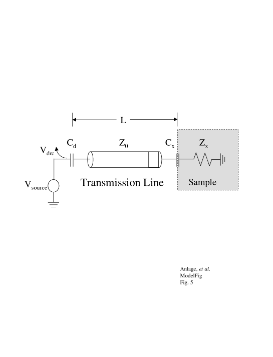
One can calculate the signal measured in the detector Vdrc in terms of the source driving voltage, Vsource. In the simplest case, one finds the following expression for the reflectivity of the resonator:
| (1) |
where Z Z0 is the characteristic impedance of the transmission line, P is the directional coupler voltage fraction, Zd = 1/, is the complex propagation constant of the transmission line of length L, and Zx is the impedance of the capacitor Cx in series with the sample.
The presence of the sample modifies the resonance of the microscope in several ways. First, as the probe-sample distance varies, so does the capacitance Cx. Consider a metallic sample below a blunt probe (e.g., Fig. 3(a)). If the sample is much closer than the probe diameter, there is a parallel-plate capacitance between the probe and the sample. As the sample approaches the probe, this capacitance will increase, and the resonant frequency will decrease. This is because the increased capacitance at the end of the transmission line will effectively lengthen the resonator. Ultimately as the sample comes into contact with the probe, a short-circuit condition is achieved and the microscope becomes a quarter-wave resonator. Hence, the greatest frequency shift expected is that from converting a half-wave to a quarter-wave resonator, which is half the distance between neighboring modes in either the open circuit or short-circuit microscope.
4.3 Frequency Coverage
Because the microscope is a transmission-line resonator with many closely spaced modes, and because each mode can be used for imaging, the microscope is a tremendously broadband instrument. In a typical design, the transmission-line resonator has a length of approximately 1 m, giving a fundamental mode at about 125 MHz, and harmonic modes at integer multiples of this frequency. Hence, imaging can be done up to frequencies where higher-order modes begin to propagate in the coaxial cable, which can be over 100 GHz for small diameter cable. The only other limitation is the microwave electronics required to operate the microscope, such as the source, directional coupler, detector and connectors. However, using modern sources, electronics and the 1-mm standard connector, a 100+ GHz imaging bandwidth can be achieved.
4.4 Temperature range
Our microscopes work well at room temperature. However, we also have constructed a cryogenic version of the microwave microscope. In this case only the probe and part of the resonator is actually held at cryogenic temperatures, along with the sample. Many images have been acquired at liquid-nitrogen temperature (77 K) in both materials and device-imaging modes [51, 74, 76]. We see no reason why this cannot be extended to pumped helium temperatures (1.2 K). At the other extreme, high-temperature coaxial cables exist which can be used for imaging up to 1000∘C [69].
4.5 Other Independent Parameters
One can imagine introducing other quantities into the sample during microwave microscopy. For instance, light illumination is an obvious degree of freedom. We have found that measurements of tunability are very interesting with the scanning near-field microwave microscope. In this case the use of external electric and magnetic fields is most important.
Electric field
We have developed a technique to introduce a local and tunable electric field in our microwave microscope when imaging in contact mode (Fig. 2). A dc electric bias voltage can be applied to the center conductor of the microwave probe through a bias tee. This will create an electric field between the probe tip and the surrounding grounded surfaces. By introducing a suitable ground plane, controlled electric fields can be applied to the sample being imaged at microwave frequencies [48].
Magnetic field
We also can introduce a static magnetic field on samples being imaged by the microwave microscope using an electromagnet. The field can be modulated for imaging magnetic resonant phenomena in the sample.
5 Quantitative Imaging with the Near-Field Microwave Microscope
Here we present some of the results on quantitative imaging with our microscope. Very simply, one expects lossy properties of the sample shown in the model of Fig. 5 to affect the Q of the microscope, while reactive properties and topography will primarily affect the resonant frequency.
5.1 Topography
Images obtained from resonant near-field scanning microwave microscopes are the result of two distinct contrast mechanisms: shifts in the resonant frequency due to electrical coupling between the probe and the sample, and changes in the quality factor Q of the resonator due to losses in the sample [46, 47]. Such images will inevitably contain intrinsic information about a sample (such as dielectric constant or surface resistance) as well as extrinsic information (such as surface topography). To facilitate quantitative imaging of intrinsic material properties, it is essential to be able to accurately account for the effects of finite probe-sample separation and topography.
The interaction between the probe and a metallic sample can be represented by a capacitance Cx between the sample and the inner conductor of the probe, analogous to the mechanism in scanning capacitance microscopy [44, 55]. For a highly conducting sample and a small probe-sample capacitance Cx, i.e., Cx L/cZ0, the reflected voltage Vdrc at the output of the directional coupler can be written as above in Eq. (1) with where c is the speed of light, and is the angular frequency of the source. A plot of Eq. (1) versus frequency would show a series of dips corresponding to enhanced absorption at the resonant frequencies [44]. For Cx=0 and Cd=0, the resonant frequencies are fn=nc/(2L), for n=1,2, …, where is the dielectric constant of the transmission line; for our system a resonance occurs every 125 MHz. For small Cx, the n-th resonant frequency changes by:
.
Since Cx depends on the distance between the inner conductor and the sample, this equation implies that f can be used to determine the topography of the sample. When the sample is very close to the probe, one expects that Cx A/h, so that , where is the area of the center conductor of the probe. On the other hand, when the sample is far from the probe, one must resort to numerical simulation to find Cx(h). To find Cx(h) for the coaxial probe geometry, we solved Poisson’s equation using a finite difference method on a 200 by 150 cell grid. The overall experimental behavior is qualitatively well described by the numerical simulation, including the weak frequency shifts observed at large separation. For convenience, we parameterize our measured calibration curves with an empirical function to easily transform measured frequency shifts to absolute heights.
The topographic imaging capabilities of the system were demonstrated by imaging an uneven, metallic sample: a U.S. quarter-dollar coin. First, the frequency shift was recorded as a function of position over the entire sample. We next measured the frequency shift versus height at a fixed position above a flat part of the sample - see Fig. 2 of reference [55] - and determined the transfer function h(f). Using h(f), we then transformed the frequency-shift image into a topographic surface plot - see Fig. 3(b) of reference [55].
As a result of this work, we can quantitatively account for the contribution of topography to frequency-shift images. Our technique allows for a height resolution of 55 nm for a 30-m probe-sample separation and about 40 m at a separation of 1.75 mm [55]. The technique is simple and should be readily extendible to non-metallic samples, smaller probes and closer or farther separations.
5.2 Sheet resistance
Based on simple reasoning, we expect that the losses of the sample will affect the quality factor Q of the microscope. A simple situation to study is that of a resistive thin-film on a dielectric substrate with a thickness much less than the skin depth. In this case one can show that the sample presents a sheet resistance Rx = /t to the microscope, where is the thin-film resistivity and t is the local thickness of the film. To determine the relationship between Q0 and sample sheet resistance (), we used a variable-thickness aluminum thin-film on a glass substrate [46]. The cross-section of the thin-film is wedge-shaped, implying a spatially-varying sheet resistance. Using a probe with a 500-m-diameter center conductor in non-contact mode, and selecting a resonance of the microscope with a frequency of 7.5 GHz, we acquired frequency-shift and Q0 data. We then cut the sample into narrow strips to take two-point resistance measurements and determine the local sheet resistance. We find that Q0 reaches a maximum as ; as increases, Q0 drops due to loss from currents induced in the sample, reaching a minimum around for a height of 50 m. Similarly, as , Q0 increases due to diminishing currents in the sample. This means that is a double-valued function of Q0. This presents a problem for converting the measured Q0 to . However, is a single-valued function of the frequency shift [46], allowing one to use the frequency-shift data to determine which branch of the Q curve should be used.
To explore the capabilities of our system, we scanned a thin-film of YBa2Cu3O7-δ (YBCO) on a 5-cm-diameter sapphire substrate at room temperature [47]. The film was deposited using pulsed laser deposition with the sample temperature controlled by radiant heating. The sample was rotated about its center during deposition, with the 3-cm-diameter plume held at a position halfway between the center and the edge. The thickness of the YBCO thin-film varied from about 100 nm at the edge to 200 nm near the center.
Figure 6 shows two microwave images of the YBCO sample. The frequency shift [Fig. 6(a)] and Q0 [Fig. 6(b)] were acquired simultaneously, using a probe with a 500-m-diameter center conductor at a height of approximately 50 m above the sample. The scan took approximately 10 minutes to complete, with raster lines 0.5 mm apart. The frequency shifts in Fig. 6(a) are relative to the resonant frequency of 7.5 GHz when the probe was far away (1 mm) from the sample; the resonant frequency shifted downward by more than 2.2 MHz when the probe was above the center of the sample. Noting that the resonant frequency drops monotonically between the edge and the center of the film, and that the resonant frequency is a monotonically increasing function of sheet resistance [46], we conclude that the sheet resistance decreases monotonically between the edge and the center.
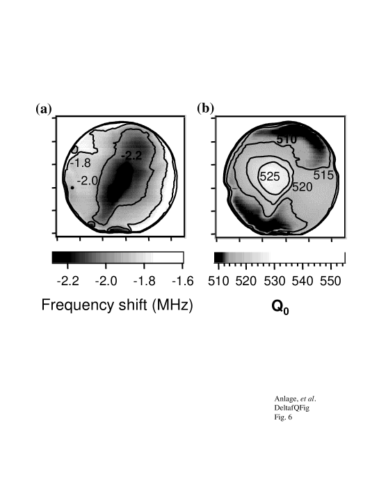
The frequency shift and Q0 images [Fig. 6(a) and (b)] differ slightly in the shape of the contour lines. This is due to the 300-m-thick substrate being warped, causing a variation of a few microns in the probe-sample separation during the scan. In practice, the frequency shift (f) is dominated by topography, but also has contributions from Rx. The change in Q is dominated by sheet resistance, but also has contributions from the topography. To deal with this, we have devised a way to deconvolve these influences and produce images of sheet resistance which are not contaminated by topographic features, and topographic images which are not contaminated by sheet resistance variations. The results are shown in Fig. 7. Figure 7(b) confirms that the film does, indeed, have a lower sheet resistance near the center, as was intended when the film was deposited. We note that the sheet resistance does not have a simple radial dependence, due to either non-stoichiometry or defects in the film. Figure 7(a) shows that the wafer is, indeed, warped, with a higher ridge running from upper right to lower left.
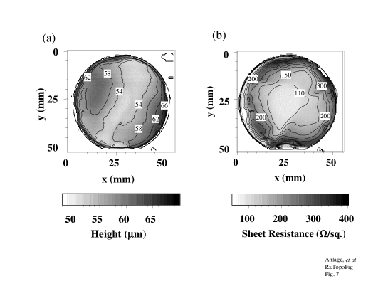
After scanning the YBCO film, we patterned it and made four-point dc resistance measurements throughout the wafer. The dc sheet resistance had a spatial dependence identical to the microwave data in Fig. 7(b) [51]. However, the absolute values were approximately twice as large as the microwave results, most likely due to degradation of the film during patterning. We also found from surface profilometer traces that the topography image of Fig. 7(a) is quantitatively correct.
We have estimated the sheet resistance sensitivity for the microscope as = , for using a probe with a 500-m-diameter center conductor at a height of 50 m and a frequency of 7.5 GHz [47]. The sensitivity scales with the capacitance between the probe center conductor and the sample (); increasing the diameter of the probe center conductor and/or decreasing the probe-sample separation would improve the sensitivity.
5.3 Dielectric Constant
The ability to image variations in relative permittivity or dielectric constant is useful for both fundamental and applied reasons. For example, the dielectric properties of thin-film ferroelectric materials are of interest in studying the finite-size effect on the ferroelectric phase transition. In thin-film microelectronics, testing for variations in dielectric constant can be used for quality control or to develop better growth techniques. Also, knowledge of the dielectric constant at microwave frequencies is of great importance for the design of broadband circuits and future generations of high-speed microprocessors.
Linear dielectric response - Non-Contact Mode
We began our studies of dielectric materials with measurements in non-contact mode with a blunt probe (Fig. 3(a)) [53]. To calibrate the system for dielectric measurements, we constructed a test sample by placing six pieces of different dielectric material into the bottom of a square plastic mold and pouring epoxy into the mold. In addition, silicone adhesive was used to hold down each piece. After the epoxy cured, the test sample was removed from the mold, polished and positioned on the XY table. The materials embedded in the epoxy were silicon, glass microscope slide, SrTiO3, Teflon, sapphire and LaAlO3. All six pieces were approximately 500-m thick and about 6 mm x 8 mm in size. The overall thickness of the test sample was 6 mm.
We measured the frequency shift f versus height h above the six pieces, which have dielectric constants ranging from 2.1 to about 230. We also tested the epoxy which has an unknown dielectric constant. Each piece, as well as the probe, was flat and smooth on the scale of 5 m, as judged by an optical microscope. For these measurements, we used a probe with a 480-m center-conductor diameter and a source frequency of 9.08 GHz. For each scan, the probe was first brought in contact with a dielectric and the frequency shift f was recorded as the height was systematically increased. Samples with the largest dielectric constant produced the largest frequency shift, as expected [53]. The largest shift we observed was 26.2 MHz, when the probe was in contact with a SrTiO3 sample with 230 [53]. The smallest shift we found was -1.2 MHz when the probe was in contact with a Teflon sample with 2.1 [53]. The frequency shift is essentially zero above 1 mm and saturates when the probe-sample distance is smaller than a few microns.
We used the above information to construct an empirical calibration curve that directly relates the frequency shift to the dielectric constant . In order to construct the calibration curve we took the difference between the frequency shift at two different heights, h1 and h2, i.e., fd=f(h2)-f(h1), where h2 is far away (h2 1000 m). By taking the difference, we eliminated the effect of drift in the microwave source frequency. Proceeding this way for the test samples, we constructed two calibration curves of fd versus - see Fig. 2 of reference [53] - one curve for h1=10 m and h2=1.1 mm, and the other for h1=100 m and h2=1.1 mm. We then parameterized each calibration curve with an empirical function, allowing us to easily transform any measured frequency shift to a dielectric constant. From these curves we found that we can enhance the sensitivity to the dielectric constant considerably by using a small probe height. On the other hand, at closer probe-sample separations the influence of topographic features will be enhanced. Hence, it is very important to either control the height of the probe or to de-convolve the topography from the resulting frequency shift and Q images taken in non-contact mode.
Linear dielectric response - Contact Mode
To avoid the issue of topographic features corrupting the dielectric imaging, we have developed a contact-mode version of dielectric imaging [48]. We use the near-field scanning microwave microscope with a sharp protruding center conductor. The probe tip, which has a radius of curvature m - see inset to Fig. 2 and Fig. 3(b) - is held fixed, while the sample is supported by a spring-loaded cantilever applying a controlled normal force of about 50 N between the probe tip and the sample [48]. Due to the concentration of the microwave fields at the tip, the boundary condition of the resonator, and hence, the resonant frequency and quality factor Q are perturbed depending on the dielectric properties of the region of the sample immediately beneath the probe tip. We have shown that the spatial resolution of the microscope in this mode of operation is about 1 m [45].
To observe the microscope’s response to sample dielectric permittivity , we monitored the frequency-shift signal while scanning samples with known . With well-characterized 500-m-thick bulk dielectrics, we observed that the microscope frequency shift monotonically increases in the negative direction with increasing sample permittivity, as noted above [53]. We observed similar behavior with thin-film dielectric samples.
For comparison, we did a finite-element calculation of the rf electric field near the probe tip. Because the probe-tip radius is much less than the wavelength cm at 7 GHz), a static calculation of the electric field is sufficient [65]. Cylindrical symmetry further simplifies the problem to two dimensions. We represent the probe tip as a cone with a blunt end, held at a potential of V. Using relaxation methods we solved Poisson’s equation for the potential, , on a rectangular grid representing the region around the probe tip. The two variables we used to represent the properties of the probe were the aspect ratio of the probe tip () and the radius of the blunt end.
Since the sample represents a small perturbation to the resonator, we can use perturbation theory [48] to find the change in the resonant frequency:
| (2) |
where 1 and 2, and and are the unperturbed and perturbed electric fields, and relative permittivities of two samples, respectively; is the energy stored in the resonator, and the integral is over the volume of the sample. We compute an approximate using the fact that the loaded quality factor [47] of the resonator is , where is the resonant frequency, and is the power loss in the resonator. Using four bulk samples with known relative dielectric permittivities between 2.1 and 305, and fixing m, we used as a fitting parameter to obtain agreement between the model results from Eq. (2) and our data at 7.2 GHz; we found agreement to within 10 % for several different probe tips, with .
To extend this calibration model to thin films, we extend the finite-element calculation to include a thin-film on top of the dielectric sample substrate. Once a probe’s parameter is determined using the bulk calibration described above, we use the thin-film model combined with Eq. (2), integrating over the volume of the thin-film, to obtain a functional relationship between and the dielectric permittivity of the thin-film. Using the thin-film model, we found that for high-permittivity () thin films, the microwave microscope is primarily sensitive to the in-plane component of the permittivity tensor.
Figure 8(a) shows a quantitative permittivity image of a sample consisting of a 440-nm SrTiO3 (STO) thin-film on a 500-m LaAlO3 (LAO) substrate. The film was made by pulsed laser deposition at 700∘ C, in 200 mTorr of O2. The film is paraelectric at room temperature. In the microwave (7.2 GHz) permittivity image [Fig. 8(a)], the film shows a dielectric constant on the order of 180 over most of its area (20 m by 20 m here). Several low-permittivity defects on the film also are visible. From atomic force microscopy measurements we find that these features are second-phase laser particles deposited on top of the STO film. Their greater thickness is part of the reason the relative permittivity is lower in the image.
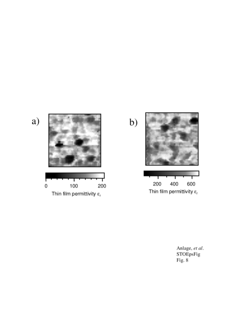
Figure 8(b) shows a quantitative permittivity image of a sample consisting of a 275-nm Ba0.60Sr0.40TiO3 (BST) thin-film on a 500-m LAO substrate. The film also was made by pulsed laser deposition at 700∘ C, in 200 mTorr of O2. The film is paraelectric at room temperature. It shows a larger average dielectric constant than STO, but also contains laser particles. The fine structure in Figs. 8 may be indicative of varying dielectric properties from grain to grain in the films.
Nonlinear dielectric response in contact mode
In order to measure the local dielectric tunability of thin films, we apply a dc electric field to the sample by voltage biasing () the probe tip - see Fig. 2. A grounded metallic counterelectrode layer immediately beneath the dielectric thin-film acts as a ground plane. To prevent the counterelectrode from dominating the microwave measurement, thus minimizing its effect on the microwave fields - we ignored the counterelectrode in our static field model - the sheet resistance of the counterelectrode should be as high as possible. In our case, we use low carrier density La0.95Sr0.05CoO3 with a thickness of 100 nm, giving a sheet resistance . We have confirmed by experiment and model calculation [46, 48] that the contribution of the counterelectrode to the frequency shift is small ( kHz) relative to the contribution from a dielectric thin-film with thickness 100 nm ( kHz).
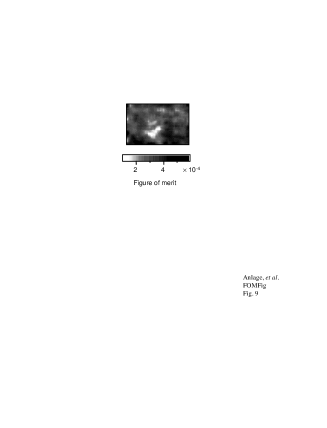
We can examine the tunability of the dielectric properties at a fixed point on the sample and generate a hysteresis loop [48, 64]. As expected, the permittivity goes down and the Q goes up when a voltage is applied. To image the tunability of the sample, we change the bias voltage applied to the probe tip and image the dielectric constant again. A tunability figure of merit can be defined with this data. In general, one wants a highly tunable material which is not very lossy. Hence, the figure of merit to maximize is K = (/)/tan, where is the change in dielectric constant upon tuning with some fixed electric field, and tan is the dielectric loss at zero bias. In our case we can define a similar figure of merit with the raw data as K = (/), where is the frequency shift due to tuning a 400-nm-thick Ba0.60Sr0.40TiO3 (BST) thin-film with a bias of 2.5 V, and Q is the unbiased quality factor of the microscope. Figure 9 shows the resulting figure of merit image over a 20-m by 13-m area. The main region of very low tunability (white area) is most likely a laser-deposited particle of non-paraelectric material. However, there are smaller regions of low tunability which are separated by just a few microns from regions of very good tunability. This demonstrates the power of the scanning microwave microscope to delve into the microstructure-property relationship on the microscopic scale.
The microwave technique we use is sensitive to both film thickness and permittivity. As a result, the permittivity of the large defects in Fig. 8(a) is underestimated due to the change in film thickness at these locations, which we have confirmed with our model. However, by examining an AFM image, topographic features can be readily distinguished from permittivity features. We have further shown that in most of the images the topography is too small to account for a significant contribution to the observed permittivity contrast. We can calculate the sensitivity of the microwave microscope by observing the noise in the dielectric permittivity and tunability data. For a 370-nm-thick film on a 500-m-thick LAO substrate, with an averaging time of 40 ms, we find that the relative dielectric permittivity sensitivity is at , and the tunability sensitivity is V-1 [48, 64]
6 Future Prospects
Having demonstrated quantitative imaging of losses, topography and dielectric constant on the micron length scale and below, what is next for this impressive instrument? Ongoing research is focused on a number of issues. The first is an effort to improve the spatial resolution of the microscope while maintaining its quantitative capabilities. The frontier seems to be improved field-enhancement techniques, similar to those now being pursued in near-field scanning optical microscopy. The exploitation of resonant electromagnetic phenomena combined with cantilever techniques is another tool for improving spatial resolution. Another important issue is the utilization of the microwave microscope’s broad frequency bandwidth. This can be used to examine frequency-dependent phenomena, such as electronic and magnetic dynamics in correlated electron systems.
Superconducting materials present an interesting problem for near-field microwave microscopes. Already progress has been made in imaging the transition temperature in superconducting thin films [43, 70, 71, 72]. Although a superconducting microscope is probably required to image surface impedance on the micron scale, it may be possible to learn more from conventional microscopes which study nonlinearities [52, 54, 73]. Our group also has imaged electric fields in the near-field of operating superconducting microwave devices at 77 K and above [73, 74, 75, 76]. The effort is focused on isolating the local sources of nonlinearity under operating conditions.
Many other possibilities of electrodynamics experiments remain to be exploited. What is clear is that a new era of local electromagnetic experiments has begun.
7 Conclusions
We have given a short introduction to the new field of near-field microwave electrodynamics measurements. Five major developments of near-field microwave microscopy have been identified. We have presented a thorough introduction to the form of microscopy we have developed at the University of Maryland. Quantitative images of metallic sheet resistance, topography, dielectric constant and dielectric tunability have been presented. Great potential exists for new quantitative electrodynamics measurements on ever finer length scales.
7.1 Acknowledgements
This work could not have been possible without the assistance of S. K. Dutta, B. J. Feenstra, W. Hu, A. Schwartz, J. Lee and A. Thanawalla. This work has been supported by the Maryland/NSF Materials Research Science and Engineering Center on Oxide Thin Films DMR 9632521, as well as NSF grant # ECS-9632811, an NSF SBIR (DMI-9710717) subcontract from Neocera, Inc. and by the Maryland Center for Superconductivity Research.
References
- [1] A. B. Pippard, “The surface impedance of superconductors and normal metals at high frequencies: I. Resistance of superconducting tin and mercury at 1200 Mcyc./sec.,” Proc. Roy. Soc. A 191, 370-384 (1947).
- [2] J. C. Slater, “Microwave Electronics,” Rev. Mod. Phys. 18, 441-521 (1946); L. C. Maier, Jr. and J. C. Slater, “Field Strength Measurements in Resonant Cavities,” J. Appl. Phys. 23, 68-83 (1952).
- [3] O. Klein, S. Donovan, M. Dressel, and G. Grüner, “Microwave Cavity Perturbation Technique: Part I: Principles,” Int. J. Infrared and Millimeter Waves 14, 2423- 2457 (1993); S. Donovan, O. Klein, M. Dressel, K. Holczer, and G. Grüner, “Microwave Cavity Perturbation Technique: Part II: Experimental Scheme,” Int. J. Infrared and Millimeter Waves 14, 2459-2487 (1993); M. Dressel, O. Klein, S. Donovan, and G. Grüner, “Microwave Cavity Perturbation Technique: Part III: Applications,” Int. J. Infrared and Millimeter Waves 14, 2489-2517 (1993).
- [4] H. Ning, H. Duan, P. D. Kirven, A. M. Hermann, and T. Datta, “Magnetic Penetration Depth in High-Tc Superconducting Tl2Ca1Ba2Cu2O8-δ Single Crystals,” J. Super. 5, 503-509 (1992).
- [5] C. E. Gough, and N. J. Exon, “Microwave response of anisotropic high-temperature- superconductor crystals,” Phys. Rev. B 50, 488-495 (1994).
- [6] R. C. Taber, “A parallel plate resonator technique for microwave loss measurements on superconductors,” Rev. Sci. Instrum. 61, 2200-2206 (1990).
- [7] V. V. Talanov, L. V. Mercaldo, S. M. Anlage and J. H. Claassen, “Measurement of the absolute penetration depth and surface resistance of superconductors and normal metals with the variable spacing parallel plate resonator,” to be published in Rev. Sci. Instrum. (2000).
- [8] John Gallop, L. Hao, F. Abbas, “Spatially Resolved Measurements of HTS Microwave Surface Impedance,” Physica C 282-287, 1579-1580 (1997); L. Hao, J. C. Gallop, “Spatially Resolved Measurements of HTS Microwave Surface Impedance,” IEEE Trans. Appl. Supercond. 9, 1944-1947 (1999).
- [9] C. Wilker, Z-Y. Shen, V. X. Nguyen, and M. S. Brenner, “A sapphire resonator for microwave characterization of superconducting thin films,” IEEE Trans. Appl. Supercond. 3, 1457-1460 (1993).
- [10] Steve Hogan, Sigurd Wagner, and Frank S. Barnes, “Resistivity measurement of thin semiconductor films on metallic substrates,” Appl. Phys. Lett. 35, 77-79 (1979).
- [11] J. S. Martens, V. M. Hietala, D. S. Ginley, T. E. Zipperian, and G. K. G. Hohenwarter, “Confocal resonators for measuring the surface resistance of high- temperature superconducting films,” Appl. Phys. Lett. 58, 2543-2545 (1991).
- [12] E. Keskin, K. Numssen, and J. Halbritter, “Defects in YBCO relevant for rf superconductivity: T-, f- and H-dependencies,” IEEE Trans. Appl. Supercon. 9, 2452 (1999).
- [13] E. F. Skelton, A. R. Drews, M. S. Osofsky, S. B. Qadri, J. Z. Hu, T. A. Vanderah, J. L. Peng, and R. L. Greene, “Direct observation of Microscopic inhomogeneities with energy-dispersive diffraction of synchrotron-produced x-rays,” Science 263, 1416-1418 (1994).
- [14] A. F. Hebard, A. T. Fiory, M. P. Siegal, J. M. Phillips, and R. C. Haddon, “Vortex- pair nucleation at defects: A mechanism for anoalous temperature dependence in the superconducting screening length,” Phys. Rev. B 44, 9753-9756 (1991).
- [15] G. Hampel, B. Batlogg, K. Krishana, N. P. Ong, W. Prusseit, H. Kinder, A. C. Anderson, “Third-order nonlinear microwave response of YBa2Cu3O7-δ thin films and single crystals,” Appl. Phys. Lett. 71, 3904-3906 (1997).
- [16] C. P. Bidinosti, W. N. Hardy, D. A. Bonn, and R. Liang, “Measurements of the Magnetic Field Dependence of l in YBa2Cu3O6.95: Results as a Function of Temperature and Field Orientation,” Phys. Rev. Lett. 83, 3277-3280 (1999).
- [17] A. Carrington, R. W. Giannetta, J. T. Kim, and J. Giapintzakis, “Absence of non- linear Meissner effect in YBa2Cu3O6.95,” Phys. Rev. B 59, R14173-14176 (1999).
- [18] E. A. Synge, “A suggested method for extending microscopic resolution into the ultra-microscopic region,” Phil. Mag. C 6, 356-362 (1928).
- [19] Zdenek Frait, “The use of high frequency modulation in studying ferromagnetic resonance,” Czeck. J. Phys. 9, 403-404 (1959); Z. Frait, V. Kambersky, Z. Malek, and M. Ondris, “Local variations of uniaxial anisotropy in thin films,” Czeck. J. Phys. B10, 616-617 (1960).
- [20] R. F. Soohoo, “A Microwave Magnetic Microscope,” J. Appl. Phys. 33, 1276-1277 (1962).
- [21] S. E. Lofland, S. M. Bhagat, H. L. Ju, G. C. Xiong, T. Venkatesan, and R. L. Greene, “Ferromagnetic resonance and magnetic homogeneity in a giant-magnetoresistance material La2/3Ba1/3MnO3,” Phys. Rev. B 52, 15058-15061 (1995).
- [22] M. Ikeya and T. Miki, “ESR Microscopic Imaging with Microfabricated Field Gradient Coils,” Jap. J. Appl. Phys. 26, L929-L931 (1987); M. Ikeya, M. Furusawa, and M. Kasuyai, “Near-field scanning electron spin resonance microscopy,” Scanning Microscopy 4, 245-248 (1990).
- [23] E. A. Ash and G. Nicholls, “Super-resolution Aperture Scanning Microscope,” Nature 237, 510-512 (1972).
- [24] D. W. Pohl, W. Denk, and M. Lanz, “Optical stethoscopy: Image recording with resolution /20,” Appl. Phys. Lett. 44, 651-653 (1984).
- [25] E. Betzig, M. Isaacson and A. Lewis, “Collection mode near-field scanning optical microscopy,” Appl. Phys. Lett. 51, 2088-2090 (1987).
- [26] C. A. Bryant and J. B. Gunn, “Noncontact Technique of the Local Measurement of Semiconductor Resistivity,” Rev. Sci. Instrum. 36, 1614-1617 (1965).
- [27] Y. S. Xu and R. G. Bosisio, “Nondestructive Measurements of the Resistivity of Thin Conductive Films and the Dielectric Constant of Thin Substrates Using an Open-Ended Coaxila Line,” IEE Proc. H 139, 500-506 (1992).
- [28] M. A. Stuchly and S. S. Stuchly, “Coaxial Line Reflection Methods for Measuring Dielectric Properties of Biological Substances at Radio and Microwave Frequencies - A Review,” IEEE Trans. Instrum. and Meas. IM-29, 176-183 (1980); M. A. Stuchly, M. M. Brady, S. S. Stuchly and G. Gajda, “Equivalent Circuit of an Open-Ended Coaxial Line in a Lossy Dielectric,” IEEE Trans. Instrum. and Meas. IM-31, 116-119 (1982); T. W. Athey, M. A. Stuchly and S. S. Stuchly, “Measurement of Radio Frequency Permittivity of Biological Tissues with an Open-Ended Coaxial Line: Part I,” IEEE Trans. Microwave Theory and Tech. MTT-30, 82-86 (1982); M. A. Stuchly, T. W. Athey, G. M. Samaras and G. E. Taylor, “Measurement of Radio Frequency Permittivity of Biological Tissues with an Open-Ended Coaxial Line: Part II - Experimental Results,” IEEE Trans. Microwave Theory and Tech. MTT-30, 87-92 (1982); G. B. Gajda and S. S. Stuchly, “Numerical Analysis of Open-Ended Coaxial Lines,” IEEE Trans. Microwave Theory and Tech. MTT-31, 380-384 (1983).
- [29] E. C. Burdette, F. L. Cain, and J. Seals, “In Vivo Probe Measurement Technique for Determining Dielectric Properties at VHF Through Microwave Frequencies,” IEEE Trans. Microwave Theory Tech. MTT-28, 414-427 (1980).
- [30] M. Fee, S. Chu and T. W. Hänsch, “Scanning electromagnetic transmission line microscope with sub-wavelength resolution,” Optics Communications 69, 219-224 (1989).
- [31] S. J. Stranick and P. S. Weiss, “A versatile microwave-frequency-compatible scanning tunneling microscope,” Rev. Sci. Instrum. 64, 1232-1234 (1993); S. J. Stranick and P. S. Weiss, “A tunable microwave frequency alternating current scanning tunneling microscope,” Rev. Sci. Instrum. 65, 918-921 (1994); L. A. Bumm and P. S. Weiss, “Small cavity nonresonant tunable microwave-frequency alternating current scanning tunneling microscope,” Rev. Sci. Instrum. 66, 4140-4145 (1995).
- [32] G. Q. Jiang, W. H. Wong, E. Y. Raskovich, W. G. Clark, W. A. Hines, J. Sanny, “Open- ended coaxial-line technique for the measurement of the microwave dielectric constant for low-loss solids and liquids,” Rev. Sci. Instrum. 64, 1614-1621 (1993).
- [33] K. Asami, “The scanning dielectric microscope,” Meas. Sci. Technol. 5, 589-592 (1994).
- [34] R. J. Gutman and J. M. Borrego, “Microwave scanning microscopy for planar structure diagnostics,” IEEE MTT Digest, 281-284 (1987); Bhimnathwala and J. M. Borrego, “Measurement of the sheet resistance of doped layers in semiconductors by microwave reflection,” J. Vac. Sci. Technol. B 12 , 395-398 (1994).
- [35] N. Qaddoumi and R. Zoughi, “Preliminary study of the influences of effective dielectric constant and nonuniform probe apeture field distribution on near field microwave images,” Materials Evaluation, Oct., 1169-1173 (1997).
- [36] M. Golosovsky and D. Davidov, “Novel millimeter-wave near-field resistivity microscope,” Appl. Phys. Lett. 68, 1579-1581 (1996); M. Golosovsky, A. Galkin, and D. Davidov, “High-Spatial Resolution Resistivity Mapping of Large-Area YBCO Films by a Near-Field Millimeter-Wave Microscope,” IEEE MTT 44, 1390-1392 (1996); M. Golosovsky, A. Lann, and D. Davidov, “A millimeter-wave near-field scanning probe with an optical distance control,” Ultramicroscopy 71, 133-141 (1998); A. F. Lann, M. Golosovsky, D. Davidov, and A. Frenkel, “Combined millimeter-wave near-field microscope and capacitance distance control for the quantitative mapping of sheet resistance of conducting layers,” Appl. Phys. Lett. 73, 2832-2834 (1998); A. F. Lann, M. Golosovsky, D. Davidov, and A. Frenkel, “Microwave near-field polarimetry,” Appl. Phys. Lett. 75, 603-605 (1999).
- [37] J. Bae, T. Okamoto, T. Fujii, K. Mizuno, T. Nozokido, ”Experimental demonstration for scanning near-field optical microscopy using a metal micro-slit probe at millimeter wavelengths,” Appl. Phys. Lett. 71, 3581-3583 (1997).
- [38] M. Tabib-Azar, N. Shoemaker and S. Harris, “Non-destructive characterization of materials by evanescent microwaves,” Meas. Sci. Tech., 4, 583-590 (1993); M. Tabib-Azar, D. -P. Su, A. Pohar, S. R. LeClair, and G. Ponchak, “0.4 m spatial resolution with 1 GHz ( = 30 cm) evanescent microwave probe,” Rev. Sci. Instrum., 70, 1725-1729 (1999); M. Tabib-Azar, P. S. Pathak, G. Ponchak, and S. LeClair, “Nondestructive superresolution imaging of defects and nonuniformities in metals, semiconductors, dielectrics, composites, and plants using evanescent microwaves,” Rev. Sci. Instrum., 70, 2783-2792 (1999); M. Tabib-Azar, R. Ciocan, G. Ponchak, and S. R. LeClair, “Transient thermography using evanescent microwave microscope,” Rev. Sci. Instrum., 70, 3387-3390 (1999); G. Ponchak, D. Akinwande, R. Ciocan, S. R. LeClair and M. Tabib-Azar, “Evanescent Microwave Probes Using Coplanar Waveguide and Stripline for Super-Resolution Imaging of Materials,” IEEE MTT-S Digest, (1999).
- [39] F. Keilmann, US Patent 4,994,818, filed Oct. 27, 1989; R. Merz, F. Keilmann, R. J. Haug, and K. Ploog, “Nonequilibrium Edge-State Transport Resolved by Far-Infrared Microscopy,” Phys. Rev. Lett. 70, 651-653 (1993); F. Keilmann, “FIR Microscopy,” Infrared Phys. Technol. 36, 217-224 (1995); F. Keilmann, D. W. van der Weide, T. Eickelkamp, R. Merz, and D. Stöckle, “Extreme sub-wavlength resolution with a scanning radio-frequency transmission microscope,” Optics Commun. 129, 15-18 (1996); B. Knoll, F. Keilmann, A. Kramer, and R. Guckenberger, “Contrast of microwave near-field microscopy,” Appl. Phys. Lett. 70, 2667-2669 (1997).
- [40] R. G. Bosisio, M. Giroux, and D. Couderc, “Paper Sheet Moisture Measurements by Microwave Phase Perturbation Techniques,” J. Microwave Power 5, 25-34 (1970).
- [41] E. Tanabe and W. T. Joines, “A Nondestructive Method for Measuring the Complex Permittivity of Dielectric Materials at Microwave Frequencies Using an Open Transmission Line Resonator,” IEEE Trans. Instrum. and Meas. IM-25, 222-226 (1976).
- [42] Y. Cho, A. Kirihara and T. Saeki, “Scanning nonlinear dielectric microscope,” Rev. Sci. Instrum. 67, 2297-2303 (1996); Y. Cho, S. Kazuta, and K. Matsuura, “Scanning nonlinear dielectric microscopy with nanometer resolution,” Appl. Phys. Lett. 75, 2833-2835 (1999).
- [43] T. Wei, X.-D. Xiang, W. G. Wallace-Freedman and P. G. Schultz, “Scanning tip microwave near-field microscope,” Appl. Phys. Lett. 68, 3506-3508 (1996); Y. Lu, T. Wei, F. Duewer, Y. Lu, N. Ming, P. G. Schultz and X.-D. Xiang, “Nondestructive Imaging of Dielectric-Constant Profiles and Ferroelectric Domains with a Scanning-Tip Microwave Near-Field Microscope,” Science 276, 2004-2006 (1997); C. Gao, T. Wei, F. Duewer, Y. Lu and X.-D. Xiang, “High spatial resolution quantitative microwave impedance microscopy by a scanning tip microwave near-field microscope,” Appl. Phys. Lett. 71, 1872-1874 (1997); I. Takeuchi, T. Wei, F. Duewer, Y. K. Yoo, X.-D. Xiang, V. Talyansky, S. P. Pai, G. J. Chen, and T. Venkatesan, “Low temperature scanning-tip microwave near-field microscopy of YBCO films,” Appl. Phys. Lett. 71, 2026-2028 (1997); H. Chang, C. Gao, I. Takeuchi, Y. Yoo, J. Wang, P. G. Schultz, X.-D. Xiang, R. P. Sharma, M. Downes, and T. Venkatesan, “Combinatorial synthesis and high throughput evaluation of ferroelectric/dielectric thin-film libraries for microwave applications,” Appl. Phys. Lett. 72, 2185-2187 (1998); C. Gao, and X.-D. Xiang, “Quantitative microwave near-field microscopy of dielectric properties,” Rev. Sci. Instrum. 69, 3846-3851 (1998).
- [44] C. P. Vlahacos, R. C. Black, S. M. Anlage and F. C. Wellstood, “Near-field Scanning Microwave Microscope with 100 m Resolution,” Appl. Phys. Lett. 69, 3272-3274 (1996).
- [45] Steven M. Anlage, C. P. Vlahacos, Sudeep Dutta, and F. C. Wellstood, “Scanning Microwave Microscopy of Active Superconducting Microwave Devices,” IEEE Trans. Appl. Supercond. 7, 3686-3689 (1997).
- [46] D. E. Steinhauer, C. P. Vlahacos, Sudeep Dutta, F. C. Wellstood, and Steven M. Anlage, “Surface Resistance Imaging with a Scanning Near-Field Microwave Microscope,” Appl. Phys. Lett. 71, 1736-1738 (1997). cond-mat/9712142.
- [47] D. E. Steinhauer, C. P. Vlahacos, S. K. Dutta, B. J. Feenstra, F. C. Wellstood, and Steven M. Anlage, “Quantitative Imaging of Sheet Resistance with a Scanning Near-Field Microwave Microscope,” Appl. Phys. Lett. 72, 861-863 (1998). cond-mat/9712171.
- [48] D. E. Steinhauer, C. P. Vlahacos, C. Canedy, A. Stanishevski, J. Melngailis, R. Ramesh, F. C. Wellstood, and S. M. Anlage, “Imaging of Microwave Permittivity, Tunability, and Damage Recovery in (Ba,Sr)TiO3 Thin Films,” Appl. Phys. Lett. 75, 3180-3182 (1999).
- [49] B. J. Feenstra, C. P. Vlahacos, Ashfaq S. Thanawalla, D. E. Steinhauer, S. K. Dutta, F. C. Wellstood and Steven M. Anlage, “Near-Field Scanning Microwave Microscopy: Measuring Local Microwave Properties and Electric Field Distributions,” IEEE MTT-S Int. Microwave Symp. Digest, p. 965-966 (1998). cond-mat/9802293.
- [50] Steven M. Anlage, C. P. Vlahacos, D. E. Steinhauer, S. K. Dutta, B. J. Feenstra, A. Thanawalla, and F. C. Wellstood, “Low Power Superconducting Microwave Applications and Microwave Microscopy,” Particle Accelerators 61, [321-336]/57-72 (1998). cond-mat/9808195
- [51] Steven M. Anlage, D. E. Steinhauer, C. P. Vlahacos, B. J. Feenstra, A. S. Thanawalla, Wensheng Hu, Sudeep K. Dutta, and F. C. Wellstood, “Superconducting Material Diagnostics using a Scanning Near-Field Microwave Microscope,” IEEE Trans. Appl. Supercond. 9, 4127-4132 (1999). cond-mat/9811158.
- [52] Steven M. Anlage, Wensheng Hu, C. P. Vlahacos, David Steinhauer, B. J. Feenstra, Sudeep K. Dutta, Ashfaq Thanawalla, and F. C. Wellstood, “Microwave Nonlinearities in High-Tc Superconductors: The Truth Is Out There,” J. Supercond. 12, 353-362 (1999). cond-mat/9808194.
- [53] C. P. Vlahacos, D. E. Steinhauer, S. K. Dutta, B. J. Feenstra, Steven M. Anlage, and F. C. Wellstood, “Non-Contact Imaging of Dielectric Constant with a Near-Field Scanning Microwave Microscope,” The Americas Microscopy and Analysis, January, 5-7, (2000).
- [54] Steven M. Anlage, A. S. Thanawalla, A. P. Zhuravel’, W. Hu, C. P. Vlahacos, D. E. Steinhauer, S. K. Dutta, and F. C. Wellstood, “Near-Field Scanning Microwave Microscopy of Superconducting Materials and Devices,” in Advances in Superconductivity XI, ed. by N. Koshizuka and S. Tajima, (Springer-Verlag, Tokyo, 1999), pp. 1079 - 1084.
- [55] C. P. Vlahacos, D. E. Steinhauer, S. K. Dutta, B. J. Feenstra, Steven M. Anlage, and F. C. Wellstood, “Quantitative Topographic Imaging Using a Near-Field Scanning Microwave Microscope,” Appl. Phys. Lett., 72, 1778-1780 (1998). cond-mat/9802139.
- [56] M. J. Werner and R. J. King, “Mapping the of conducting solid films in situ,” MRS Proc. (1996); U.S. Patent #5,334,941, “Microwave reflection resonator sensors,” issued August 2, 1994 to R. J. King.
- [57] Y. Manassen, “Scanning Probe Microscopy and Magnetic Resonance,” Adv. Mater. 6, 401- 404 (1994).
- [58] Z. Zhang, P. C. Hammel and P. Wigen, “Observation of ferromagnetic resonance in a microscopic sample using magnetic resonance force microscopy,” Appl. Phys. Lett. 68, 2005-2007 (1996); Z. Zhang, P. C. Hammel, M. Midzor, M. L. Roukes, and J. R. Childress, “Ferromagnetic resonance force microscopy on microscopic cobalt single layer films,” Appl. Phys. Lett. 73, 2036-2038 (1998).
- [59] K. Wago, D. Botkin, C. S. Yannoni, and D. Rugar, “Paramagnetic and ferromagnetic resonance imaging with a tip-on-cantilever magnetic resonance force microscope,” Appl. Phys. Lett. 72, 2757-2759 (1998).
- [60] B. Knoll, and F. Keilmann, “Near-field probing of vibrational absorption for chemical microscopy,” Nature 399, 134-137 (1999).
- [61] R. C. Black, F. C. Wellstood, E. Dantsker, A. H. Miklich, D. T. Nemeth, D. Koelle, F. Ludwig, and J. Clarke, “Microwave microscopy using a superconducting quantum interference device,” Appl. Phys. Lett. 66, 99-101 (1995); R. C. Black, F. C. Wellstood, E. Dantsker, A. H. Miklich, D. Koelle, F. Ludwig, and J. Clarke, “High-frequency magnetic microscopy using a high-Tc SQUID,” IEEE Trans. Appl. Supercon. 5, 2137-2141 (1995).
- [62] J. E. Aitken, “Swept Frequency Microwave Q-Factor Measurement,” Proc. IEE 123, 855-862 (1976).
- [63] K. Zaki and G. J. Chen, private communication.
- [64] D. E. Steinhauer, C. P. Vlahacos, C. Canedy, A. Stanishevski, J. Melngailis, R. Ramesh, F. C. Wellstood, and S. M. Anlage, “Quantitative Imaging of Permittivity and Tunability with a Near-Field Scanning Microwave Microscope,” submitted to Rev. Sci. Instrum. (1999).
- [65] S. Ramo, J. R. Whinnery and T. van Duzer, Fields and Waves in Communication Electronics, second edition, (Wiley, New York, 1984), p. 445.
- [66] Ichiro Takeuchi, personal communication.
- [67] J. C. Booth, Ph.D. Thesis, “Novel Measurements of the Frequency Dependent Microwave Surface Impedance of Cuprate Thin Film Superconductors,” University of Maryland, 1996.
- [68] G. L. James, “Analysis and Design of TE11-to-HE11 Corrugated Cylindrical Waveguide Mode Converters,” IEEE Trans. Microwave Theory Tech. 29, 1059-1066 (1981).
- [69] D. Gershon, J. P. Calame, Y. Carmel, T. M. Antonsen Jr., and R. M. Hutchen, “Open-ended coaxial probe for high-temperature and broad-band dielectric measurements,” IEEE Trans. Microwave Theory Tech. 47, 1640-1648 (1999).
- [70] B. J. Feenstra, Ashfaq S. Thanawalla, Wensheng Hu, D. E. Steinhauer, Steven M. Anlage, F. C. Wellstood, “Local measurements of normal and superconducting state properties of high Tc superconductors at microwave frequencies,” Bull. Am. Phys. Soc. 44, 1479 (1999).
- [71] A. F. Lann, M. Abu-Teir, M. Golosovsky, D. Davidov, A. Goldgirsch, and V. Berlin, “Magnetic-field-modulated microwave reflectivity of high-Tc superconductors studied by near-field mm-wave microscopy,” Appl. Phys. Lett. 75, 1766-1768 (1999).
- [72] A. F. Lann, M. Abu-Teir, M. Golosovsky, D. Davidov, S. Djordjevic, N. Bontemps, and L. F. Cohen, “A cryogenic microwave scanning near-field probe: Application to study of high-Tc superconductors,” Rev. Sci. Instrum. 70, 4348-4355 (1999).
- [73] Wensheng Hu, B. J. Feenstra, A. S. Thanawalla, F. C. Wellstood, and Steven M. Anlage, “Imaging of Microwave Intermodulation Fields in a Superconducting Microstrip Resonator,” Appl. Phys. Lett. 75, 2824-2826 (1999).
- [74] Ashfaq S. Thanawalla, S. K. Dutta, C. P. Vlahacos, D. E. Steinhauer, B. J. Feenstra, Steven M. Anlage, and F. C. Wellstood, “Microwave Near-Field Imaging of Electric Fields in a Superconducting Microstrip Resonator,” Appl. Phys. Lett. 73, 2491-2493 (1998). cond-mat/9805239.
- [75] S. K. Dutta, C. P. Vlahacos, D. E. Steinhauer, Ashfaq S. Thanawalla, B. J. Feenstra, F. C. Wellstood, Steven M. Anlage, and Harvey S. Newman, “Imaging Microwave Electric Fields Using a Near-Field Scanning Microwave Microscope,” Appl. Phys. Lett. 74, 156-158 (1999). cond-mat/9811140.
- [76] Ashfaq S. Thanawalla, W. Hu, D. E. Steinhauer, S. K. Dutta, B. J. Feenstra, Steven M. Anlage, F. C. Wellstood, and Robert B. Hammond, “Frequency Following Imaging of the Electric Field around Resonant Superconducting Devices using a Near-Field Scanning Microwave Microscope,” IEEE Trans. Appl. Supercond. 9, 3042-3045 (1999). cond-mat/9811141.